國 立 交 通 大 學
顯示科技研究所
碩士論文
以全數位資料驅動操作之
液晶顯示器畫素電路
Liquid Crystal Display Pixel Circuit
Operated by Full-Digital Data Driving
研 究 生:林俊佑 Student : Chun-Yu Lin
指導教授:戴亞翔 博士 Advisor : Dr. Ya-Hsiang Tai
以全數位資料驅動操作之
液晶顯示器畫素電路
Liquid Crystal Display Pixel Circuit
Operated by Full-Digital Data Driving
研 究 生:林俊佑 Student : Chun-Yu Lin
指導教授:戴亞翔 博士 Advisor : Dr. Ya-Hsiang Tai
國立交通大學
顯示科技研究所
碩 士 論 文
A Thesis
Submitted to the Institute of Display
College of Electrical and Computer Engineering
National Chiao Tung University
in Partial Fulfillment of the Requirements
for the Degree of Master
in
Institute of Display
June 2014
Hsinchu, Taiwan, Republic of China
I
以全數位資料驅動操作之
液晶顯示器畫素電路
學生:林俊佑 指導教授:戴亞翔 博士
國立交通大學顯示科技研究所
摘 要
對於液晶顯示器內部所有的零組件來說,資料驅動器的耗能僅次
於背光源,而且其大部分是消耗在訊號轉換上。我們在本篇論文裡提
出一種新式的畫素電路,能夠以全數位訊號來驅動。如此一來,資料
驅動器中的訊號轉換元件將可以被移除,同時大幅度降低元件的功耗。
在提出的畫素電路中包含兩個薄膜電晶體以及一個電阻,以串接的方
式形成畫素電壓的放電路徑。另外有第三顆薄膜電晶體負責將畫素電
容預先充電至指定電壓,當特定畫素電路被掃描訊號開啟後,即可藉
由控制資料訊號的脈寬來完成灰階的設定。我們利用模擬的方式將新
式畫素電路操作在小尺寸與大尺寸面板中,以驗證其運作能力。此外,
還將新式畫素電路與傳統 1T1C 畫素電路互相做比較,項目包含動態
功率消耗、誤差容忍度以及開口率。由結果證實我們提出的畫素電路
在新式驅動方式下,可以有效地降低資料驅動器的能量消耗。
II
Liquid Crystal Display Pixel Circuit
Operated by Full-Digital Data Driving
Student: Chun-Yu Lin Advisor: Dr. Ya-Hsiang Tai
Institute of Display,
National Chiao Tung University
Abstract
For all the electronic modules in a liquid crystal display, the power consumption of data driver is only less than the backlight, and most part of the power is used for signal converting. In this thesis, we proposed a new kind of pixel circuit with full digital signal driving. As a result, the signal converting part in the data driver can be omitted and the power consumption can be greatly reduced. The proposed pixel circuit contains two thin film transistors and a resistor in series, forming a discharging path for pixel voltage. There is also another transistor used to pre-charge the pixel circuit. The gray level is controlled by the pulse width of the data source when the pixel is enabled by the scan voltage. The operation of the novel design is verified by simulation in the cases of small and large size panels. We compare the novel design with conventional 1T1C pixel circuit in the aspects such as dynamic power consumption, design tolerance, and aperture ratio. After all, the proposed pixel circuit with the newly driving method is an innovation approach to reduce data driver power consumption.
III
Acknowledgements
在這兩年的研究所生涯裡,非常感謝戴亞翔老師的耐心教導,不
僅僅是研究方面,在待人處世上老師時常用自己豐富的經驗當作比喻,
以深入淺出的方式傳達正確的觀念給我們,使我獲益良多。除此之外,
老師的研究精神以及嚴謹的思考方式,都是我需要學習的榜樣。很慶
幸能在這個求學階段中接受老師的指導。再次感謝戴老師在這兩年中
的教導與幫助。
另外還要感謝在這段時間內幫忙過我的人。首先感謝博士班的祿
盛學長,很多事情因為學長的幫助而得以順利進行。感謝五位碩班學
長:華茂、詠暄、君毅、嘉鴻、承旻,在課業與儀器操作上的指導。
感謝陪伴我碩士生涯的同學:亞瑋和忠倫,因為你們讓我在這兩年內
多了需多歡笑。還要感謝兩位一年級的學弟:宗樺與奕融,不辭辛勞
的幫忙做實驗。
最後要感謝我的家人,因為你們的支持使我能夠安心的在外地求
學,讓我無後顧之憂的完成碩士學位,在這裡向你們獻上最誠摯的感
謝與祝福。
俊佑 2014.6.25
IV
Contents
Chinese Abstract ...I
English Abstract ...II
Acknowledgements...III
Contents ...IV
Figure Captions ...VII
Table Captions ...IX
Chapter 1 Introduction………...1
1.1 Background and Motivation………...….…..1
1.2 Thesis Organization………....……...3
Chapter 2 Proposed Pixel Circuit………….……...7
2.1 Scheme and Operation………...7
2.2 Features………..…8
2.2.1 Power on Data Bus…………...……….….8
2.2.2 Charging Time………..……….….8
2.2.3 Gamma Correction and Number of Bits……...….9
2.3 Issues………...……….……….9
V
2.3.2 Aperture Ratio…...……….………...……….9
2.3.3 Voltage Charging and Keeping……….…10
2.4 Improved Pixel Circuit………...……..…10
2.4.1 Scheme and Operation……….……..……...10
Chapter 3 Small Size Panel………...……….16
3.1 Proposed Pixel Circuit
………...………...16
3.1.1 Design and Simulating
………...………16
3.1.2 Design Tolerance
………...…..………...17
3.2 Conventional Pixel Circuit
………...……..18
3.2.1 Design and Simulating
………...………18
3.2.2 Design Tolerance
………...……...18
3.3 Comparison
………...….18
3.3.1 Panel Power Consumption
………...19
3.3.2 TFT’s Charging Capability
………...19
3.3.3 Aperture Ratio
……….………...20
3.4 Summary
……….……….……20
Chapter 4 Large Size Panel………....30
4.1 Proposed Pixel Circuit
………....31
VI
4.1.2 Design Tolerance
………...……….32
4.2 Comparison
………...…....33
4.2.1 Panel Power Consumption
…………...33
4.2.2 Aperture Ratio
…………...33
4.3 Summary
…………...34
Chapter 5 Conclusions and Future Works...42
5.1 Comparisons
...42
5.2 Futures Works
...42
VII
Figure Captions
Chapter 1
Fig 1.1 Conventional pixel circuit array……….5
Fig 1.2 Conventional pixel circuit………..5
Fig 1.3 Traditional data driver block diagram………6
Chapter 2
Fig 2.1(a) Proposed pixel circuit………..…12Fig 2.1(b) Timing scheme for the proposed pixel circuit……….12
Fig 2.2 Typical characteristics of three kinds of TFTs with their corresponding ON/OFF voltages……….13
Fig 2.3 Charging behaviors of the conventional and proposed pixels……….13
Fig 2.4 Cross-section of TFT with resistive film in the contact holes……….14
Fig 2.5(a) Improved pixel circuit……….14
Fig 2.5(b) Timing scheme for the improved pixel circuit………15
Chapter 3
Fig 3.1 Id-Vg curve of LTPS TFT model………22Fig 3.2 Simulation result of the proposed pixel with the pixel voltage set at (a)0V (b)5V and (c)10V………23
Fig 3.3 Worst case under the condition of Vth shift………24
Fig 3.4(a) 1T1C pixel circuits in column series….………..24
Fig 3.4(b) Driving scheme of 1T1C pixel circuits……….………..25
VIII
Fig 3.6 Simulation result for 1T1C with Vth shift………...26
Fig 3.7 Simulation result with 1.5s line time……….26
Fig 3.8(a) Layout of conventional pixel………...27
Fig 3.8(b) Layout of proposed pixel……….27
Chapter 4
Fig 4.1 Id-Vg curve of IGZO TFT model………35Fig 4.2 Tolerance for the RC delay of (a) square and (b) trapezoidal waves………..36
Fig 4.3 Simulation result with R equals to 17M………..36
Fig 4.4 Simulation result of the proposed pixel with the pixel voltage set at (a)12V (b)17V and (c)22V………38
Fig 4.5 Worst case under the condition of Vth shift………38
Fig 4.6 Data voltage with a steeper edge……….39
Fig 4.7(a) Layout of conventional circuit……….39
IX
Table Captions
Chapter 3
Table 3.1 Specification for small size panel……….28 Table 3.2 Design result of the proposed pixel………..28 Table 3.3 Design result of the conventional pixel………29
Chapter 4
Table 4.1 Specification for small size panel……….41 Table 4.2 Design result of the proposed pixel………..41
1
Chapter 1
Introduction
1.1 Background and Motivation
Active matrix (AM) Liquid crystal display (LCD) has considerably successful progress in recent years. The 1T1C pixel circuit of AM LCD proposed by B. J. Lechner, et al in 1971 [1] is shown in figure 1.1 in an array. For each pixel, only one thin film transistor (TFT) and one storage capacitance are used in a ddition to the liquid crystal capacitance as illustrated in figure 1.2. Now, after more than 40 years later, people still take it for granted that this circuit is the best and only one design because of its simplest configuration.
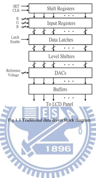
To coordinate with this pixel circuit, the data driver, simply demonstrated in figure 1.3, [2] plays an important role of signal translation. For displays with digital interface, the gray scales of pixels are fed in digital form and converted to analogue voltages in the data driver. After that, the analogue voltage is input and stored on the capacitors mentioned above. It requires reference voltages and resistor-string digital-to-analog-converter (R-DAC) with transmission gates to output the voltage level corresponding to a digital sub-pixel code [3]. In addition, the output buffers are indispensable to drive the highly capacitive data lines of the LCD panel. Therefore, all these parts of driving circuit cost a lot of area and power.
Nowadays, we have mature processing technology to improve TFT properties toward lower leakage current, higher mobility, and steeper sub-threshold swing. Some of those features are generally used to enhance TFT-LCD performances like aperture
2
ratio. Even with the much advancement in performance, it seems that the role of a TFT in the configuration of 1T1C circuit is nothing more than a gateway for capacitor charging. Thus, to make full use of the TFT, we think new pixel circuits can be designed to take more parts in the driving and share the burden of data driver.
Considering the fine sub-threshold swing, only a small voltage difference is enough to turn on and off a TFT. In other words, if we use the TFT as a dynamic switch to drive the pixel circuit, the power consumption may be lower than that of the traditional data driver.
Based on the new approach, this thesis proposes a new kind of pixel circuit, in which the pixel voltage is set by modulating the pulse width of data voltage on a TFT gate terminal to control the time of discharge through a resistor. As a result, the function of DAC is incorporated in the pixel. Therefore the R-DAC and output buffers in the data drivers can be omitted and the drivers become fully digital ones. Besides, for a data driver without the signal converting part will not only have lower production costs but also less power dissipation.
In order to verify that the proposed pixel circuit is suitable for displays in next generation, we need to successfully design display panels with it. The most popular applications of TFT LCDs are smart phones and large-area TVs. In these applications, for better visual experience, definition of 1920*1080, known as full high definition (FHD) [4], has become a basic specification of displays now. Furthermore, some newly HDTVs have already to support for video with definition up to 3840*2160 (which is named ultra-high definition, UHD). Therefore, two kinds of display panel, namely, 6-inch UHD and 65-inch 8k4k (FUHD) TV will be designed and simulated in this thesis.
3
1.2 Thesis Organization
After the introduction of chapter 1, this thesis analyzes both advantage and disadvantage of the novel pixel circuit compared with the conventional one under the cases of small and big size panel by simulating methods. Then, in chapter 2, we concern about issues of power dissipation and components tolerance such as threshold voltage (Vth) shift under the situation of small size panel. On the other hand, we look into the issues for the big size panel in chapter 3. Finally, we give a conclusion for results above in chapter 4. The section organization of the thesis is listed below:
Chapter 1 Introduction
1.1 Background and Motivation 1.2 Thesis Organization
Chapter 2 Proposed Pixel Circuit
2.1 Scheme and Operation 2.2 Features
2.2.1 Power on Data Bus 2.2.2 Charging Time
2.2.3 Gamma Correction and Number of Bits 2.3 Issues
2.3.1 Resistor in the Pixel 2.3.2 Aperture Ratio
2.3.3 Voltage Charging and Keeping 2.4 Improved Pixel Circuit
2.4.1 Scheme and Operation
4
3.1 Proposed Pixel Circuit
3.1.1 Design and Simulation 3.1.2 Design Tolerance 3.2 Conventional Pixel Circuit
3.2.1 Design and Simulating 3.2.2 Design Tolerance 3.3 Comparison
3.3.1 Panel Power Consumption 3.3.2 TFT’s Charging Capability 3.3.3 Aperture Ratio
3.4 Summary
Chapter 4 Large Size Panel
4.1 Proposed Pixel Circuit
4.1.1 Design and Simulation 4.1.2 Design Tolerance 4.2 Comparison
4.2.1 Panel Power Consumption 4.2.2 Aperture Ratio
4.3 Summary
Chapter 5 Conclusions and Future Works
5.1 Comparisons 5.2 Futures Works
5
Fig 1.1 Conventional pixel circuit array
6
7
Chapter 2
Proposed Pixel Circuit
2.1 Scheme and Operation
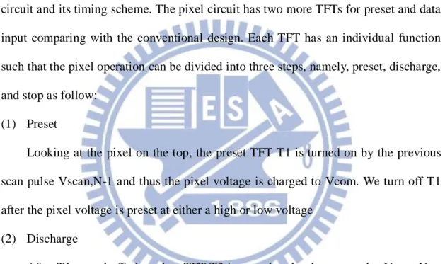
Figure 2.1(a) and (b) respectively show the proposed active matrix LCD pixel circuit and its timing scheme. The pixel circuit has two more TFTs for preset and data input comparing with the conventional design. Each TFT has an individual function such that the pixel operation can be divided into three steps, namely, preset, discharge, and stop as follow:
(1) Preset
Looking at the pixel on the top, the preset TFT T1 is turned on by the previous scan pulse Vscan,N-1 and thus the pixel voltage is charged to Vcom. We turn off T1 after the pixel voltage is preset at either a high or low voltage
(2) Discharge
After T1 turned off, the select TFT T2 is turned on by the scan pulse Vscan,N to enable the pixel. During this period of scan line, as the data voltage is set high, the pixel voltage starts to discharge through the resistor, T2, and the data TFT T3.
(3) Stop
When the pixel voltage comes to the expected value, the data voltage goes back to low to stop the discharge. In such a way, the pixel voltage can be driven by pulse width modulation of the data voltage.
Through the operation, the pixel voltage is kept on the capacitor and waits for the preset process of the next frame.
8
2.2 Features
2.2.1 Power on Data Bus
Figure 2.2 shows the typical characteristics of three kinds of TFTs. Taking a pixel resistance value as example, its corresponding current at a bias of 10V is indicated by the solid horizontal line in Figure 2.2. If the resistance of the TFT is higher or lower in one order of magnitude, as shown by the dotted lines, it can be taken as open or short compared to the pixel resistor. To provide this wide range of resistance control, the gate voltage swings for LTPS and IGZO TFTs are 1.3V and 6V respectively. Considering the threshold voltage shift, a wider voltage swing is needed. When the TFT is turned on, its resistance is much lower than that of the resistor. Therefore, most of the pixel voltage is across on the resistor. Even if the operating voltage of the liquid crystal is high, such as the blue phase liquid crystal, it does not affect the data control voltage and the power dissipated on the data bus is kept the same.
2.2.2 Charging Time
In the conventional LCD, the pixel voltage is targeting to the same voltage on the data bus. As the pixel voltage approaches the data voltage, the charging speed drastically slows down owing to the lowered TFT current. It takes much time to the charging for the last hundreds of minivolts, as shown in figure 2.3. As for the proposed method, we can over charge the pixel to a higher preset voltage and set the target voltage lower. By the early stop of the discharge before the speed getting slower,
9
the time to set the pixel voltage can be much shorten.
2.2.3 Gamma Correction and Number of Bits
The line time of an AM display is about 10s. Nanosecond step (GHz) [5] is good enough to divide the ON time in microseconds into a thousand steps, i.e., 10 -bit resolution. In such a case, the gamma correction can be dynamically implemented in the digital domain. Furthermore, the different gamma curves for red, green and blue can be separately adjusted, because they do not need to share the reference voltages.
2.3 Issues
2.3.1 Resistor in the Pixel
The implementation of the resistors in the pixel is the key issue of the proposed method. The resistance must be uniform in each pixel. This is really critical issue for this proposed method. However, this issue not a new problem in the field emission displays, and the solution of using boron-doped microcrystalline silicon was proposed [6]. The resistivity of the film is around 1.2x104-cm. Thus, a film with area of 5x5m2 and thickness of 500 nm is calculated to be 2.4 M. This film can be possibly filled in the contact hole with the process of lift-off, as shown in Fig.2.4. For the pixel capacitance of 1pF, the RC discharge time is about 7s, which is compatible to the line time.
2.3.2 Aperture Ratio
10
same role for charging. In this way, their size must be compatible to each other which results in a smaller aperture ratio for the novel design. Even though it can be observed that all the TFTs in proposed circuit are in series. Therefore, the layout can be neat and the aperture ratio of the pixel can still be high. The further comparisons will be conducted for the small and large area panels in Chapter 3 and 4.
2.3.3 Voltage Charging and Keeping
Although the circuit in figure 2.1(a) has conveyed our idea, after carefully looking into the operation, there are two critical drawbacks for the design. One is that after Vcom is stored in the capacitors as predicted, the pixel voltage changes with Vcom toggle for the voltage preset. Yet another issue is the charging capability of T1, since the charging time for the high definition display is limited. An improved version of the circuit is proposed in section 2.4 to fix these drawbacks.
2.4 Improved Pixel Circuit
2.4.1 Scheme and Operation
Figure 2.5(a) and (b) shows the improved pixel circuit with its timing scheme, respectively. In the circuit, T1 and T3 share Vscan,N-1 to finish preset and discharge steps respectively. Besides, a DC voltage source, namely, Vpre is used to replace precharge source Vcom in previous design. As a result, there is no more coupling problem. In the new circuit, the operation is also divided into three steps as described above. The differences will be illustrated in following statements.
11
TFT T1 is turned on by the previous scan pulse Vscan,N-1 and thus the pixel voltage is charged to Vpre. An advantage of this new design is that scan voltage can be turned high early to guarantee that pixel voltage will be preset to precise Vpre, since the precharging time can be very long before Vscan,N-1 turned off.
(2) Hold
When Vscan,N becomes high to preset pixel voltage in the next pixel it leads to both Vscan,N-1 and Vscan,N turn on simultaneously. Under this condition the pixel voltage is still keeping at Vpre since the operation voltage of Vdata isn’t high enough to open T3.
(3) Discharge
After T1 turned off, the select TFT T2 is turned on by the scan pulse Vscan,N to enable the pixel. During this period of scan line, as the data voltage is set high, the pixel voltage starts to discharge through the resistor, T2, and the data TFT T3. The improvement is that the reference voltage now equals to the low level of Vscan,N-1. In this configuration, we do not need to shift the level of Vdata to provide the proper gate-source voltage for T3 to be on or off. Thus, the operation of the data driver IC can be real low voltage.
(4) Stop
Again, when the pixel voltage comes to the expected value, the data voltage goes back to low to stop the discharge.
For the further inspection in the next chapters, we only apply this improved circuit in simulation to compare with the conventional design.
12
Fig 2.1(a) Proposed pixel circuit
13
Fig 2.2 Typical characteristics of three kinds of TFTs with their corresponding ON/OFF voltages
14
Fig 2.4 Cross-section of TFT with resistive film in the contact holes
15
16
Chapter 3
Small Size Panel
In this chapter, we do the simulation of a 6-inch UHD panel. Low-temperature poly-silicon (LTPS) TFT is used to construct the pixel circuit for its high mobility to enlarge the aperture ratio since the pixel size is very small. The basic specification is listed in table 3.1. The maximum liquid crystal capacitance (CLC,max) is set at a typical
value for the pixel size of this panel and storage capacitance (Cst) is set as large as
three times of the CLC,max. For small size TFT LCD panel, a 1-to-3 de-multiplexor is
commonly used to reduce the connection pin number [7]. Thus, here we also adapt this configuration, which makes the line time to be 2.5s.
Figure 3.1 shows the Id-Vg curve of level-62 RPI Poly-Si TFT model used in our simulation. The Vth is set at 1V with W/L equals to 5μm/5μm. Moreover, it is assumed that the maximum operating voltage of the liquid crystal is +/-5V. The design results for the proposed and conventional pixels will be compared after the simulation.
3.1 Proposed pixel Circuit
3.1.1 Design and Simulation
Since the pixel size is very small, the minimum size of the TFTs is used to enlarge the aperture ratio. Furthermore, the pixel size determines the pixel capacitance. For the proposed circuit, it is important to select the right value of the resistance R to
17
make sure the discharge can be completed in the limited line time.
In this design, the preset voltage is 10V and the target voltage of the discharge is set at -1V, while we only need the pixel voltage to stop at 0V at most. Therefore, the discharge range is about 10V/11V, or 91%. The exponential discharge of 91% corresponds to the 2.3 times of the time constant. For the line time of 2.5s, time constant should be 1.1s. Thus, for the pixel capacitance (CLC,max+ Cst) of 40fF, we
need the resistance to be 27M.
The scan voltages are set to be the same as the conventional ones for the later comparison. The on and off voltage of the data line should be properly decided to make the resistance low and high enough compared to R, respectively. Its tolerance to the Vth shift must be also considered but yet to be verified. Table 3.2 summarizes the design results of the proposed pixel, including device sizes and voltage levels.
This simulation results are shown in figure 3.2. In the figures, Vpix is initially set to 10V in period I when Vscan1 is high. In period II, it is confirmed that the preset voltage is not affected by the simultaneous high level of Vscan1 and Vscan2. In period III, Vscan1 goes to low level, so that, the pixel voltage starts to discharge. For
figure 3.2 (a), (b), and (c), the discharge stops at 10V, 5V and 0V, respectively. With
Vcom set around 5V, the voltages across the liquid crystal are set to be 5V, 0V and -5V, accordingly. From these results, we demonstrate that the proposed circuit is functional.
3.1.2 Design Tolerance
In this section, we verify the effect of Vth shift on the proposed pixel. The simulation of figure 3.2 (a) is redone with Vth to shift +0.5V and -0.5V from 1V for each TFT in the proposed pixel. It is found that the Vth shift for T1 and T2 does not
18
affect the Vpix at all. As for T3, the Vpix deviates about 10mV from the target voltage of 0V when Vth shifts +0.5V, as shown in figure 3.3. The error ratio is only 1/1000 to the full swing of 10V. As for the negative Vth shift, there is no problem because of the better discharge capability.
3.2 Conventional Pixel Circuit
3.2.1 Design and Simulation
The 1T1C pixel circuit is used as reference to be compared with the proposed circuit. Figure 3.4(a) and (b) show the conventional circuit and its timing scheme, respectively. The operation parameters for this circuit are listed in table 3.3. The simulated waveform of the pixel voltage is shown in Figure 3.5, along with the data and scan voltages. It can be seen that the pixel voltage is successfully charged to 10V within 2.5μs.
3.2.2 Design Tolerance
Vth shift issue is also checked for the conventional pixel in this section. The simulation in figure 3.5 is repeated with the Vth shift to verify the design tolerance. Figure 3.6 shows that if Vth shifts 0.5V higher, TFT is barely able to charged pixel voltage to the target voltage of 10V. In this case, the deficiency of Vpix is about 50mV. As for the negative Vth shift, there is no problem, either. We will use this design for the comparison in the next section.
19
Besides the advantage of the digital driving, we here compare the proposed and conventional circuits in other aspects. Such as power consumption, aperture ratio, and charging capability.
3.3.1 Panel Power Consumption
The power issue is always a big challenge for small display panels. For an UHD conventional design, the OP with a usual 2A bias current in the 2160 channels of the data driver dissipates DC power about 21.6mW. In addition, the usual Gamma resistance of 100k in the R-DAC for the 10V operating voltage dissipates DC power of 1mW. On the contrary, the proposed structure has no more OP AMPs and R-DACs so that the DC power dissipation can be totally saved.
Furthermore, we bring the dynamic power consumption on the data buses into comparison [8]. For the proposed design, the frequency of data source voltage switching is twice as the conventional one. However, the voltage swing is much reduced. For example, if the total capacitance loading on data line is 20pF then the overall power dissipation is calculated to be as low as 0.24W. As for the conventional design, the power is estimated to be 1.5W. In addition to the DC power, the dynamic power consumption is also greatly reduced in the proposed panel.
3.3.2 TFT’s Charging Capability
The size of T1 in proposed circuit was expected to be the same as that in conventional pixel circuit. However, the simulation results illustrate the new design has a better charging capability, since the pre-charging period can be extended. Therefore, it’s an expected advantage that we do not need to raise T1’s size even the
20
line time is very short in a higher definition display. In the discharging path, T2 is used as a switch in connection with scan line to select the pixel, while T3 dominates the discharging period.
It is the value of R but not T2 and T3 to decide the discharge speed, as long as the on and off resistances of T2 and T3 are very much lower and higher than R, respectively. The charging capability of TFTs in the proposed circuit is less important as it is in the conventional pixel.
To demonstrate the ineffectiveness of TFT charging capability, we shorten the line time to 1.5s and redo the simulation. The result is shown in Figure 3.7. All the parameters including the sizes of T1, T2, and T3 are kept the same except that R is reduced to a smaller value to correspond to the shorter line time. The full swing of pixel voltage illustrates that irrelevance of the TFT size. It also reveals that the proposed pixel circuit is ready to support the display with the even shorter line time.
3.3.3 Aperture Ratio
Aperture ratio will be found out from the layout scheme. Figure 3.8(a) and (b) show the schemes of conventional and novel circuits respectively. For the conventional design, the aperture ratio is about 47.73%. However, the novel design has only 31% which is lower than the conventional one as estimated.
3.4 Summary
The simulation results prove that the proposed pixel circuit can successfully operate with the whole digital signal sources. The circuit has good tolerance to Vth degradation. Benefiting from the fine sub-threshold swing of LTPS TFT, the dynamic
21
power consumption on data line is much less than conventional one. Despite of the smaller aperture ratio, the proposed pixel circuit is applicable in a high definition display with pixel per inch as high as 769.7.
22
Fig 3.1 Id-Vg curve of LTPS TFT model
(a) 1.00E-11 1.00E-10 1.00E-09 1.00E-08 1.00E-07 1.00E-06 1.00E-05 1.00E-04 1.00E-03 1.00E-02 -5 -3 -1 1 3 5 7 9 11 13 15 17 19
Id
(A
)
Vgs(V)
Vth=1V
-2 0 2 4 6 8 10 12 14 16 0 2 4 6 8 10 12 14 16 18 20V
o
lt
a
ge
(V
)
Time (us)
Vdata Vscan,N-1 Vscan,N Vpix I II III23
(b)
(c)
Fig 3.2 Simulation result of the proposed pixel with the pixel voltage set at (a)0V (b)5V and (c)10V -2 0 2 4 6 8 10 12 14 16 0 2 4 6 8 10 12 14 16 18 20
V
ol
ta
ge
(
V
)
Time (us)
Vdata Vscan,N-1 Vscan,N Vpix -2 0 2 4 6 8 10 12 14 16 0 2 4 6 8 10 12 14 16 18 20V
ol
ta
ge
(
V
)
Time (us)
Vdata Vscan,N-1 Vscan,N Vpix24
Fig 3.3 Worst case under the condition of Vth shift
Fig 3.4 (a) 1T1C pixel circuits in column series
-2 0 2 4 6 8 10 12 14 16 0 2 4 6 8 10 12 14 16 18 20
V
ol
ta
ge
(
V
)
Time (us)
Vdata Vscan,N-1 Vscan,N Vpix_Vth=1V Vpix_Vth=0.5V Vpix_Vth=1.5V25
Fig 3.4 (b) Driving scheme of 1T1C pixel circuits
Fig 3.5 Simulation result of conventional pixel circuit
-2 0 2 4 6 8 10 12 14 16 0 2 4 6 8 10 12 14 16 18 20
V
ol
ta
ge
(
V
)
Time (us)
Vdata Vscan,N Vpix26
Fig 3.6 Simulation result for 1T1C with Vth shift
Fig 3.7 Simulation result with 1.5s line time
-2 0 2 4 6 8 10 12 14 16 0 2 4 6 8 10 12 14 16 18 20
V
ol
ta
ge
(
V
)
Time (us)
Vdata Vscan,N Vpix_Vth=1V Vpix_Vth=0.5V Vpix_Vth=1.5V -2 0 2 4 6 8 10 12 14 16 0 1 2 3 4 5 6 7 8 9 10V
ol
ta
ge
(
V
)
Time (us)
Vdata Vscan,N-1 Vscan,N Vpix27
Fig 3.8(a) Layout of conventional pixel
28
Table 3.1 Specification for small size panel
6-inch UHD
Specification
Orientation
Portrait
Frame Rate
60Hz
Resolution
2160 x 3840
Pixel Size
11μm x 33μm
C
10fF
C
30fF
Demux
1 : 3
Line Time
2.5μs
Table 3.2 Design result of the proposed pixel
Novel design
Value
Vcom
5V
Vpre
10V
R
27MΩ
Vdata on/off
5V / 1V
Vscan on/off
13.5V / -1V
T1 W/L
5μm / 5μm
T2 W/L
5μm / 5μm
T3 W/L
5μm / 5μm
29
Table 3.3 Design result of the conventional pixel
Conventional design
Value
Vcom
5V
Vdata on/off
10V / 0V
Vscan on/off
13.5V / -1V
30
Chapter 4
Large Size Panel
In this chapter, we want to verify the operation of proposed pixel circuit in the case of 65-inch FUHD display. The pixel circuit will be constructed by Indium gallium zinc oxide (IGZO) TFTs. The IGZO TFT has advantages of less masks process than LTPS TFT and high carrier mobility, compared to amorphous Silicon (a-Si) TFT. As a result, IGZO TFT is suitable for pixel circuit in large scale display. In Figure 4.1 shows the simulated Id-Vg curve of level-61 RPI a-Si TFT model which is used to imitate the properties of IGZO TFT. The Vth of the curve is set at 1V with W/L equals to 5μm/5μm. The maximum operating voltage of the liquid crystal is also assumed to be +/-5V as before.
Basic specification for large size display is listed in table 4.1. As listed in the table, CLC,max is set at 0.1pF and Cst is three times larger than CLC,max. Without the
cooperation of Demux, the line time is raised to 3.5s in this case.
For a large scale display, the signal usually gets distorted after a high frequency pulse transmiting over the long bus with the resistance and parasitic capacitance. Therefore the driving sources for pixel circuit in this chapter are transformed into trapezoidal wave to prevent that error [9]. Figure 4.2(a) and (b) show the tolerance for the RC delay of square and trapezoidal waves, respectively. In the figures, the output of square wave is obviously out of shape which can lead to the non-uniformity in the display and is not acceptable. In order to prevent the distortion, we then set the rising/falling periods of scan and data source to be 1.5s and 1s respectively.
31
4.1 Proposed Pixel Circuit
4.1.1 Design and Simulation
In this design, the scan voltages are set to be the same as the conventional ones for the later comparison. The preset voltage is 22V and the target voltage of the discharge is set at -5V which equals the off voltage level of scan line. While we only need the pixel voltage to stop at 12V at most, such discharging range can avoid the slow discharging period. The exponential discharge from the preset of 22V to the target of 12V takes only the 0.5 times of the time constant. For the line time of 3.5s, time constant can be set at 3.5s. Thus, for the pixel capacitance (CLC,max+ Cst) of
0.4pF, we need the total resistance in the discharging path to be 17M. However, the data signal is a trapezoidal wave, which means the TFT cannot be turned on instantaneously. In other words, the total line time is less than 3.5s. As a result, the pixel voltage cannot reach 12V in time, as shown in Figure 4.3. Therefore the resistance is finally reduced to 14M to meet the shorten discharging period.
Table 4.2 summarizes the design results of the proposed pixel, including device sizes and voltage levels. The simulation results are shown in figure 4.4. In the figures, Vpix is initially set to 22V in period I when Vscan1 is high. In period II, it is confirmed that the preset voltage is not affected by the simultaneous high level of Vscan1 and Vscan2. In period III, Vscan1 goes to low level, so that, the pixel voltage starts to discharge. For figure 4.4 (a), (b), and (c), the discharge stops at 22V, 17V and 12V, respectively. With Vcom set around 17V, the voltages across the liquid crystal are set to be 5V, 0V and -5V, accordingly. From these results, we demonstrate that the proposed circuit is also working well in large scale display.
32
4.1.2 Design Tolerance
To verify the Vth shift tolerance of proposed circuit, the simulation of figure 4.4(a) is redone with Vth to shift +0.5V and -0.5V from 1V for each TFT in the pixel. It is found that the Vth shift for T1 and T2 does not affect the Vpix at all. However, for the Vth shift in T3, the Vpix deviates about 0.6V from the target voltage of 12V. Figure 4.5 shows that the error appears when Vth shifts in both positive and negative ways.
With further analysis, we found that it is attributed to the undetermined off time in the trapezoidal wave owing to the Vth shift. For example, T3 with smaller Vth will be turned on faster than the normal one in the rising period of the data voltage, and it will be closed slower in the falling period. In such a way, Vth shift of T3 changes the discharging period length and thus the pixel voltage.
To alleviate the error we can intuitively reshape the data source with a steeper edge. Figure 4.6 shows that the proposed circuit has better tolerance to Vth shift of T3 after the rising/falling edge of data source were reduced to 0.5s. However it is not a practical method because high-frequency component put back into the signal source will be still filtered away by the bus.
There is another proper way to solve the problem. Since the proposed pixel is driven by the full digital signals, it is possible to compensate the pixel voltage from outside. The process is briefly described in following statements. At first, the gray levels of each pixel corresponding to different data pulse widths are detected and stored in the memory. Then for every frame, the digital data signals are compensated by adding or subtracting the data in memory before delivered to the data driver. As a result, the Vth shift effect of T3 on the discharging period length can be ameliorated. This solution takes advantage of the full digital driving scheme.
33
4.2 Comparison
4.2.1 Panel Power Consumption
In this section we compare the power consumption between conventional and novel design again. For a conventional 8k4k display, without Demux the OP with a 2A bias current in data driver dissipates about 64.8mW. On the contrary, the proposed structure has no more OP AMPs and R-DACs so that the DC power dissipation can be totally saved.
Furthermore, we bring the dynamic power consumption on the data buses into comparison. For the proposed design, the frequency of data source voltage switching is twice as the conventional one. However, the voltage swing is half time to the conventional one. Therefore if the total capacitance loading on data line is 40pF then the display power dissipation is calculated to be 2.98W. But for the conventional design, the power is estimated to be 11.98W. In addition to the DC power, the dynamic power consumption is also reduced in the proposed panel.
4.2.2 Aperture Ratio
Aperture ratio will be found out from the layout scheme. Figure 4.7(a) and (b) show the schemes of conventional and novel circuits respectively. For the conventional design, the aperture ratio is about 79.38%. However, the novel design has only 65.89% which is lower than the conventional one as estimated.
34
4.3 Summary
From the simulation results the proposed pixel circuit can successfully operate in the case of big size display. It dissipates lower power than conventional 1T1C pixel circuit. Besides, benefiting from full digital driving, we can solve the voltage setting error owing to Vth shift by compensating data signal externally. Despite of the slightly smaller aperture ratio, the proposed pixel circuit can still be applied in a high definition display with pixel per inch as high as 135.6.
35
Fig 4.1 Id-Vg curve of IGZO TFT model
(a) 1.00E-12 1.00E-11 1.00E-10 1.00E-09 1.00E-08 1.00E-07 1.00E-06 1.00E-05 1.00E-04 -5 -3 -1 1 3 5 7 9 11 13 15 17 19
Id
(A
)
Vgs(V)
Vth=1V
-2 0 2 4 6 8 10 12 0 3 6 9 12 15V
o
lt
age (
V)
Time (us)
Vin Vout36
(b)
Fig 4.2 Tolerance for the RC delay of (a) square and (b) trapezoidal waves
Fig 4.3 Simulation result with R equals to 17M
-2 0 2 4 6 8 10 12 0 3 6 9 12 15
V
o
lt
age (
V)
Time (us)
Vin Vout -10 -5 0 5 10 15 20 25 30 0 2 4 6 8 10 12 14 16 18 20V
ol
ta
ge
(
V
)
Time (us)
Vdata Vscan,N-1 Vscan,N Vpix37 (a) (b) -10 -5 0 5 10 15 20 25 30 0 2 4 6 8 10 12 14 16 18 20
V
o
lt
a
ge
(V
)
Time (us)
Vdata Vscan,N-1 Vscan,N Vpix -10 -5 0 5 10 15 20 25 30 0 2 4 6 8 10 12 14 16 18 20V
ol
ta
ge
(
V
)
Time (us)
Vdata Vscan,N-1 Vscan,N Vpix I II III38
(c)
Fig 4.4 Simulation result of the proposed pixel with the pixel voltage set at (a)12V (b)17V and (c)22V
Fig 4.5 Worst case under the condition of Vth shift
-10 -5 0 5 10 15 20 25 30 0 2 4 6 8 10 12 14 16 18 20
V
ol
ta
ge
(
V
)
Time (us)
Vdata Vscan,N-1 Vscan,N Vpix -10 -5 0 5 10 15 20 25 30 0 2 4 6 8 10 12 14 16 18 20V
ol
ta
ge
(
V
)
Time (us)
Vdata Vscan,N-1 Vscan,N Vpix_Vth=1V Vpix_Vth=0.5V Vpix_Vth=1.5V39
Fig 4.6 Data voltage with a steeper edge
Fig 4.7(a) Layout of conventional circuit
-10 -5 0 5 10 15 20 25 30 0 2 4 6 8 10 12 14 16 18 20
V
ol
ta
ge
(
V
)
Time (us)
Vdata Vscan,N-1 Vscan,N Vpix_Vth=1V Vpix_Vth=0.5V Vpix_Vth=1.5V40
41
Table 4.1 Specification for large size panel
65-inch FUHD
Specification
Orientation
Landscape
Frame Rate
60Hz
Resolution
7680 x 4320
Pixel Size
58μm x 173μm
C
0.1pF
C
0.3pF
Line Time
3.5μs
Table 4.2 Design result of the proposed pixel
Novel Design
Value
Vcom
17V
Vpre
22V
R
13MΩ
Vdata on/off
1.5V / -3.5V
Vscan on/off
27V / -5V
T1 W/L
5μm / 5μm
T2 W/L
5μm / 5μm
T3 W/L
10μm / 5μm
42
Chapter 5
Conclusions and Future Works
5.1 Conclusions
To save power dissipation and cost of LCD, the pixel circuit with full digital signal driving is newly invented. In the proposed scheme, the R-DAC and output buffers in the conventional data drivers can be omitted. The operation of the novel circuit is verified by simulation for both small and large size panels. The results show that dynamic power consumption is obviously low, compared to conventional 1T1C configuration. Moreover, the proposed pixel circuit has high tolerance for Vth shift in the case of small size display. Despite of the smaller aperture ratio, the proposed pixel circuit can still be applied in a high definition display with high PPI. In the application of large panel, the driving signals are set to be trapezoidal waveforms to prevent propagation distortion. For the problem of pixel voltage setting owing to Vth shift, we can easily solve it by compensating each pixel from outside. It takes advantage of the full digital driving scheme.
5.2 Future Works
For the next step, we expect to finish the circuit on the breadboard to verify the circuit with the actual operation. In addition, the implementation of the resistance in pixel needs to be explored. Besides, finding better layout method to increase aperture is necessary.
43
References
[1] B. J. Lechner, F. J. Marlowe, E. O. Nester, and J. Tults, “Liquid crystal matrix displays,” Proc. of the IEEE, Vol. 59, pp. 1566–1579, 1971.
[2] C. W. Lu, “TFT-LCD Driver IC Design, New Developments in Liquid Crystals,” Georgiy V Tkachenko (Ed.), 2009, ISBN: 978-953-307-015-5
[3] K. Takahara, T. Yamaguchi, M. Oda, H. Yamaguchi, T. Aoki, F. Asami, “Data driver circuit of liquid crystal display for achieving digital gray-scale,” United States Patent US5196738 A, 1993.
[4] “Graphics display resolution,” Wikipedia: The Free Encyclopedia, Wikimedia Foundation, Inc., Retrieved 14 June 2014,
<http://en.wikipedia.org/wiki/Graphics_display_resolution>
[5] Goldberg, J. M.; Sandler, M.B., "New high accuracy pulse width modulation based digital-to-analogue convertor/power amplifier," Circuits, Devices and Systems, IEE Proceedings , vol.141, no.4, pp. 315-324, Aug 1994
[6] D. A. Cathey, Jr., K. W. Tjaden, B. Moradi, J. K. Lee, and J. J. Alwan, “Light-insensitive resistor for current-limiting of field emission display,” United States Patent 6,507,329 B2, 2003.
[7] J. C. Yeo, S. G. Kim, “Liquid crystal display and driving method thereof,” United States Patent US 7084844 B2, 2006.
[8] “CMOS,” Wikipedia: The Free Encyclopedia, Wikimedia Foundation, Inc., Retrieved 14 June 2014, < http://en.wikipedia.org/wiki/CMOS>
[9] R. V. Balakrishnan, W. R. Fowler, “Data bus transceiver,” United States Patent US4320521 A, 1982.