國 立 交 通 大 學
電子工程學系 電子研究所
博 士 論 文
分離式閘極非揮發性記憶體技術及
新穎多晶矽電子抹除式唯讀記憶體之研究
Study on Split-Gate Non-Volatile Memory
Technology and A Novel Single Poly EEPROM
Memory Cell
研 究 生 :宋 弘 政
指導教授 :雷 添 福
分離式閘極非揮發性記憶體技術及
新穎多晶矽電子抹除式唯讀記憶體之研究
Study on Split-Gate Non-Volatile Memory Technology and
A Novel Single Poly EEPROM Memory Cell
研究生:宋 弘 政
Student:Hung-Cheng Sung
指導教授:雷添福 博士
Advisor:Dr. Tan-Fu Lei
國立交通大學
電子工程學系 電子研究所
A Dissertation
Submitted to Department of Electronics Engineering
and Institute of Electronics
College of Electrical and Computer Engineering
National Chiao Tung University
In Partial Fulfillment of the Requirements
For the Degree of
Doctor of Philosophy
In
Electronics Engineering
June 2008
Hsinchu, Taiwan, Republic of China
中華民國九十七 年 六 月
分離式閘極非揮發性記憶體技術 及
新穎多晶矽電子抹除式唯讀記憶體之研究
學生: 宋 弘 政
指導教授: 雷 添 福 博士
國立交通大學
電子工程學系 電子研究所博士班
摘
要
在此論文,首先,我們發展了一種新的方法來作分離式閘極快閃記憶體的寫 入及干擾空間的量測。這個方法能幫助我們定量地了解操作空間的變化與電壓的 關係,進而,這方法可以用來找到最佳化的寫入條件。由此方法找到的條件可以 承受最大的電壓變化。我們成功地運用這方法在新一代的分離式閘極快閃記憶體 的發展。 再者,一種新穎的三重自動對準分離式閘極快閃記憶元在此論文被揭露。此 記憶元有 T 型的耦合結構,此新結構能大幅地增加源極和浮動閘極間的耦合電容7.4V降至 6.4V。而對於記憶元的縮小,我們成功地降低浮動閘極的長度由 0.18µm 到 0.14µm 而沒造成良率的下降或者可靠度的衰退。 最後,一種有著金屬控制閘極的新穎單多晶矽電子抹除式唯讀記憶體 EEPROM 在此論文中被發表。它的金屬閘極是由嵌刻(damascene)製程作成的鎢 (W)線,它的閘極間的介電層是由原子磊晶長成的氧化鋁(Al2O3)。它的寫入/抹除 的操作方式和傳統的堆疊閘極(stack-gate)記憶元是相同的,它用通道熱電子注入 做寫入及用 FN 穿隧做抹除。因氧化鋁有著高介電常數的特性,所以我們可以用 小於 6.5V 的電壓來執行寫入及抹除,而此電壓可以用 3.3V 的元件來操作,而不 用使用到傳統的高壓元件。在製程相容方面,此記憶體只需比傳統 CMOS 製程 多出二道光罩既可,此外,這氧化鋁是在後段製程中完成,所以此技術沒有汙染 的顧慮以及額外高溫製程所造成的元件影響。因此,此技術非常能適用於嵌入式 產品的應用。在此論文中,我們發表了良好的記憶體特性,如快速的寫入及抹除 還有良好的重覆寫入/抹除特性及資料持久性。
Study on Split-Gate Non-Volatile Memory
Technology and A Novel Single Poly EEPROM
Memory Cell
Student: Hung-Cheng Sung
Advisor: Dr. Tan-Fu Lei
Department of Electronics Engineering &
Institute of Electronics
National Chiao Tung University
ABSTRACT
In this thesis, first, we developed a new methodology for program vs disturb
window characterization on split gate flash. This method can help us to understand
quantitatively how the window shifts vs bias conditions; furthermore, find the optimal
program condition. The condition obtained by this method can withstand the largest
program bias variations. This methodology was successfully implemented in the
development for new generation of split-gate cell
significantly enhance coupling capacitance between the source and floating gate
without increasing cell size. The enhancement can be simply modulated by an
oxide-etching step. This new structure can be applied to program voltage reduction
and cell size scaling. For program voltage reduction, the maximum program voltage
of the new cell can be reduced from 7.4 to 6.4 V. For cell size scaling, we successfully
reduce the floating length from 0.18µm to 0.14µm without showing the yield loss or
reliability degradation.
Finally, a novel single poly EEPROM with metal control gate structure is
presented in this paper. The control gate is tungsten (W) line made by a damascene
process, and inter-gate dielectric is Al2O3 grown by Atomic Layer Deposition (ALD).
The program and erase mechanism is the same as the one for traditional stacked-gate
cell, which uses the channel hot electron injection for programming and
Fowler-Nordheim (F-N) tunneling for channel erasing. With the high dielectric
constant (K) property of Al2O3, we can perform the program and erase function with
a voltage less than 6.5 V, which can be handled by 3.3 V devices instead of traditional
high voltage devices. In the process compatibility aspect, this new cell needs only two
deposited in the back-end metallization steps, so there is no cross-contamination issue
caused by new material nor the device impact induced by the extra thermal cycle from
conventional double poly process. Therefore, this new technology is suitable for
embedded application. In this paper, the good cell performance is demonstrated; such
誌謝
首先我要向我的指導教授雷添福博士致上最高的敬意。感謝他在學業研究與 生涯規劃上給我的指導與鼓勵。此外,我要感謝台積電的王中樞資深處長和林詠 濤處長的栽培和幫助、以及非揮發性記憶體部門同仁在技術方面的討論和建議, 令我獲益良多。 同時也要感謝實驗室裡學弟的幫忙,你們的協助讓我的論文能順利完成。 最後,要感謝父母親多年的辛苦栽培以及我可愛的妻子和女兒的鼓勵。僅此 論文獻給所有關心我的朋友。Contents
Abstract (Chinese) ………I Abstract (English)………..III Acknowledge ………..VI Contents ………....VII Figure Captions ………..……….... X
Chapter 1 Introduction ………..……….1
1.1 Embedded Flash Market and Application ………..…..………...1
1.2 Embedded Flash Technologies………..……...3
1.2.1 1T Stack-gateTechnologies………..……...3
1.2.2 Split-gateTechnology ……….……..……...4
1.2.3 2T Stack-gateTechnology ……….……….……..……...5
1.2.4 Fully overlap Stack-gateCell……….……….……..……...6
1.3 Purposeofthiswork ……….………..6
Reference……….…………..20
Chapter 2 Split-GateFlash Operation……….... 22
2.1 Introduction ……….………...…..22
2.2 Cell cross-section and Layout...………...………..22
2.3 CellArray Schematic ………….………..22
2.4 Programming ………….………..23
2.5 Erasing ..……….………..26
Chapter 3 Novel Program vs Disturb Window Characterization for Split-Gate
Flash Cell ………..……….... 36
3.1 Introduction ……….………...…..36
3.2 Experiment...………...………...………..37
3.3 Program vs.Disturb Window Characterization ………..38
3.4 Application oftheWindow Characterization ………..41
3.4.1 Finding optimalprogramming condition ……….…………..41
3.4.2 Constant voltage vs. constant currentprogramming ………..41
3.5 Summary……….……….…42
Reference……….……….…57
Chapter 4 New Triple Self-aligned (SA3) Split-Gate Flash Cell with T-Shaped SourceCoupling …….……….…..58 4.1 Introduction………..58 4.2Devicefabrication………….………..………..59 4.3 Array Biascondition ………..………..60 4.4 TheSCR Effecton Program and Erase..……….60 4.4.1 Programming .………...60 4.4.2 Erasing ………...………..60
4.5 Application to VoltageReduction ..……….…..………...61
4.6 Application to CellSizeReduction ..……….…..……….……...62
4.7 Summary ..……….…………...……...63
Reference..……….…………..…..……...73
Chapter 5 Novel Single Poly EEPROM with Metal Control Gate Structure..75
5.2 DeviceFabrication…..……….………..………..76
5.3 Resultand Discussion………...77
5.4 Conclusion ………...79
Reference..……….………...88
Chapter 6 Conclusionsand FurtherRecommendations……….…...90
6.1 Conclusions……….………....90
6.2 Furtherrecommendations…………..……….………..…91
Reference………..………....94
Vita ……….……..………..………....95
Figure Captions
Chapter 1
Fig. 1.1 (a)Estimate from 2004 to 2010 for unit shipments of flash MCU chips. (b) Flash MCU characteristics and memory density by application type. ……..9 Fig. 1.2 Rapid increasing numbers of microcomputers are used in vehicles. The latest carshavemicrocomputersin from 30 to 100 differentlocations.………..10 Fig. 1.3 (a) Schematic cross sectional view of stacked gate Flash memory cell along
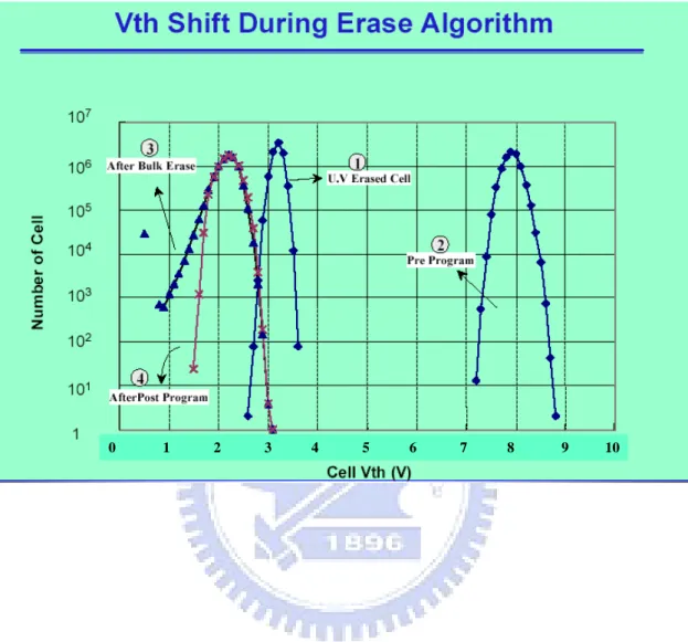
cell channel direction. The programming is through hot electron on drain side and erase is accomplished by FN tunneling in source side. (b) Top view and cross sectional view along with direction of stacked gate Flash memory cells fabricated in 0.35-mm technology.………..… 11 Fig. 1.4 (a) Threshold voltage distribution of a 1-Mb Flash array after UV erasure,
after CHE programming, and after FN erasure. (b) In NOR array architecture, the leaky bit can cause the read failure on its bit line [4]. ……… 12 Fig. 1.5 VT shift during erase algorithm. A soft program after bulk erase can
effectively tighten up the VT distribution.………..… 13 Fig. 1.6 Schematic illustration of self-aligned split-gate Flash cell (SuperFlash®)
proposed by SST ………..14
Fig. 1.7 (a) Schematic of split gate nano-crystal bit cell for control gate-first and select gate-first integrations by Freescale, (b) Cell structure of MONOS split gate flash memory by Renesas, (c) Technology roadmap of Embedded Flash
MCU by Renesas.……….15
Fig. 1.8 (a) 2-Trstack gateNOR cellstructure,(b)Top view ofthecell[12]………16 Fig.1.9 Schematicdiagram oftheoperation of2 Trstack gatecell.……….17
Fig. 1.10 Top and cross-section drawing ofthefully overlap cell……… 18 Fig. 1.11 (a) Circuit schematic drawing, (b) The operating conditions for word
rewritablearray ……… 19
Chapter 2
Fig. 2.1 (a) Cross-section of triple self-aligned split-gate Flash cell in bit-line direction, (b)Schematicdiagram ofcelltop view and array configuration.………..28 Fig. 2.2 (a) Equivalent circuit of split-gateFlash cell,(b)Cellarray schematic… 29 Fig. 2.3 Bias condition and advantage of split-gate Flash cell. ……….30 Fig. 2.4 Simulation results of the lateral field distribution along channel surface for
(a) region-A (b) region-B (c) region-C. The enlarged schematic cross-section with electron flow lines during programming is shown in (b). In the inset of (b), point A (or A’) marks the physical boundary between SG (or FG) and IPO. Point G (or G’) marks the position of the maximum lateral field. The device parameters are: LSG= 0.3m, LFG= 0.183m, LFG= 0.4
m, TSGOX = 180 Å, TFGOX = 100 Å.………..31
Fig. 2.5 (a) Pinch-off point of FG and SG is A and B, respectively. Electron injection point is C, where is located in floating gate edge on the poly space. (b) Electricfield and electron injection probability distribution.……….32 Fig. 2.6 (a) Magnification of poly tip for tunneling, (b) energy band diagram during
erasing, Emax is near the poly tip due to field-enhanced effect.………… 33
Chapter 3
sharp FG corner (indicated by the circle) created by poly etch.………….44 Fig. 3.3 Cell array and bias voltage for program, erase, read-out and three disturb conditions, which are: A. Column punchthrough disturb(PTC), B. Row punchthrough disturb(PTR), C. Reverse tunneling disturb(RT). Note that the cellsoutsidetheselected pageareimmunefrom disturb stress.………… 46 Fig. 3.4 Program vs disturb window and the operation circle. The programming time is 10us and program currentis5μA. ……… 47 Fig.3.5 Program trend in PGM vsDisturb window.……… 48 Fig. 3.6 Bias condition for Column punch-through (PTC)and thedisturb trend.… 49 Fig. 3.7 Bias condition for Row punch-through (PTR) and the disturb trend ………50 Fig.3.8 Biascondition ofReversetunneling (RT)and thedisturb trend …………..51 Fig.3.9 Trend ofVdp in operation window plot……… 52 Fig. 3.10 Operation circle in program and disturb window. The optimal program
condition is at circle center, the condition is VSS=7.2V, Vg=1.75V,
Idp=5μA.………...53
Fig. 3.11 (a) Program vs disturb window varies with Idp from 1,5 to 9uA. Since the channel doping is well adjusted in this SA3 cell, no significant disturb boundary shift is observed under Idp variation (b) Operation circle comparison between Idp=1,5,9 μA.Theoptimalprogram condition ischosen atr2 center(Idp=5μA)becauseithaslargestoperation circle,thecondition is VSS=7.2V,Vg=1.75V,Idp=5μA.……….54 Fig. 3.12 The circuit diagram for constant current and constant voltage
programming ………..55
Fig. 3.13 (a) The overlap window for constant current programming. The Idp varies from 1uA to 9uA, (b) The overlap window for constant voltage programming.Th eVdp variesfrom 0V to 0.6V.……… 56
Chapter 4
Fig. 4.1 The cell cross-sectional view of tradition non-self-aligned cell vs. triple self-aligned(SA3)cell.………..64 Fig. 4.2 Process flow of the T-shaped Triple Self-aligned (SA3) split-gate flash
cell.……… 65
Fig. 4.3 (a) Traditional SA3 vs. T-shaped Vss coupling SA3 cell. (b) TEM picture of thenew cell.Thecellsizeis0.38 µm2.……… 66 Fig. 4.4 Cell array and bias voltage for program, erase, read-out and three disturb conditions, which are: A. Column punchthrough disturb(PTC), B. Row punchthrough disturb(PTR), C. Reverse tunneling disturb(RT). Note that the cells outside the selected page are immune from disturb stress.………….67 Fig. 4.5 (a) Pinch-off point of FG and SG is A and B, respectively. Electron injection point is C, where is located in floating gate edge on the poly space. (b) Electric field and electron injection probability distribution (c) Plot of factors effect on the electron injection probability. The factors include source voltage (Vss), source coupling ratio (SCR), substrate bias (Vsb) and bit-line
voltage( Vbl).……….68
Fig. 4.6 Source coupling ratio (SCR) vs. FG oxide spacer pull-back etching.…… 69 Fig. 4.7 (a) Program improvement vs FG oxide spacer pull-back. The program
performance is characterizaed by Ir0/Ir1@Vs=6V, 10us, program current=3uA, where Ir0 and Ir1 is programmed and erased current, respectively. (b) Erasing improvement vs. FG oxide spacer etching. The
Fig. 4.8 (a) Program vs. disturb window of traditional SA3 cell. The source voltage for programming is 7.4V, (b) Program vs. disturb window of T-shape Vss coupling SA3 cell.Vssvoltagecan bereduced to 6.4V in new cell.…….71 Fig. 4.9 FG length reduction vs. yield. The yield of new SA3 cell remains stable when
FG length is reduced, whereas the yield of old SA3 cell drops drastically with the shorter FG length. Note that the nominal FG length is around 180nm. . 72
Chapter 5
Fig. 5.1 (a) Logic OTP using oxide rupture mechanism [2]. The capacitor shown in the figure is a poly gate with junction overlap structure, it can be breakdown during programming, (b) schematic diagram of device and array structure for a single PMOS logic OTP memory [3], (c) The top and cross
section view of eFuse. ……… 80
Fig. 5.2 Schematic diagram and cross-sectional view of a logic MTP memory. ….81 Fig. 5.3 (a) Cross-sectional view of a single cell, (b) Top view cell layout. The ideal
2T and 1T cellsizeis26F2 and 18F2,respectively.……… 82 Fig.5.4 TEM picture of final cell. A proper oxidation treatment (~1 nm) before ALD
and a post ALD anneal were done to ensure a good inter-gate dielectric quality. The physical thickness and the equivalent oxide thickness (EOT) of Al2O3 isabout20 nm and 9 nm,respectively.………..83 Fig. 5.5 (a) Schematicdiagram ofmemory array,(b)biascondition.……… 84 Fig. 5.6 (a) Program characteristics under different source (Vss) voltage, (b) Erasing
characteristicswith differentcontrolgate(CG)voltage.……….85 Fig. 5.7 (a) Disturb cell location in the array. A,B,C &D cells are in the same page,
C,B,D cellsafterdisturb.……… 86 Fig. 5.8 (a) Endurance Cycling characteristics with channel-hot-electron (CHE)
programming and FN erasing. Only 10% current drop is observed after 100K cycling, (b) Data retention characteristics under various pre-cycling stress at
150C baking.……… 87
Chapter 6
Fig. 6.1 Next generation of split-gate Flash cell. One extra CG gate is added to enhance the FG/VSS coupling. ………..93
Chapter 1
Introduction
1.1 Embedded Flash market and application
As the system getting more complicated, the request for both highs-speed logics and large memories arrays has increased in last decade. Masked ROMs have been intensively embedded in digital system to store data and program code for the micron-controller. However, the content in Masked ROM cannot be changed in the user end, it limits the flexibility of software upgrade, debug and impact the time to market of new product. As a result, more than of the half of micro-controller(MCU) are using non-volatile memory to store the code and data information.
The integration of non-volatile memory and logics can have following advantages. The most obvious one is the board area saving, which is very important to many handheld consumer electronics. In addition, there are also several advantages in terms of performance and reliability over the two chips solutions with standard connections. The advantages are (1) Faster access time because of a reduced capacitive connection between microprocessor and memories; (2) Strongly reduced
ground bouncing effects existing in stand-alone systems and caused by parasitic
inductance when outputs are switching, (3) Increased number of memory input, (4)
Optimized bus, clock and control signals design, (5) Reduction of the power consumption since the output buffers are removed, (6) Reduction of ElectroMagnetic Interferences(EMI) at board level [1].
Major application markets for Flash MCU include: automotive, household appliances, industrial and network controllers, consumer system, office automation, smart card controllers and USB controllers. Just for household appliance, USB controller, smart card and automotive segments, shipments of MCU chips with
embedded Flash memory are estimated to each nearly 7 billion units by 2010. The projected CAGR(compound annual growth rate) is 11.8% for revenue and 18.8% for unit shipment. Fig.1.1 (a)&(b) show an estimate from 2004 to 2010 for unit shipments of flash MCU chips. Segments considered in this estimate are flash MCU for: house appliances, smart cards, USB drive controllers and automotive [2]. The more detail discussion about the application for Embedded Flash is listed below.
Automotive Application
Flash based MCU’sare used in varioussubsystem modules throughout a vehicle including: power train, body and dash control, power steering control, and safety and navigation. They are being linked together in a networked vehicle using CAN and LIN controllers to handle control of the many MCU in the automobile. Flash based MCU’s enable enhanced diagnostics capability within the vehicle. The field programmability of flash MCU’s permits upgrading the vehicle and running diagnostics when at the dealer for routine maintenance and inspection.
Household Application
Household appliances use digital controllers with non-volatile data storage for user parameter storage and for software updates. There is also potentially a flash MCU to link the appliance to a network or a motor control MCU.
Smart Card Application
Smart cards are used in applications such as financial cards and citizen ID cards. There is a trend toward including more data in the card for new applications such as biometric identification. Another set of applications for SIM cards in mobile handsets is using embedded memory for storage of software for multimedia applications and tends to use more traditional non-volatile flash memory
control, Zigbee protocol chips, USB controller chips and etc.
1.2 Embedded Flash Technologies
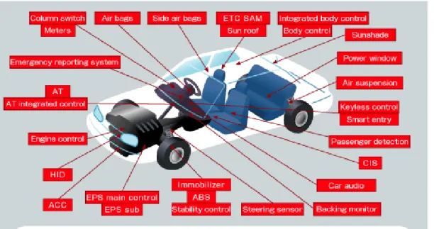
MCU with embedded memory already have more than 20 years history. At the beginning, only low density EEPROMs were integrated into the chip with microprocessor. As the system getting more complicated, higher density and higher performance embedded Flash technologies are developed to meet the application. Especially for automotive application, as shown in Fig.1.2, the latest cars have microcomputers in from 30 to 200 different locations, performing a wide range of powertrain control, vehicle ride, handling control, safety, comfort and convenience functions. There are many players in this market and each one has each own technology. In the following, four important technologies are chosen for brief discussion.
1.2.1 1T Stack-gate Technologies
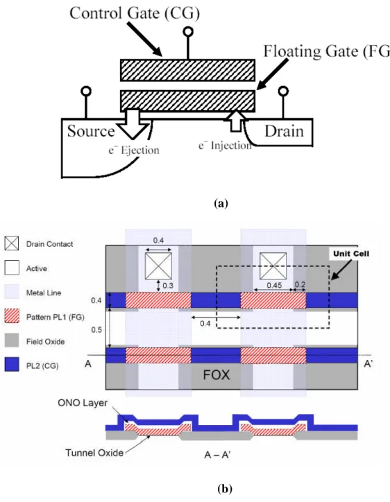
The 1T stack-gate NOR array has dominated the high-end embedded Flash application for automotive application for years because of the small cell size and longtime good reliability record. Products with this structure in present market are mainly based on the ETOX concept (EPROM with Thin Oxide), which was proposed by Intel in 1984 [3]. Fig.1.3 (a) and (b) show the schematic cross sectional view along the channel direction and the top view of an industry standard stack gate cell.
Programming is performed by channel hot electron injection occurred near the drain side with control gate voltage(VCG) of 9-11 V, drain voltage (VD) of 4-6V, typically, in several µs. Erase is achieved by Folwer-Nordheim (FN) tunneling from FG to source or to both source and channel regions in a range of ms to several seconds. The threshold voltage(VT) distribution of the Flash array after programming,
electrical erase and UV erasure is shown in Fig.1.4 (a) [4]. One of the major problems of this cell is the wide VT distribution after electrical erase. If the VT is too low to turn off the unselected cell completely, a high bit line current will occur and cause read failure as shown in Fig. 1.4 (b). Different models have been presented with the aim to explain the tail cells. For example, a distribution in the polycrystalline structure of the FG, with a barrier height variation at the grain boundaries, would give rise to a local enhancement of the tunnel barrier.[5]. Another model explains the tail cells as due to randomly distributed positive charge in the tunnel oxide [6]. To overcome the wide VT distribution after erase, a complicated erase and program algorithm is required. The algorithm includes the program/erase verification and a soft programming mechanism to tighten the VT distribution after erase. The graphical illustration of this operation is shown in Fig.1.5. This kind of algorithm will require a sophisticated state machine. For the high density embedded Flash application like engine control, the large overhead circuit might not be a concern because the penalty can be compensated by the small cell size [7]. However, for the commercial MCU application, the Flash density is typically smaller than 1-2Mb as shown in Fig.1.b, the large overhead circuit for program and erase control is not practical. In addition, the conventional channel hot electron programming is not efficient, it would require high current during data writing, which is not favored by the low power application. As a result, several technologies immune from over-erase issue are developed for the embedded Flash application; such as, split gate, 2T stack gate and fully overlap stack gate technology. We will briefly introduce these technologies in the following.
SuperFlash [8][9]. The advantage of this structure are low power consumption, fast access times and the immunity to over-erase issue. Generally speaking, split-gate structure uses source-side channel hot electron injection for programming, which has much higher program efficiency than drain side channel hot electron injection, and the erase is accomplished by field enhanced FN erase [10]. In Fig.1.6, due to the presence of the control gate (wordline), there is no concern for over-erase issue. Even though the unit cell size is larger than 1T stack gate, the chip area for small density array; like 1-2 Mb, is actually smaller than 1T stack gate cell because there is no extra circuit to control the VTdistribution.
The split gate structure can be used not only floating gate but also on local trap technology. As shown in the Fig.1.7(a) & (b) published by Freescale and Renesas, the advantage of split –gate technology is well recognized in the MCU application [11][12].
1.2.3 2T Stack-gate Technology
The cell consists of a select transistor(Tr) and a memory transistor(Tr) as shown in Fig. 1.8(a). Both select and memory transistor have the gate structure with the same with gate oxide, and the same symmetrical source/drain structure [12]. The memory array structure is shown in Fig.1.8(b).
The schematic operation diagrams are shown in Fig.1.9. In program mode, the VCG is applied with 12V and drain voltage is grounded on the selected cell , so the electron can be injected from channel to FG through FN tunneling. For unselected cell, the inhibit drain voltage is directly applied at the drain of memory Tr., and this inhibit drain voltage is cut-off by select Tr. In the erase mode, the erase voltage is divided into negative voltage and positive voltage, and Vcc is applied at a gate of select-Tr to reduce an electric field in the thin gate oxide of select-Tr. These approaches realize
channel FN program & erase and offer a high performance select-Tr with the thin gate oxide at the source side of memory cell. The advantages of this technology are low program and erase current, immune from over-erase issue, word re-writable and scalable to more advanced node. This cell is good for smart card application but the Flash macro size is still bigger than the split-gate Flash approach because of the 2T nature. Another drawback is slow program which is caused by FN tunneling.
1.2.4 Fully overlap Stack-gate Cell
Drawing of top view and cross-section views of the cell are shown in Fig.1.10. Theactiveregion,which hasaheavy outline,hastheform oftheletter“Z” in thetop view [13]. A first layer of polysilicon is used to form a floating gate memory transistor. A second layer of polysilicon, called the control gate, cover the floating gate and extends beyond the floating gat eon all sides. This second layer of poly forms a select transistor on each side of the floating gate. The coupling between FG and control gate is enhanced due to the fully overlap structure.
The programming is accomplished by applying a high positive voltage ~12-13V to the control gate of a cell in a grounded n-well causes electrons to tunnel from the accumulated well to floating gate. The cell is erased by biasing the n-well and bit line at a high positive voltage, typically 14-15V, and grounding the control gate. The operation condition is illustrated in Fig. 1.11.
Since this cell use FN tunneling for program and erase, and has the select transistor function because of the extended gate structure, so it has the advantage of low write current, immunity from over-erase and word re-writable function. However, the misalignment of the extended gate structure limits the scalability toward smaller
1.3 Purpose of this work
The traditional embedded Flash technology using ETOX cell requires more than 10 masking steps and complex state machine to control the programmed and erased VT
distribution. The split-gate Flash technology can perform the robust programming and erase function without state machine, however, it still needs the same complex process as stacked-gate floating technology. Moreover, it faces more serious hurdle to scale the cell size. The content of this thesis is divided into two parts; one is split-gate technology and another one is the novel metal gate EEPROM. For split-gate technology, we developed a new characterization to analyze the optimal program condition in terms of programming and disturb window, and we successfully developed a new high source coupling split-gate Flash cell which can operation at lower voltage and be more scalable. For novel metal gate EEPROM Flash, a new Flash EEPROM process with logic process compatibility is successfully demonstrated. The operation voltage can even be lower down to 6.5V and the extra masking steps over logic can be reduced to below 3. This new cell is very suitable to embedded application. The organization of this thesis is described in the following:
Chapter 2 describes the programming and erasure model for split-gate flash. It layouts the foundation for the programming optimization and new device development.
Chapter 3 introduces a new characterization technique to find the optimal programming condition, which can have the maximum programming and disturb window. This technique has been successfully utilized in the development for 0.18 split-gate Flash technology and beyond.
Chapter 4 disclose a new split-gate Flash cell with high source coupling ratio. With this new cell, we can have more room to reduce the floating length and lower down the operation voltage. We demonstrated the manufacturability of the cell by showing that the wafer sort yield (before and after retention bake) of 32Mb product is the same as the traditional process.
Chapter 5 reveals a novel metal gate EEPROM cell, which requires only 3 extra masking steps over standard logic process. The cell size is much smaller than conventional logic MTP cell. Because of the advantage of low extra masking steps, low voltage operation(<6.5V) and small cell size, this new technology is very suitable for embedded application.
(b)
Fig. 1.1 (a)Estimate from 2004 to 2010 for unit shipments of flash MCU chips. (b) Flash MCU characteristics and memory density by application type [2].
(a)
Fig. 1.2 Rapid increasing numbers of microcomputers are used in vehicles. The latest cars have microcomputers in from 30 to 100 different locations.
(a)
(b)
Fig. 1.3 (a) Schematic cross sectional view of stacked gate Flash memory cell along cell channel direction. The programming is through hot electron on drain side and erase is accomplished by FN tunneling in source side. (b) Top view and cross sectional view along with direction of stacked gate Flash memory cells fabricated in 0.35-m technology.
Fig. 1.4 (a) Threshold voltage distribution of a 1-Mb Flash array after UV erasure, after CHE programming, and after FN erasure. (b) In NOR array architecture, the leaky bit can cause the read failure on selected bit line [4].
Whole bit line leaky due to leaky bit
Fig. 1.5 VT shift during erase algorithm. A soft program after bulk erase can
effectively tighten up the VTdistribution.
0 1 2 3 4 5 6 7 8 9 10
Fig. 1.6 Schematic illustration of triple self-aligned split-gate Flash cell (SuperFlash®) proposed by SST.
(a)
(b) (c)
Fig. 1.7 (a) Schematic of split gate nano-crystal bit cell for control gate-first and select gate-first integrations by Freescale. [11], (b) Cell structure of MONOS split gate flash memory by Renesas [12], (c) Technology roadmap of Embedded Flash MCU by Renesas [12].
(a)
(b)
(a)
(b)
Fig.1.11 (a) Circuit schematic drawing, (b) The operating conditions for word rewritable array
Reference
[1] P. Cappelletti, C. Golla, P. Olivo and E. Zanoni, Flash memory, Kluwer Academic Publishers, 2000, pp. 482
[2] “Non-Volatile Embedded Memories (Applications, Technologies, Users, IP Suppliers and Foundries),”Memory Strategies International, Sept. 2006, pp. 9-10. [3] G. Verma and N. Mielke, “Reliability performance of ETOX based Flash
memories,”Proc. IRPS, 1988, p.158.
[4] R.Bez,E.Camerlenghi,A.Modelli,A.Visconti,“Introduction to Flash Memory,” in Proceedings of the IEEE, Vol. 91, No.4, Apr. 2003, pp. 489-502.
[5] S. Maramatsu, T. Kubota, N. Nishio, H. Shirai, M. Matsuo, N. Kodama, M. Horikawa, S. Saito, K. Arai, and T. Okazawa, “ The solution of over-erase problem controlling Poly-Si grain size –Modified scaling principles for Flash memory,”in IEDM Tech. Dig., 1994, pp.847-850
[6] C. Dunn, C. Kay, T. Lewis, T. Strauss, J. Screck, P. Hefley, M. Middendorf, and T. San,“Flash EEPROM disturb mechanism,”in Proc. Int. Rel. Phys. Symp., 1994,
pp. 299-308
[7] C.Deml,M.Jankowski,C.Thalmaier,“A 0.13µm 2.125MB 23.5nsEmbedded Flash with 2GB/s Read Throughput for Automotive Microcontrollers,”
International Solid-State Circuits Conference, 2007, pp. 478.
[8] S. Kianian, A. Levi, D. Lee, and Y.W. Hu, “A novel3 volts-only, small sector erase, high density Flash E2PROM,”in Symp. VLSI Technology Tech. Digest, 1994,
pp. 71-72.
[9] V.Markov,X.Liu,A.Kotov,A.Levi,T.N.Dang,and Y.Tkachev,“SuperFlash memory program/eraseendurance,”in Proc. NVM Tech. Symp., 2003.
Maes,“HIMOS –A high effiencency Flash E2
PROM cell for embedded memory application,”IEEE Trans. Elect. Dev., vol.40, pp.2255-2263, Dec, 1993.
[11] J.A. Yater, S.T. Kang, R. Steimle, C.M. Hing, B. Winstead, M. Herrick, G. Chindalore, “Optimization of 90nm Split Gate Nanocrystal Non-Volatile Memory,”NVSMW 2007,pp.77-78
[12] M.Hatanaka,T.Toya,“Applying Advanced Technology and Building a Stronger Product Rang to Make OurFlash&FlexibleMicrocomputerSuperiorSolutions”, [online]. Available: http://resource.renesas.com/lib/eng/edge/11/special03.html [13] J. Caywood, C.J. Huang, Y.J. Chang,”A NivelnonvolatileMemory CellSuitable
for Both Flash and Byte-Writable Applications,”IEEE Trans. Electron Devices, Vol. 49, no.5, May 2002, pp. 802-807.
Chapter 2
Split-Gate Flash Operation
2.1 Introduction
The split-gate Flash cell in this thesis is built on 2nd generation of SuperFlash technology from Silicon Storage Technology, Inc.(SST)[1][2]. It use triple self-aligned technology to reduce cell size and improve coupling ration [3][4]. The superFlash technology and memory cell have a number of important advantages for designing and manufacturing flash EERPOM, or embedding the memory in logic devices, when compared with the thin oxide stacked gate or two transitor approaches. The split-gate memory cell is comparable in size to the single transistor stacked gate cell, yet provide the performance and reliability benefits of the traditional two transistor byte alterable EEPROM cell. By design, the split-gate memory celleliminatesthestacked gateissueif“overerase”,by isolating each memory cell from thebitline.“Erasedisturb”can notoccurbecauseallbytesaresimultaneously erased in the same sector and each sector is completely isolated from every other sector during high voltage operation.
2.2 Cell cross-section and Layout
A top view and a cross –sectional view along bit line are presented in Fig 2.1. Polysilicon with silicide is used to connect control gate along the word line (row). Metal is used to connect the drain of each memory cell along the bit line (column). A common source is used for each sector, i.e., each pair sharing a common source along a row pair. A single word line is referred to as a row; the combination of pairs of rows form a sector, which is erased as a entity. Programming is done by word-by-word.
Fig.2.2 (a) is an equivalent memory cell, showing how the split-gate cell function as a select transistor and a memory transistor [5]. The memory array schematic is presented in Fig.2.2(b) , showing the logic organization of the memory array. This illustration represent a section of a typical cross-point memory array, arranged as 8 memory cells in 2 columns (bit lines), 2 sources lines, and 4 word lines. The cell operation condition is shown in Fig. 2.3. During the Read operation, reference voltage(2.5V) is applied to the control gate and the selectgatevia theword line.Thereferencevoltagewill“turn on”theselectgateportion of the channel. If the floating gate is programmed (high threshold state), the memory transistor portion of the channel will not conduct. If the floating gate is erased (negative threshold state), this memory cell will conduct. The conducting state is output as a logic ‘1”, the non-conducting stateisalogic“0”.
2.4 Programming
The cell programs using high efficient source-side channel hot electron injection. During programming, a voltage higher than the threshold (Vt) of the select transistor is placed on the control gate via the word line. This is sufficient to turn on the channel under the select portion of the control gate. The drain is biased at low voltage (~0.5) under a constant current circuitry if the cell is to be programmed. If the drain is at Vdd, programming is inhibited .The drain voltage is transferred across the select channel because of the voltage on the control gate. The source is bias at high voltage around 7~9V. Generally speaking, the source to drain voltage differential generate channel hot electrons. The source voltage is capacitively coupled to the floating gate. The field between the floating gate and the channel very efficiently sweeps the hot electrons across the Si-SiO2 barrier (~3.2eV) to the floating gate. To understand the programming mechanism in more detail, we can divide the programming operation into three regions [6]. The graphical illustration is shown in Fig. 2.4.
1) Region-A: VFG> VSS+ VTFG: (SG in saturation and FG in linear)
Where SG is the select gate transistor, FG is the floating gate transistor, VSS is the
potential at source node, VFGis the FG potential, VTFGis the threshold voltage of the FG.
The region happens when the cell is under deeply erased that the floating gate voltage is higher than the Vss voltage plus its threshold voltage. In region-A, the virtual drain extension concept [7] is valid and the channel surface potential at the gap is approximated as the drain potential. When VSGis chosen much smaller than VSS, a hyperbolic cosine-shaped lateral field
[8] will be built up at the SG saturation region as shown in Fig. 2.4(a) and accelerates source-side injected electrons to jump into the FG.
2) Region-B: VSG_SAT+ VTFG≤VFG≤VSS+ VTFG(SG in saturation, FG in saturation)
Where VSG_SATis the saturation voltage of select transistor.
Most of the hot electron injection occurs in this region. FG transistor acts as a source follower, which can pass high voltage around VFG-VTFG. Since SG is slightly turn-on, this
high voltage (VFG-VTFG) will make SG transistor operate in saturation region. This saturation
region near SG/FG gap can generate high lateral electric field and trigger hot electron injection. The voltage drop between the pinch-off points of FG and SG is shown in Fig.2.5 (a), and the pinch-off potentials for FG at point A and for SG at B are expressed as:
TFG FG A V V V (1) TSG SG B V V V , (2)
where V is the potential at point A,A V is the potential at point B,B VFG is the FG potential,
TFG
V is the threshold voltage of the FG,VSG is the SG potential, and VTSG is the threshold
voltage of the SG.
In the split-gate flash program operation, a significant voltage drop in the longitudinal direction occurs between A and B; thus, the injection point is moved from the conventional
“source-side”or “mid gate”hot carrier injection. From eqs. (1) and (2), the average longitudinal electric field ( EX ) in the poly gap (A-B) region can be express as [9]-[11].
) /( ) ( A B A B X V V X X E . (3)
For first-order approximation, we can let VTFG be equal to VTSG and (XA XB) to k ,LG
where L is the spacing between FG and SG, andG k is the fitting parameter [9]. Thus, eq. (3)
can be simplified to G SG FG X V V k L E ( )/ . (4)
For a vertical oxide electric field at the injection point, the field is approximately
OX C FG
OX V V T
E ( )/ , (5)
VCwill fall between VAand VB.
Assuming the storage charge in the floating gate is zero, the floating gate voltage (VFG) is
mainly coupled from FG and SG. It can be expressed in the following equation:
SS S SG G SS S T FG FG Q C V V V V / , (6)
where QFGis the floating gate charge, CTis the total capacitance, is the Vss coupling ratioS
on FG (SCR), and is the select-gate coupling ratio on FG.G
Insert eq. (6) into (4) and (5), we can further derive the EX and EOX ‘srelation with andS VSS. G SG SS X V V k L E ( )/ (7) OX C SS OX V V T E ( )/ (8)
With split –gate structure, we can achieve highEX and a highEOX favorable for electron
injection at the same location. On the basis of the lucky-electron model (LEM), the injection current is determined by [12]-[13],
EX
Exp E Is K
n
X
b b FG-2 I , (9)
where IS is the programming current, is the scattering mean free path, and b is the
effective barrier height and commonly expressed as
2/3 1/2 OX OX E E
θ
β
b
b0 . (10)Here, b0 is the zero-oxide-field potential barrier (b0 = 3.1 V), the second term is the
Schottky barrier-lowering effect due to the image field, and the last term is the tunneling-related barrier-lowering coefficient [14].
From eqs. (9) to (10), we note that an increase in EX and EOX can significantly improve
program efficiency because channel electrons can gain more kinetic energy along longitudinal direction and have lower barrier height for injection to floating. The simulation result is shown in Fig.2.5 (b). A high electron injection probability occurs when high EX and EOX are
aligned in the FG/SG gap region, as a result the hot electron injection efficiency in split-gate cell is 1000 times more than the stack-gate counter part.
3) Region-C, VFG≤ VSG_SAT+ VTFG(SG in linear, FG is saturation)
In this region, VFG is so low that the voltage passed through FG transistor cannot cause
the SG transistor to be in saturation mode. The function of SSI programming will cease because source side injected electrons gain no more energy at the gap.
2.5 Field Enhanced Fowler-Nordheim Tunneling
The cell erases uses Fowler-Nordheim tunneling from the floating gate to the control gate. During erasing, the source and drain are grounded and the word line is raised to a high voltage. The low coupling ratio between the control gate and the floating gate provide a significant voltage drop across the inter-poly oxide. A local high electric field is generated primarily along the edge of the tunneling injector. Charge transfer is very rapid (~1ms) and is
sustain Flower-Nordhein tunneling. The graphical illustration of field enhanced poly-to-poly FN tunneling is shown in Fig.2.6. A sharp tunneling injector is formed by special slop etching on FG in the triple self-aligned split gate flash technology. Unlike the traditional erasure by the Fowler-Nordheim tunneling though a triangular barrier, which requires a higher voltage across thin tunneling oxide. The field enhanced tunneling through sharp tip can be achieved at lower voltage and with thicker oxide to maintain good data retention performance. Using a cylindrical approximation, the electric field is highest ( EMAX ) at the inner edge and lowest ( EMIN ) at the outer edge [15];
a T a
V
EMAX OX / ln1OX / , (11)
where a is the radius of curvature of the smaller cylinder, and
FG SG OX V V
V . (12)
The tunneling current is described by the Fowler-Nordheim tunneling equation.
Ifg=AEOX2e-B/Eox (13)
Where A and B depends on the material property of the oxide and interface.
2.6 Summary
An analytical programming and erasing model is introduced in this chapter. It layouts the physical foundation for the following chapters on program/disturb window study and the new split-gate Flash cell design.
(a)
(b)
Fig.2.1 (a) Cross-section of triple self-aligned split-gate Flash cell in bit-line direction, (b)
Word Line
Word Line
Source Line
Floating
Gate
Drain
"Program" S ource
Drain
"Erase"
(Control Gate)
(Control Gate)
(a)
(b) Fig.2.2 (a) Equivalent circuit of split-gate Flash cell, (b) Cell array schematic
1. Faster programming (100X) efficiency by “source-side injection”.
2. Better erase efficiency by “field-enhanced”FN tunneling.
3. No over-erase concerns because of select-gate structure.
4. One shot PGM and ERA, no verification CKT is needed.
1. less over-head CKT smaller die size.
2. Easier design good for embedded application.
Vwl Vbl Vss Vsb
PGM 1.8 Vdp 7~9V 0
ERA 12~13V 0 0 0
Fig.2.4 Simulation results of the lateral field distribution along channel surface for (a)
region-A (b) region-B (c) region-C. The enlarged schematic cross-section with electron flow lines
during programming is shown in (b). In the inset of (b), point A (or A’) marks the physical boundary between SG (or FG) and IPO. Point G (or G’) marks the position of the maximum lateral field. The device parameters are: LSG= 0.3m, LFG= 0.183m, LFG= 0.4m, TSGOX
= 180 Å, TFGOX = 100 Å [6]
(a)
Programming
Ey
Region A
FG:Linear
SG:Sat.
-NN +
S
(b)
e
-e
-Ey
L
gapA'
A
G'
G
L
FGL
FGL
SGD
D'
G'
G
P'
P
Lines FlowFG:Sat.
D
S
SG
SG:Sat.
FG
Ey
Region B
(c)
Ey
Region C
FG:Sat.
SG:Linear
Fig.2.5 (a) Pinch-off point of FG and SG is A and B, respectively. Electron injection point is C, where is located in floating gate edge on the poly space. (b) Electric field and electron injection probability distribution.
0 200000 400000 600000 800000 1000000 0 0.1 0.2 0.3 0.4 0.5 0.6 X-coord E x ,E y (V /c m ) 0 200 400 600 800 1000 1200 E le c tr o n _ In je c t_ P ro b EX EY Pinj(e-) Bit-line Word-line Vss Contact (sectect gate)
Floating gate Drain Source
(a)
B C A(select gate)
(a)
(b)
LG Floating gate 0 200000 400000 600000 800000 1000000 0 0.1 0.2 0.3 0.4 0.5 0.6 X-coord E x ,E y (V /c m ) 0 200 400 600 800 1000 1200 E le c tr o n _ In je c t_ P ro b EX EY Pinj(e-) 0 200000 400000 600000 800000 1000000 0 0.1 0.2 0.3 0.4 0.5 0.6 X-coord E x ,E y (V /c m ) 0 200 400 600 800 1000 1200 E le c tr o n _ In je c t_ P ro b EX EY Pinj(e-) Bit-line Word-line Vss Contact (sectect gate)Floating gate Drain Source
(a)
B C A(select gate)
(a)
(b)
LG Floating gateFig.2.6 (a) Magnification of poly tip for tunneling, (b) energy band diagram during erasing, Emax is near the poly tip due to field-enhanced effect.
.
a
Tox
a
T
a
V
E
MAX
OX/
ln
1
OX/
Floating gate oxide select gate
Vox
(a)
(b)
a
Tox
a
T
a
V
E
MAX
OX/
ln
1
OX/
Floating gate oxide select gate
Vox
(a)
Reference
[1] S. Kianian, A. Levi, D. Lee, and Y.-W. Hu, “A novel 3 volts-only, small sector erase, high density Flash E2PROM,”in Symp. VLSI Technol. Dig., 1994, p. 71-72.
[2] B. Yeh, “Single transistor non-volatile electrically alterable semiconductor memory device,”United States Patent 5,029,130, 1991.
[3] W.T. Chu, H.H. Lin, C.T.Hsieh, H.C. Sung, Y.H. Wang, Y.T. Lin, C.S. Wang, “ShrinkableTripleSelf-Aligned Field-Enhanced Split-GateFlash Memory,” IEEE Trans.
Electron Devices, vol. 51 no. 10, pp. 1667-1671, 2004
[4] R. Mih, J.Harrington, K. Houlihan, H.K. Lee, K. Chan, J. Johnson, B. Chen, J. Yan, A. Schmidt, C. Gruensfelder, K. Kim, D. Shum, C. Lo, D. Lee, A. Levi, and C. Lam, “0.18um Modular Triple Self-Aligned Embedded Split-Gate Flash Memory,”in Symp.
VLSI Technol. Dig., 2000, pp. 120-121.
[5] “SuperFlash EEPROM Technology,”SST Technical Paper, November, 2001
[6] Y.H.Wang, M.C. Wu, C.J. Lin, W.T.Chu, Y.T. Lin, C.S. Wang, K.Y. Cheng, “An Analytical Programming Model for the Drain-Coupling Source-side Injection Split Gate Flash EEPROM,”IEEE Trans. Electron Devices, vol. 52, no. 3, Mar 2005, pp. 385-391
[7] H.S.Wang,“Gatecurrentinjection in MOSFET’swith asplit-gate (virtual drain) structure “IEEE ELECTRON DevicesLett.,vol.EDL-14, pp.262-264, May 1993
[8] P.K.Ko,“Hot-electron effectin MOSFET”Ph.D.dissertation,Univ.California,Berkeley, 1982
[9] H. Guan, D. Lee and G. P. Li,“An analytical model for optimization of programming efficiency and uniformity of split gate source-side injection superflash memory”IEEE
[10] ] J. V. Houdt, G. Groeseneken and H. E. Maes, “An analytical model forthe optimization of source-side injection flash EEPROM devices” IEEE Trans. Electron
Devices, vol. 42, pp. 1314–1320, July 1995
[11] J. V. Houdt, P. Heremans, L. Deferm, G.Groeseneken and H.E.Maes,“Analysis of the Enhanced Hot-Electron Injection in Split-Gate Transistors Useful for EEPROM Applications”IEEE Trans. Electron Devices, vol. 39, pp. 1150–1156, May 1992
[12] C. Hu, S. Tam, F.C. Hsu,P.K.Ko,T.Y.Chan and K.W.Terill,“Hot-electron-induced MOSFET degradation – model, monitor and improvement,” IEEE Trans. Electron Devices, vol. ED-32, Feb. 1985, pp.375-384
[13] S. Tam, P. K. Ko and C. Hu,“Lucky-electron model of channel hot-electron injection in MOSFET’s”IEEE Trans. Electron Devices, vol. 31, pp. 1116–1125, Sep. 1984.
[14] ]T.H.Ning,C.M.Osburn,and H.N.Yu,“Emission probability ofhotelectrons from silicon into silicon dioxides”J. Appl. Phys., vol. 48, pp. 286–293, Jan. 1977.
[15] A. Kotov, A. Levi, Yu. Tkachev, and V. Markov, “Tunneling phenomenon in superflash cell”Proc. NVM Tech. Symp., 2002. pp. 110-115
Chapter 3
Novel Program vs Disturb Window Characterization
for Split-Gate Flash Cell
3.1 Introduction
In this chapter, a new methodology for program vs. disturb window characterization on split gate flash cell is presented. The window can be graphically illustrated in VWL
(word-line)-VSS (source) domain under a given program current. This method can let us
understand quantitatively how the window shifts vs. bias conditions and help us to find the optimal program condition. The condition obtained by this method can have the largest operation window in programming and disturb. This methodology has been successfully implemented in the development for 0.18um triple self-aligned (SA3) split-gate technology and beyond.
The split-gate flash memory proposed by Silicon Storage Technology Inc. (SST) is commonly used in stand-alone and embedded non-volatile memory because of the advantages of fast erase speed, high programming efficiency, and most important, no verification after program and erase. The erase is achieved by field-enhanced F-N tunneling through sharp poly tip, and the program is accomplished by source-side hot carrier injection (SSI) [1][2]. Although the above mechanisms provide good physics foundation for fast erase and program, a robust characterization methodology for determining operation condition is still crucial to guarantee reliable one shot program and erase. For erase condition, the window characterization is more straightforward because word-line voltage is the only parameter. Generally, higher word-line voltage yields faster erase speed and better cycling performance
voltage transistors. The optimization of erase voltage is typically determined by the trade-off between HV circuit reliability and endurance cycling. However, the program window characterization is much more difficult due to its complex bias conditions for both selected and un-selected cells. A good program condition requires not only fast program efficiency on selected cells but also very limited disturb effect on un-selected cells. The variables involved in the programming are programming current, word-line voltage and source-line voltage, and the figure of merit is the programming speed and three types of disturb behaviors. It is not a simple task to find an optimal condition among those variables. In this paper, we successfully develop a new methodology for program vs. disturb window characterization. This method can convert the constraints on programming and disturb into a clear graphical illustration. We can quantify the programming window from the 2D graph and use the data to find the optimal program condition from single cell measurement.
3.2 Experiment
The flash memory cells used in this study were fabricated by 0.18 m triple self-aligned (SA3) Split-gate Flash technology [4]. The graphical illustration of process flow is shown in in Fig.3.1 [4][5]. Firstly, floating gate oxide is grown prior to floating gate poly deposition. Next, shallow-trench isolation (STI) is formed to become the 1st self-alignment to floating gate. After memory well implantation and thick nitride deposition, the region for floating gate and source line is defined and opened. Then, thick TEOS spacers and source poly lines are formed to become the 2nd self-alignment, which is source-line to floating gate. After thick nitride is removed, floating gate is defined by TEOS hard mask, and HTO is deposited to act as tunneling oxide. Afterwards, word-line poly was deposited and etched to become spacer word-line, which is the 3rd self-alignment to floating gate. After this step, the Flash cell is finished. The standard logic process flow for source & drain implant and metallization will be
followed. The cross-sectional view of SEM and TEM pictures of the cell are shown in Fig. 3.2 [4].
3.3 Program vs. Disturb Window Characterization
As shown in Fig.3.3, the memory cells are arranged in a cross point array, using a word line and bit line for address location selection; thus, unselected cells within same page will suffer the stress from high VSSvoltage, and this is where the program disturb comes from.
There are three types of possible program disturbs, and they will be described in the following paragraph. The cells in different page will not have program disturb because each sector is individually isolated. Each cell is only exposed to higher voltage within the selected page along row or source line; there is no high voltage on the bit line.
In triple self-aligned split-gate Flash, programming is operated at following conditions: Source node (VSS) biased at high voltage, word-line (VWL) slightly turned-on and bit-line
connected to a constant current source (Idp). This program condition can cause three disturb stress modes; they are: Column Punch-through Disturb (PTC), Row Punch-through Disturb (PTR) and Reverse Tunneling disturb (RT) [6][7]. The disturbed bits’location and stress conditions are shown in Fig.3.3. The program time and disturb duration are determined by product spec and array architecture. In this paper, we use 32Mbit Flash as a target vehicle. The program time is 10us, and the disturb time for PTC, PTR and RT is 1ms, 40ms and 260ms, respectively. For the criteria in this characterization, the program spec is defined as “programmed state current (Ir0) smaller than 5% of erased state current (Ir1)”, and the disturb spec is defined as “cell current drop ratio (ΔIr1/Ir1) smaller than 10% after program disturb”. For a given program current (Idp) and program time, the program vs. disturb window can be presented in the VWL (word-line)-VSS (source) domain. The plot is shown in Fig.3.4. A
shown below. Note that the VSSvoltage is constrained at 9V to prevent device form damage.
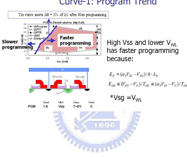
Curve 1: Programming.
The curve meets Ir0 = 5% of Ir1 after 10us programming. As shown in Fig.3.5, the lower right side of curve 1 (higher VSS and lower VWL) is the region satisfying program specifications.
Based on the eqs. (7) & (8) shown in Chap.2, we can find that a higher lateral and vertical field can be induced by higher VSS and lower VSG(=VWL), as a result, the programming is
better in this region.
G SG SS X V V k L E ( )/ OX C SS OX V V T E ( )/
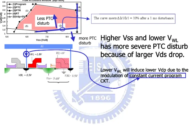
Curve 2: Column punch-through (PTC) disturb.
The curve meetsΔIr1/Ir1 = 10% after a 1 ms disturbance. The upper left side of the curve 2 (lower VSS and higher VWL) is the region satisfying the PTC disturbance specifications. The
bias condition and the disturb trend is shown in Fig.3.6. The source and bit lines of PTC are the same as those of programming-selected bits, while the word lines of PTC are grounded to turn current off. In a real situation, a small amount of leakage can still exist and cause undesired injection under a high source-to-drain voltage drop. The disturb will get worse when the source-to-drain voltage drop get higher. The higher VSS can cause larger VDS is
obvious. However, the effect of VWL on PTC is through the modulation of constant current
programming circuitry. To maintain constant current programming, Vdp will be lower when the VWLin selected cell becomes lower, and thus the source-to-drain voltage drop in PTC cell
get larger. Therefore, the region with higher VSS and lower VWL will have larger
source-to-drain voltage drop and will be easier to get PTC disturb. As shown in the illustration of the PTC disturb trend on the VSS-VWLdomain, the upper left side of the curve 2 (lower VSS
and higher VWL) is the region satisfying the PTC disturbance specifications.
Curve 3: Row punch-through (PTR) disturb
line of program-selected bits, so the word line is turned on and the source line is biased at a high voltage. The bias condition and the PTR trend is is shown at Fig.3.7. To prevent undesired programming on the erased cell, an inhibited voltage (~2 V at the worst case) is applied to unselected bit lines to stop the leakage flowing from the source to the drain. However, when the back bias is not strong enough to shut off the leakage, the undesired programming will occur. Thus, PTR tends to occur under higher VWLand VSSvoltages. As a
presentation of this trend on the VSS-VWLdomain, the bottom left side of curve 3 (lower VWL
and lower VSS) is the region satisfying the PTR disturbance specifications.
Curve 4: Reverse tunneling (RT) disturb
The curve meets ΔIr1/Ir1 = 10% after a 260ms disturbance. RT occurs on the bits at the condition that the source line is connected to a high voltage, word line is grounded and bit line is biased under an inhibited voltage. This is the most minor disturb mode in split-gate Flash. The bias condition and RT disturb trend is shown in Fig.3.8. The disturb mechanism is solely caused by reverse tunneling from the word line to the floating gate and is only dependent on VSS voltage. Higher the VSSvoltage, worse the reverse tunneling disturb. Therefore, the left
side of the curve is the region satisfying the RT disturbance specifications. This disturb mode can be totally eliminated if a good process is chosen to suppress FG undercut during floating gate etching. In this characterization, the VSS is clamped at 9V to prevent device from
damage.
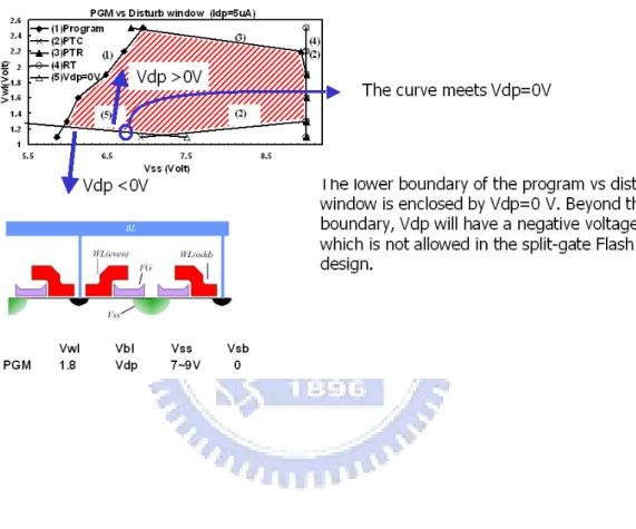
Curve 5: Drain voltage during programming (Vdp)=0V
The lower boundary of the program vs disturb window is enclosed by Vdp=0 V. Beyond this boundary, Vdp will have a negative voltage, which is not allowed in standard split-gate Flash design.
3.4.1 Finding optimal program condition
To find an optimal program condition from the program/disturb window characterization, a maximum circle, named as operation circle, is drawn within the enclosed window, as shown in Fig. 3.10. The circle center can be chosen as the best program condition for a given Idp. The reason is that the circle center has largest voltage variation allowance for VWL and VSS.
Note that the scale at X and Y axis is kept the same.
Next step is to find the best Idp setting. As shown in Fig.3.11 (a), we can see that the operation window changes with Idp. When Idp is lowered from 5μA to 1μA, the window shifts to the higher VSS because higher VSSis needed to compensate the programmability loss
caused by lower Idp. On the other hand, when Idp is increased from 5μA to 9μA, the window shifts toward lower VSS and high VWL (weaker programming region) because the
programmability is enhanced by the higher Idp. Comparing the maximum circle size between Idp=1, 5, and 9μA in Fig.3.9 (b), we can find that Idp=5μA has the largest circle size, which means 5μA is the best program current setting. Therefore, we choose the center of operation circle at Idp=5μA as the best program condition. The bias condition is: VSS=7.2V, VWL=1.8V
at Idp=5μA. This methodology was successfully implemented in 0.18um SA3 single cell characterization to determine program setting for 32Mbit-product.
3.4.2 Constant voltage vs. constant current programming
For ETOX stack gate Flash cell, constant voltage programming is commonly used [8], while for super Flash Flash technology the constant current method is chosen to improved the operation window. Using the characterization method developed in this thesis, we can compare the operation window difference between these two program schemes. The circuit diagram is shown in Fig.3.12. We check the overlap window for constant current programming with Idp varying from 1-9uA, and the one for constant voltage programming
with Vdp varying from 0 to 0.6V. As shown in Fig. 3.13, we can find the constant current programming has much larger window than the constant voltage method. In constant voltage programming, the PTC disturb is very serious when Vdp ~0V, and the programmability is poor in low VWL when Vdp is ~0.6V, so the overlap window is very small. Under constant current programming, Vdp will vary to supply the stable programming current and the back bias effect can suppress the punchthrough from happening.
2.5 Summary
A new methodology for program vs. disturb window characterization in split gate flash cell is presented in this paper for the first time. With this new methodology, the optimal program condition can be determined from single cell measurement. In addition, the quantitative window information can help us to evaluate the trade-off clearly between various program settings.
(b)
Fig.3.3 Cell array and bias voltage for program, erase, read-out and three disturb conditions, which are: A. Column punchthrough disturb(PTC), B. Row punchthrough disturb(PTR), C. Reverse tunneling disturb(RT). Note that the cells outside the selected page are immune from disturb stress. Page m+1 (no disturb) Page m C:PTR 1.8 2.0 7.2 0 0 7.2 Vdp 1.8 S:Selected 0 7.2 2.0 0 B:RT 0 7.2 Vdp 0 A:PTC Vsub Vss Vbl Vwl 0 7.2 2.0 1.8 C:PTR 0 7.2 Vdp 1.8 S:Selected 0 7.2 2.0 0 B:RT 0 7.2 Vdp 0 A:PTC Vsub Vss Vbl Vwl Program bias 0 0 0.8 2.5 Read 0 0 0 12 Erase Vsub Vss Vbl Vwl 0 0 0.8 2.5 Read 0 0 0 12 Erase Vsub Vss Vbl Vwl
Erase & Read bias
BLn-1 BLn* BLn+1 BLn+2 WLm0(0V) Vss(7.2V) WLm1(1.8V) 2.5V Vdp 2.5V 2.5V B A B B C S C C BLn-1 BLn* BLn+1 BLn+2 WLm0(0V) Vss(7.2V) WLm1(1.8V) 2.5V Vdp 2.5V 2.5V B A B B C S C C
Note: Vdp is the selected bit-line voltage at Idp=5uA, the voltage is around 0.5V.
Fig.3.4 Program vs disturb window and the operation window. The programming time is 10us and program current is 5μA
PGM vs Disturb window (Idp=5uA)
1 1.2 1.4 1.6 1.8 2 2.2 2.4 2.6 5.5 6.5 7.5 8.5 Vss (Volt) V w l( V o lt ) (1)Program (2)PTC (3)PTR (4)RT (5)Vdp=0V (1) (3) (5) (2) (4) (2) (2) (5)
Fig. 3.5 Program trend in PGM vs Disturb window


![Fig. 1.9 Schematic diagram of the operation of 2 Tr stack gate cell [12].](https://thumb-ap.123doks.com/thumbv2/9libinfo/8234377.171086/34.892.146.761.277.800/fig-schematic-diagram-operation-tr-stack-gate-cell.webp)
![Fig. 1.10. Top and cross-section drawing of the fully overlap cell [13]](https://thumb-ap.123doks.com/thumbv2/9libinfo/8234377.171086/35.892.149.737.302.778/fig-cross-section-drawing-fully-overlap-cell.webp)