國 立 交 通 大 學
光電工程研究所
碩 士 論 文
微杯電泳顯示器內帶電粒子之電動力學
Electrokinetics of Charged-Particles
in Microcup Electrophoretic Displays
研 究 生:吳思頤
指導教授:黃乙白 博士
微杯電泳顯示器內帶電粒子之電動力學
Electrokinetics of Charged-Particles
in Microcup Electrophoretic Displays
研究生:吳思頤 Student:Szu-I Wu
指導教授:黃乙白 Advisor:Yi-Pai Huang
國立交通大學
光電工程研究所
碩士論文
A ThesisSubmitted to Institute of Electro-Optical Engineering College of Electrical and Computer Engineering
National Chiao Tung University in partial Fulfillment of the Requirements
for the Degree of Master
in
Electro-Optical Engineering
June 2011
Hsinchu, Taiwan, Republic of China
i
微杯電泳顯示器內帶電粒子之電動力學
碩士研究生:吳思頤 指導教授:黃乙白副教授
國立交通大學 光電工程研究所
摘 要
近幾年來,平面顯示器技術越趨成熟,在節能與環保的考量下,電子紙漸露光芒。 電子紙同時擁有一般顯示器資訊取得的便利性與及時性又有紙張的廣視角與攜帶的輕 便性。其主要可分為三類:穿透式顯示器,自發式顯示器與反射式顯示器。相對於液晶 顯示器,反射式電子紙較適合在戶外與長時間使用,且其雙穩態的特性使其更為節能, 所以目前市場上較為普遍的技術為反射式的電子紙顯示技術。目前應用於電子書、價錢 商標、軟性顯示器、智慧卡與手錶等。然而,反射式電子紙目前還有以下幾點需克服的 議題:(一)如何增快反應時間,使其可應於動態影片。(二)如何讓它色彩化。 隨著大眾越趨重視電泳式顯示器,更多研究開始投入這塊領域。但大部分偏向研究 量產方式、雙穩態品質、影像品質,少部分是研究內部電荷行為,導致目前物理機制的 研究不夠完備與統整。除此之外,幾乎沒有研究是特別針對微杯電泳式顯示器或是提出 此結構之模型來描述會影響電泳式顯示器的效能之內部帶電粒子行為。 本篇論文,除了反射式電子紙之電泳顯示器基礎物理特性之探討外,還結合電流與 光訊號來深入了解電泳顯示器內帶電粒子的運動機制,並利用其物理特性找出增快反應 時間的方法與設計出縮短驅動時間的波型。ii
Electrokinetics of Charged-Particles
in Microcup Electrophoretic Displays
Student: Szu-I Wu Advisor: Dr. Yi-Pai Huang
Department of Photonics & Institute of Electro-Optical Engineering,
Display Institute
National Chiao Tung University
Abstract
In recent years, the development of flat panel displays has been more mature. Under the consideration of power saving and environmental protection, E-paper starts to glow. E-paper possesses both the advantages from general displays and paper. It provides the convenience and instantaneousness of obtaining information as computer does but with lighter, thinner volume and wide viewing angle as paper is. E-paper can be classified into three types, the transmissive, emissive and reflective types. In comparison with the transmissive and emissive types, the reflective types are more power saving because of its bistability characteristics, which make them more commonly used in the market. This technology has been applied in E-books, price tags, flexible displays, smartcards and watches. However, there are still some issues require to be solved. First of all, the method of reducing transition time in order to put videos into practice. Second, the method for realizing color E-papers.
With a large interest in EPDs, research has been conducted mostly from manufacture type, image stability and the image quality. Fewer have been done from the internal charge behavior therefore findings regarding physical mechanism are not complete and unified. Besides, there was scarce research focus on Microcup EPDs or a model proposed to describe the motion of charged species which would be the major factor that dominates the criteria of EPD performances.
iii
electrophoretic type of E-papers but also combines current and optical responses to get deeper insight into electrokinetics of charged particles inside EPDs. Besides, some methods are proposed and verified to reduce the transition time and shortened driving waveforms are designed based on the discovered physical mechanisms.
iv
Acknowledgements
首先,要誠摯的感謝實驗室兩位老師,謝漢萍教授和指導老師黃乙白副教授在碩士 兩年的求學生涯中提供豐富的實驗室資源和良好的研究環境。對於研究過程、研討會報 告與英文能力的指導鞭策,培養我進入社會後所應具備的基本條件。也由衷感謝各位口 試委員對於本論文所提供的寶貴建議,使整體內容更加趨於完備。 另外,也特別感謝楊磊明博士後研究員在碩士第一年生涯的指導與參加國外研討會 時論文語文部分的修改。此外,更感謝林芳正博士後研究員,在碩士第二年生涯的指導 與帶領,無論是對於論文研究方向上的建議、在研究過程中遇到問題時的指導與幫忙、 研討會報告與論文的修改,還有精神上的鼓勵與打氣等,同時身為FSC與電子紙組別的 支柱實在是非常辛苦。學長除了具備超群的文書處理能力、表達能力,對於研究的熱誠 與專業是讓我最佩服之處,也成為我的學習榜樣。除此之外也謝謝同組的學弟一笑、楊 上翰在研究上的合作與幫忙,與你們一起實驗與問題討論是很振奮人心的事情。也謝謝 合作計畫公司的同仁楊柏儒、張明仁、黃若城學長,對於研究與實驗方向上面的建議、 協助與配合,使得一切能夠順利流暢的進行。 感謝實驗室台翔、精益、國振、凌堯、柏全、奕智、小皮、大頭、致維哥、與志明 等博班學長姐,提供各方面專業的指導與意見。也特別感謝上一屆學長姐小胖、玉米、 MOSS、筱儒、阿扁、謝小白等人,在我碩一時的照顧、呵護與陪伴。此外也謝謝碩二的 同學小馬、小頭、立偉、馬志堯、董哥、蓋B、昌毅、小發特、博六、子寬和江濟宇, 在這兩年中無論是在研究、課業和生活上一起打拼與互相扶持,讓實驗室增添許多趣味。 尤其是小馬、小頭與小皮學姐還有拉拉與張綺兩位學妹,同樣身為實驗室女生,有你們 在真好!另外,也要向實驗室的雅惠、穎佳、茉莉和江介堯四位助理們還有學弟妹們表 達最誠摯的感謝,讓我們在研究之餘無後顧之憂,並使實驗室整體像一個大家庭一樣隨 時充滿歡愉的氣氛。最後,對於我的家人及朋友們,感謝你們這兩年來背後的關懷、鼓 勵與陪伴,使我能夠無後顧之憂且順利地完成兩年的碩士學位,這份感激與喜悅要分享 給所有認識和幫助過我的人。v
Table of Contents
Abstract (Chinese)………...i.
Abstract (English)………...ii.
Acknowledgements………..iv.
Figure Captions ... vii
Chapter 1 ... 1
1.1 Classification of E-papers ... 2
1.2 Prior Arts of Electrophoretic Displays (EPDs) ... 4
1.2.1 Microcapsule EPD ... 5
1.2.2 Quick Response Liquid Powder Display (QRLPD) ... 5
1.2.3 Microcup EPD ... 6
1.3 Motivation and Objectives ... 7
1.4 Thesis Organization ... 8
Chapter 2 ... 9
2.1 Mechanism of Charged Particles ... 9
2.2 The bistability Mechanism ... 10
2.2.1 Colloid Behavior ... 10
2.2.2 The Electric Double Layer and Zeta Potential ... 11
2.2.3 Amplitude of Multiple Forces ... 14
2.3 Optical Characteristics ... 16
2.3.1 Wake-up time (WUT) ... 16
2.3.2 The paging time ... 17
2.3.3 The criteria of EPD performances ... 18
2.4 Summary ... 21
Chapter 3 ... 22
3.1 Experimental Setup and Instruments ... 22
vi
3.1.2 Driving box ... 23
3.1.3 Photo-diode ... 25
3.1.4 Current meter_ Keithley ... 26
3.1.5 Colorimeter_i1 ... 27
Chapter 4 ... 28
4.1 Three current states ... 28
4.2 Current Bump with Various Pulse Widths ... 30
4.3 Current Bump with Symmetric Waveforms ... 33
4.4 Symmetric Waveforms with an In-between Inserted duration ... 35
4.5 Application... 38
4.6 Summary ... 42
Chapter 5 ... 43
5.1 Conclusion ... 43
5.1.1 Model establishment ... 44
5.1.2 Pulse Width Modulation ... 44
5.1.3 Current Bump with Symmetric Waveforms ... 45
5.1.4 Application ... 46
5.2 Remaining Issues and Future Work ... 47
vii
Figure Captions
FIG.1-1E-PAPER PRODUCTS (A)E-BOOKS.(B)FLEXIBLE DISPLAYS.(C)PRICE TAGS.
(D)SMART CARDS. ... 1
FIG.1-2E-PAPER CLASSIFICATION. ... 2
FIG.1-3THREE STATES OF CHOLESTERIC LIQUID CRYSTAL DISPLAY [2]... 4
FIG.1-4AMICROCAPSULE EPD STRUCTURE [5]. ... 5
FIG.1-5AQRLPD STRUCTURE [6]. ... 6
FIG.1-6AMICROCUP EPD STRUCTURE [7]. ... 6
FIG.1-7CONFIGURATION OF A MICROCUP EPD. ... 7
FIG.2-1FORMATION OF (A) SURFACTANT DISSOCIATION (B) MICELLE, AND (C) PARTICLE CONFIGURATION INSIDE THE MICROCUP EPD[15][16]. ... 10
FIG.2-2SCHEME OF THE ION DISTRIBUTION AROUND THE CHARGED PARTICLE.THE GRAY CIRCLE IS THE CHARGE DENSITY AROUND TIO2, THE DARKER THE DENSER. ... 12
FIG.2-3THE NET INTERACTION CURVE OF ATTRACTIVE AND REPULSIVE FORCES AROUND THE COLLOID [16]. ... 14
FIG.2-4FORCE CATEGORY INSIDE A MICROCUP EPD[18][19]. ... 15
FIG.2-5CURRENT RESPONSE AT DIFFERENT TEMPERATURES (THE SAME PULSE WIDTH OF AN APPLIED VOLTAGE IN 300MS OF 15V). ... 16
FIG.2-6WAKE UP TIME [20]. ... 17
FIG.2-7SCHEMATIC SHOWING PAGING TIME EFFECT. ... 18
FIG.2-8LIGHTNESS DEGRADATION BECAUSE OF POOR BISTABILITY. ... 19
FIG.2-9LIGHTNESS DEVIATION THROUGH TIME FOR DIFFERENT WAVEFORMS. ... 19
FIG.2-10CLASSIFICATION OF GREY LEVEL ACCURACY FACTORS. ... 20
viii
FIG.2-12THE SHAKING WAVEFORM USED TO SOLVE THE GHOST IMAGE ISSUE. ... 21
FIG.3-1EXPERIMENTAL SETUP FOR MEASURING CURRENT AND OPTICAL RESPONSES. ... 23
FIG.3-2THE PICTURE OF THE DRIVING BOX... 24
FIG.3-3THE PICTURE OF THE MPLABICD3. ... 24
FIG.3-4THE SETUP FOR OPTICAL RESPONSE MEASUREMENT. ... 25
FIG.3-5CALIBRATION OF THE HE-NE LASER. ... 26
FIG.3-6THE PICTURE OF KEITHLEY CURRENT METER. ... 26
FIG.3-7THE PHOTO OF I1. ... 27
FIG.4-1CURRENT AND OPTICAL RESPONSES OF A 30V,300MS PULSE VOLTAGE APPLIED. THE GREEN LINE IS THE APPLIED VOLTAGE (V); THE BLUE DASH LINE AND RED LINE ARE THE CURRENT AND OPTICAL RESPONSE (OR), RESPECTIVELY.THE UNIT OF OPTICAL RESPONSE IS MEASURED BY PHOTO-DIODE WITH THE UNIT OF MV. ... 29
FIG.4-2FLOW CHART OF CHARGES INSIDE THE MICROCUP EPD.THE RED SIGNS ARE THE APPLIED VOLTAGES.THE BIG WHITE AND THE TINY BLACK CIRCLES ARE PARTICLES AND IONS, RESPECTIVELY. ... 30
FIG.4-3CURRENT AND OPTICAL RESPONSES OF A MICROCUP EPD MODULATED BY FOUR DIFFERENT PULSE WIDTHS OF 100MS,150MS,200MS, AND 300MS DURATIONS WITH VOLTAGES (A)30V(INITIAL IN THE DARK STATE) AND (B)-30V (INITIAL IN THE WHITE STATE). THE SOLID LINE REPRESENTS THE OPTICAL RESPONSE AND THE DASH LINE IS THE CURRENT. ... 32
FIG.4-4SYMMETRIC WAVEFORMS FOR (A)300MS,30V PLUS 300MS,-30V.(B)300MS, -30V PLUS 300MS,30V.RED SOLID CURVE IS THE OPTICAL RESPONSE (OR), GREEN SOLID CURVE IS THE APPLIED VOLTAGE (V), AND THE BLUE DASHED CURVE IS THE CURRENT RESPONSE. ... 34 FIG.4-5FLOW CHART OF CHARGED-SPECIE MOTION WHEN REMOVING ELECTRIC FIELD.
ix
... 35 FIG.4-6FLOW CHART OF CHARGED-SPECIE MOTION AT B IN FIG.4-4(B) ... 35 FIG.4-7A SYMMETRIC WAVEFORM WITH SEQUENTIAL PULSES OF 300MS/30V, A
DURATION T/0V, AND 300MS/-30V. ... 36 FIG.4-8DURATIONS AT 40MS,300MS,500MS AND 1000MS FROM TOP TO BOTTOM.A
SYMMETRIC WAVEFORM WITH SEQUENTIAL PULSES OF (A)300MS/30V, A DURATION T/0V, AND 300MS/-30V.(B)300MS/-30V, A DURATION T/0V AND THEN 300MS/30V. ... 37 FIG.4-9OVERLAP THREE INVERSE PULSES IN FIG.4-8(A)(FOUR EXPERIMENTAL TIME
AXES ARE SHIFTED FOR COMPARISON CONVENIENCE)... 38 FIG.4-10SCHEMATIC SHOWING FOR REDUCING TRANSITION TIME. ... 39 FIG.4-11THE DESIGNED WAVEFORM FOR SHORTENING THE TRANSITION TIME.(A)
DRIVING FROM DARK TO WHITE STATE (B) DRIVING FROM WHITE TO DARK STATE. 40 FIG.4-12THE CURRENT AND OPTICAL RESPONSES OF 0,20 AND 60MS REVERSE PULSE
WIDTHS INSERTED BEFORE 300MS PULSE.THE DASH LINE AND THE SOLID LINE REPRESENT CURRENT AND OPTICAL RESPONSES, RESPECTIVELY.(A)-30V REVERSE PULSE ADDS TO +30V.(B)+30V REVERSE PULSE ADDS TO -30V ... 41 FIG.5-1CURRENT AND OPTICAL RESPONSES OF A 30V,300MS PULSE VOLTAGE APPLIED. ... 44 FIG.5-2PULSE WIDTHS MODULATION... 45 FIG.5-3SYMMETRIC WAVEFORM. ... 45 FIG.5-4THE CHART TO EXPLAIN CHARGED SPECIES INSIDE THE MICRO-CUPS AT THE
POSITION OF PLUS/MINUS VOLTAGE TRANSITION... 46 FIG.5-5TRANSITION TIME REDUCTION. ... 46 FIG.5-6THE PROPOSED WAVEFORM TO ENHANCE BISTABILITY. ... 48 FIG.5-7COMPARISON BETWEEN THE REMAINING CHARGED SPECIES IN THE FINAL
x
STATE.(A) WITH AND (B) WITHOUT AN INVERSE PULSE INSERTED AT THE END OF THE DRIVING WAVEFORM. ... 48
List of Tables
TABLE 1-1 CLASSIFICATION OF TRANSMISSIVE, EMISSIVE AND REFLECTIVE TYPES EPDS [1]. ... 3 TABLE 4-1 WAKE-UP TIME (WUT) FOR SYMMETRIC WAVEFORM WITH DURATION T INSERTED BETWEEN TWO PHASES ... 38 TABLE 5-1THE DOMINANT CONTRIBUTORS OF EACH CURRENT STAGE ... 44
1
Chapter 1
Introduction to E-papers
With the rise of the internet era, obtaining information has no longer been limited by paper printers. However, owning to the bulky volume of displays such as a computer, the need of paper printers has not decreased. In recent years, people are looking for a new display which combines advantages of computers and papers. Consequently, E-papers become a potential eco-friendly product to replace lots of papers in the age of information explosion. The E-paper provides the convenience and instantaneousness of obtaining information as a computer but lighter, thinner volume; and wide viewing angle as a paper but more environmental friendly. That is, no need of cutting down forests for making papers. E-papers can be applied to E-books, flexible displays, price tags, smartcards, information boards, watches, and portable signs, as shown in Fig. 1-1.
Fig. 1-1 E-paper products (a) E-books. (b) Flexible displays.(c) Price tags. (d)Smart cards.
(a)
(b)
(c)
(d)
http://www.cio360.net/Portals/0/ipad_2up_hom etimes.jpg http://www.geeky-gadgets.com/wp-content/ upl oads/2010/08/Flexi ble-ePaper1.j pg
2
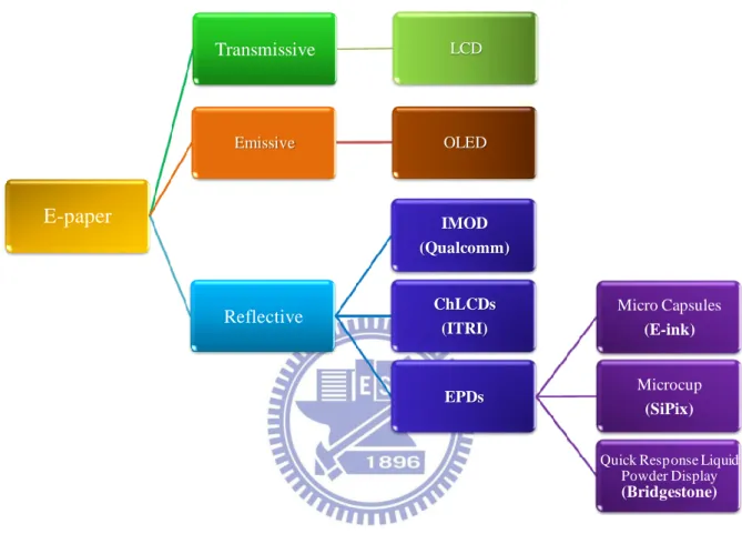
1.1 Classification of E-papers
E-papers can be classified into three major types, the transmissive, emissive and reflective types as shown in Fig. 1-2.
Fig. 1-2 E-paper classification.
The transimissive and emissive types function as liquid crystal displays (LCDs) or organic light emitting diodes (OLEDs) having 256 gray levels, high contrast ratio and fast response time which make them possible to play videos as shown in Table 1-1. However, LCDs have narrower viewing angle, higher power consumption, lower stress endurance and less flexible compare to the reflective types. The OLEDs, on the other hand, have better viewing angle, lower power consumption, higher stress endurance and flexibility but the power consumption are still higher than the reflective types. Moreover, the transmissive and emissive types are less comfortable for human-eye perception in long term utilization and under sun light.
E-paper Reflective EPDs Micro Capsules (E-ink) Microcup (SiPix)
Quick Response Liquid Powder Display (Bridgestone) ChLCDs (ITRI) IMOD (Qualcomm) Transmissive LCD Emissive OLED
3
By contrast, the paper-like property of reflective types makes them better choices for human-eye perception. The reflective types include electrophoretic displays (EPDs), cholesteric liquid crystal displays (ChLCDs) and interferometric modulator displays (IMODs). IMODs are less flexible while the others have better endurance and flexibility. Most important of all, the bistability characteristic enables image to be retained after removing off the applied electric power which highly decreases the power consumption. As a result, for eye-friendly and power saving points of view, the reflective types have become the mainstream in the market of E-papers.
Table 1-1 Classification of transmissive, emissive and reflective types EPDs [1].
For the market potential of flexible displays, the EPDs and ChLCDs of the reflective types are more suitable. They both have wide viewing angle, good flexibility, endurance and power saving ability. The major difference between EPDs and ChLCDs is the materials being driven, which are charged particles and the cholesteric liquid crystal, respectively.
The cholesteric liquid crystal has bistability in both planar and focal conic states as shown in Fig. 1-3. Specific wavelengths of light are reflected in the planar texture to reveal
Types Transmissive Emissive Reflective
Classification LCD OLED IMOD ChLCDs
EPDs Microcapsule QRLPD Microcup Reflectivity ~30% 25~30% 35~40% ~30% 25~30% Viewing angle 120~140° 170~180° ~160° ~160° ~180° ~180° ~180° Transition time (ms) 40 0.01 1 20 300~500 0.2 300~500 Driving voltage 5~30V 2~10V <5V ~80V ±15V ~70V ±15V
Driving type AM/PM AM/PM AM AM/PM AM/PM PM AM/PM
Color realization Filter Filter MEMS Solvent Filter Filter Solvent
Gray level number 256 256 254 64 16 16 16
Contrast ratio 200~400:1 200~300:1 ~9:1 > 10:1 10:1 10:1 10:1 Video ◎ ◎ ◎ ◎ X X X Power saving X △ ◎ ◎ ◎ ◎ ◎ Flexibility △ ◎ △ ◎ ◎ ◎ ◎ Endurance X ◎ △ ◎ ◎ ◎ ◎ Large-size △ △ △ ◎ △ △ △ Manufacture cost ◎ △ △ ◎ △ △ ◎
Company Fuji Xerox
Fujitsu
Mitsubishi Kodak Philips
Qualcom
4
the bright state, while lights transmitted and scattered in the focal conic texture and reveals dark state. The ChLCDs are manufactured by roll-to-roll process which lowers the cost, and are colorized by mono-layer of RGB cholesteric liquid crystal filled or inject-printed into the cell which is color filter free. Moreover, the mono-layer makes the displays more flexible and endurable of stress and easier for alignment. Although the response time of ChLCDs is 1/10 of EPDs, the higher operating voltage remains an issue.
Fig. 1-3 Three states of cholesteric liquid crystal display [2].
There are mainly three types of EPDs, the microcapsules, microcups and the quick response liquid powder display (QRLPD). Of all types of EPDs, the QRLPD have the same high operating voltage issue like the ChLCDs, while the microcapsule and the microcups have lower operating voltages but lower response time. Among all types of EPDs, the microcup EPD has its advantages of low manufacturing cost using roll to roll process [3][4] and high color saturation realized by color solvent instead of color filters.
1.2 Prior Arts of Electrophoretic Displays (EPDs)
The EPDs share similar advantages such as not suffer from serious light reflection under sun light and has wide viewing angle, low power consumption, flexibility, and applicable onto virtually any surface, including glasses, plastics, fabrics and, even papers. Still, there are some
5
differences among them which are listed below.
1.2.1 Microcapsule EPD
The microcapsule EPD also called electronic ink is made up of millions of micro-meter capsules. Each microcapsule contains positively charged white particles and negatively charged black particles suspended in a transparent fluid as shown in Fig. 1-4. When applying an electric field, corresponding particles move to the opposite charged electrodes and top of the microcapsules are visible to the user. This makes the surface appear white or black. However, it has some shortcomings as low response time and high manufacturing costs.
Fig. 1-4 A Microcapsule EPD structure[5].
1.2.2 Quick Response Liquid Powder Display (QRLPD)
A QRLPD contains negatively charged white particles and positively charged black particles suspended in the air as shown in Fig. 1-5. When applying an electric field, corresponding particles move to the opposite charged electrodes and the user can see gray levels according to mixture of two colored particles.
Moreover, the response time is faster than average LCDs. However, because of the high operation voltage, it can only be implemented on passive matrix driving displays. Besides, it has color realization and high manufacturing cost issues.
6
Fig. 1-5 A QRLPD structure [6].
1.2.3 Microcup EPD
The Microcup EPD is made up of matrix of cups typically 150μm in width. The whole display has strong strengthens because of the microcup structure which is more applicable in flexible displays and fits into roll to roll manufacture. It can be made square or hexagon as shown in Fig. 1-6.
Fig. 1-6 A Microcup EPD structure [7].
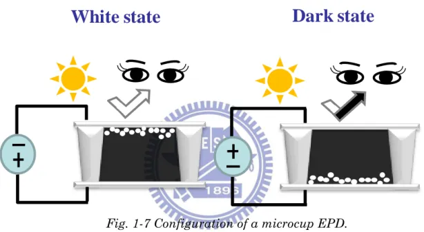
The optical contrast of a microcup EPD is varied by manipulating the position of electrically-charged particles (white) inside the fluid (black) [8] as shown in Fig. 1-7. When the white positively charged TiO2 particles are driven to the upper electrode, the
7
observer sees white state. When particles are driven to the bottom electrode, the light is scattered and absorbed by the black fluid so the observer sees dark state.
Although the transition time of a microcup EPD is not fast enough compared to the QRLPD, the microcup EPD has lower manufacturing cost due to roll-to-roll process and color can be realized by color solvent instead of inefficient color filters, which increases the overall whiteness. Therefore, the microcup EPD was chosen to be our research objective.
Fig. 1-7 Configuration of a microcup EPD.
1.3 Motivation and Objectives
Research has been done from the aspect of optical response only to simulate particle motion in EPDs. M. A. Hopper and V. Novotny in 1979 treated the optical off-response of an EPD using a model employing transport of charged particles [9]. However, little is known about the motion of various charge species inside the EPDs. Therefore, to understand the contribution of different charge species and their motion of voltage dependence, both current and optical responses were taken into account in this thesis. Some experiments were designed to test and verify the hypothesis. Furthermore, fundamental characteristics of microcup EPDs will be discussed, including the charging and driving mechanisms, the contributors involved
8
when driving and without driving and some criteria that influence the performance. As noted that the transition time for the EPDs is not fast enough so the methods are proposed and verified to reduce the transition time and shortened driving waveforms are designed based on the physical mechanisms.
1.4 Thesis Organization
The thesis is organized as follows: the fundamental properties, the charge and bistability mechanisms of a microcup EPD are introduced in Chapter 2. Besides, the instruments used in the experiment are described in Chapter 3. The proposed model and experimental results are discussed in Chapter 4. Finally, conclusion, minor issues and the future work are presented in Chapter 5.
9
Chapter 2
Mechanisms
This chapter introduces the charge and bistability mechanisms, including how TiO2
become positively charged, the charge species who contribute to the current in the micro-cups and how they stabilize in the suspension. Then is the understanding of some primary colloid science, such as the double layer and the zeta potential that associated with the bistability. Some notable optical characteristics like wake-up time (WUT) and paging time will also be elaborated. In the end, the criteria of EPD performances will be introduced
2.1 Mechanism of Charged Particles
The charged particles are prepared with the TiO2 pigments mixing with the surfactants in
the non-polar solvent. Pigments become positively charged after chemically adsorption of surfactant molecules [10]. Upon applying an external field, the surfactant molecules dissociate into a pair of oppositely charged species as shown in Fig. 2-1 (a) [11][12]. T. Bert and H. De Smet in 2005 described how the charged species can be stabilized in the non-polar solvent is the formation of micelles, as shown in Fig. 2-1 (b) [13]. Also, part of the charged species would interact with pigments to make them charged (Fig. 2-1(c)). The charged shells help to avoid the flocculation between particles, which thus increases the dispersion stability [14]. While applying an external field, both charged particles and dissociated ions would contribute to the current in the EPD device, which will be thoroughly discussed in 0.
10
(a) (b)
(c)
Fig. 2-1 Formation of (a) surfactant dissociation (b) micelle, and (c) particle configuration inside the microcup EPD [15][16].
2.2 The bistability Mechanism
There are two main reasons why we choose EPDs instead of LCDs as E-books. One is that EPDs have no viewing angle and glare issues as LCDs does, which provide more comfortable visual experience. More importantly, EPDs have bistability characteristic, i.e. the image can be retained without supplying a power voltage and makes E-books more eco-friendly. The factors explaining how particles be stabilized in the solvents will be discussed thoroughly in the following sections.
2.2.1 Colloid Behavior
The particles inside the microcup EPD are also called colloids which are suspended in solvents. Without applying voltages, charged particles tend to repel each other, while the uncharged particles are free to collide and aggregate. To obtain stable colloid suspensions, there are some options to modulate such as:
i. Viscosity
In some cases, an in-between condition of weak aggregation causes viscosity to be a function of shear rate. For example, stirring produce enough shear to reduce the viscosity and promote blending such as paints.
+
+_
Surfactant dissociation
micelle
particle
11
ii. Surface forces
The surface forces at the interface of particles and solvents should be considered both electrostatic repulsion forces and Van der Waals attraction forces. Colloids with opposite charges tend to agglomerate and form an interconnected matrix. On the other hand, the same charged colloids are likely to repel each other and remain discrete or dispersed in the suspension if the charge is high enough.
Particle charges can be controlled by modifying the pH of solvent or changing the ionic species in solution. More directly, to use surface active agents, such as surfactants, who adsorb to the surface of the colloid and change its characteristics as mentioned in 2.1.
2.2.2 The Electric Double Layer and Zeta Potential
In the colloidal field, the electric double layer is often used to visualize neighboring ionic environment of a charged particle and to explain how repulsive forces occur. Corresponding to Fig. 2-2, the negatively charged TiO2 colloid first attracts a high
concentration of adjacent positive ions in solution. This high density layer of positive ions is known as the Stern layer.
Additional positive ions are continuously attracted by the negative colloid outside the Stern layer but with lower concentration because of the repulsion force from same positive charges in the Stern layer. The dynamic equilibrium results in the formation of a loosely associated layer, which is named as the diffuse layer. It is made of free ions which move in the fluid under the influence of electric attraction and thermal motion rather than being firmly anchored.
Unlike the Stern layer consisting of only positive ions, the diffuse layer contains both positive and negative ions with different trends. While the positive ion concentration gradually decreases with increasing distance from TiO2 surface, the
12
negative ion concentration gradually increases as the repulsive forces from the TiO2 are
electrically screened by the positive ions.
Fig. 2-2 Scheme of the ion distribution around the charged particle. The gray circle is the charge density around TiO2, the darker the denser.
The Stern layer and the diffuse layer are referring to as the double layer. The double layer is formed to neutralize the charged colloid, which in turn causes an electro-kinetic potential between the surface of the colloid and any point in the suspension. The voltage difference is on the order of millivolts. The particles mobility is related to the dielectric constant and the viscosity of the suspension and to the electrical potential at the boundary between the moving particle and the liquid as shown in Eq.2-1. The boundary is often called slipping plane. The electrical potential at this junction is called zeta potential.
13 r 0 e (2-1) whereris the dielectric constant of the dispersion medium, ε0 is the
permittivity of free space (C² N−1 m−2), η is dynamic viscosity of the dispersion medium (Pa s), and ζ is zeta potential (i.e., the electric potential of the slipping plane in the double layer).
The Debye length, usually denoted with symbol κ−1, is the distance between the slipping plane and the particle surface, which is proportional to the square root of temperature and reciprocally proportional to the square root of the ion concentration as shown in Eq. 2-2. I T r 0 1 (2-2)
Where T is the temperature, I is the ion concentration, i.e., the concentration of ions in the dispersion medium.
The thickness of Debye length decreases with increasing ion concentration in the dispersion medium. When zeta potential is low, attraction exceeds repulsion and the dispersion will break and flocculate. So, colloids with high zeta potential are electrically stabilized while colloids with low zeta potentials tend to coagulate or flocculate. The net interaction curve is shown in Fig. 2-3.
14
Fig. 2-3 The net interaction curve of attractive and repulsive forces around the colloid [16].
2.2.3 Amplitude of Multiple Forces
The bistability characteristics come from the balance of multiple forces. Take the microcup EPD for example, the order of each force and their causes are listed in Fig. 2-4. When electric field is applied, the order of Coulomb force is at least three times of the other forces so that the applied field dominates particle motion. When removing the applied voltage, the dominator comes to the inverse induced internal field whose magnitude is decided by the pulse width and magnitude of the applied voltage. The strength of the inverse induced internal field decreases with increasing time so the other forces come into play and affect long term bistability. The Van der Waals force is an attractive force between particles while the electrostatic force acts as the repulsive force. These two forces are dynamically equilibrium. Similarly, the buoyancy, gravity and the viscosity come to dynamically equilibrium as buoyancy and gravity struggle with each other and the viscosity retards particle from motion. The Brownian motion is determined
15
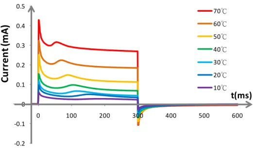
by the temperature at all time. When temperature is high, particles are more unstable and tend to move, i.e. poor bistability, but faster transition time and higher current as shown in Fig. 2-5. Relatively, when temperature is low, particles are less influenced by Brownian motion and are more stable, which brings about smaller current under the same applied pulse voltage. More detail about current contributors can be found in 0.
Fig. 2-4 Force category inside a microcup EPD [18][19].
Bistability
Coulomb 10-10 Van der Waals 10-13 Electrostatic 10-13 Gravity 10-15 Buoyancy 10-15 Viscosity 10-15 Brownian motion _temperature16
Fig. 2-5 Current response at different temperatures (the same pulse width of an applied voltage in 300ms of 15V).
2.3 Optical Characteristics
2.3.1 Wake-up time (WUT)
When applying a pulse voltage, the optical response of an EPD does not respond immediately. Instead, there is duration from the start of the applied voltage to the rise or fall of optical response. This threshold-like behavior is called the wake-up time (WUT) as shown in Fig. 2-6. This duration is interpreted as the time required for different lightness being perceived.
The wake-up time varies by different circumstances, such as temperature in Fig. 2-5. Further discussion can be found in Chapter 4
-0.2 -0.1 0 0.1 0.2 0.3 0.4 0.5 -100 0 100 200 300 400 500 600 70℃ 60℃ 50℃ 40℃ 30℃ 20℃ 10℃
C
u
rr
e
n
t (
m
A
)
t(ms)17
Fig. 2-6 Wake up time [20].
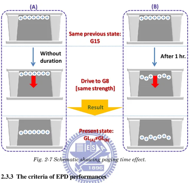
2.3.2 The paging time
The paging time refers to the duration between previous image and present image. The paging time will affect gray level accuracy when the image stability is not good, for instance, easy to aggregate or hard to be dispersed in the solvent which result in faster degradation of lightness. For a poor bistability film, Fig. 2-7 shows the driving with and without a paging time of 1-hr duration from white state to middle gray level. Fig. 2-7 (A) is direct drive from previous white state to middle gray level; Fig. 2-7 (B) is white state waiting for an hour and then driven with the same strength. The result shows that different duration leads to different end positions. Thus, the paging time should be taken into consideration for achieving gray level accuracy. Moreover, the paging time is related to the current and wake-up time, which will be discussed in Chapter 4.
18
Fig. 2-7 Schematic showing paging time effect.
2.3.3 The criteria of EPD performances
Besides usual judging standards such as brightness and contrast ratio, there are three major criteria that relate to the EPD performances including:
i. Transition time
The time required for particles to transit from one electrode to another. The usual transition time for a Microcup EPD is about 300ms which is almost 10 times of the LCD response time and is the reason why a normal EPD incapable of playing videos.
ii. Bistability
The time that image can sustain in the same grey level without applying voltage as shown in Fig. 2-8. For a display with good bistability, the image can sustain in the same grey level without applying voltage for a long time. However, for a display with
After 1 hr.
Present state:
GL
(A)≠GL
(B)Drive to G8
[same strength]
Without
duration
(A)
(B)
Same previous state:
G15
19
poor bistability, the lightness will degrade easily after removal of voltage. For a poor bistability film, the paging time as mentioned in section 2.3.2 will affect the grey level accuracy enormously. Usually, the bistability is decided by the material science such as the surfactants or the type and concentration of the suspensions.
Fig. 2-8 Lightness degradation because of poor bistability.
Fig. 2-9 Lightness deviation through time for different waveforms.
However, the driving waveform also plays an important role in the bistability characteristics. For example, the lightness degradation by different waveforms, a 10s pulse and a symmetric waveform, is shown in Fig. 2-9. In this experiment, we see how waveforms can influence the image bistability. The 10s pulse suffers from poor
duration
0 5 10 15 20 25 30 35 0 100 200 300 400 500 600∆L*
symmetric WF 10s DCt(s)
ΔL*
20
bistability because of excess ions would affect the Debye length, as mentioned in section 2.2.2, which then affect the bistability.
iii. Grey level accuracy
Grey level inaccuracy has two main factors as shown in Fig. 2-10. One is because of poor bistability that results in the lightness deviation from different paging time as mentioned in 2.3.2. To solve this issue, enhancing the bistability is the best way. Second is the image history effect which results in the ghost image as shown in Fig. 2-11. The ghost image is generated from the influence of previous states. The ghost image is often solved by inserting the shaking waveforms before the driving waveform to erase the history as shown in Fig. 2-12. First, to active the particles from image sticking issue, i.e., charged particles stick to the boundaries of the cells, or to erase the influences from previous states, a shaking waveform is applied. Second, in order to have a uniform start condition, a reset pulse is applied to push all the particles to one boundary. Finally, the driving waveform is applied after further shaking waveform.
Fig. 2-10 Classification of Grey level accuracy factors.
GL
accuracy
Paging
time
Lightness
deviation
Image
history
Ghost
image
21
Fig. 2-11 Ghost image.
Fig. 2-12 The shaking waveform used to solve the ghost image issue.
2.4 Summary
To get the best performances as mentioned in the last section, most companies tune their waveform only by observing the optical responses which can only distinguish the macroscopic variation of lightness, that is, incapable of knowing the physical mechanisms inside the cell. On the other hand, the current response can help to understand the motion of charged species which is the major factor that dominates the criteria of EPD performances. Therefore, to understand the physical mechanism inside the micro-cup, both optical and current responses were synchronized. Furthermore, the experimental setup and instruments are discussed in the next chapter..
V
t
22
Chapter 3
Instruments
The study mainly focuses on the analysis in both current and optical responses. To get all these responses, some instruments are needed, such as the photo-diode, which was used for quantize optical response; the current meter, used for measuring current response; the driving box, used for applying electric signals to the micro-cup film, and etc. In this chapter, the experimental setup and instruments used in this study are illustrated.
3.1 Experimental Setup and Instruments
3.1.1 Experimental Setup
Both current and optical responses are considered to analyze the physical mechanism in this thesis. The experimental setup is shown in Fig. 3-1. A 632.8 nm wavelength He-Ne LASER was used as the light source. Different waveforms were supplied by a driving box. When the microcup film received the signals from the driving box, different gray levels were shown. Then the lambertian reflected light was captured by the photo-diode to quantify gray levels. In the meanwhile, current response was captured by current meter.
23
Fig. 3-1 Experimental setup for measuring current and optical responses.
3.1.2 Driving box
Different waveforms were written into the driving box before applying signals to the microcup film. The driving box as shown in Fig. 3-2 was provided by SiPix. Waveforms were written into the driving box by using MPLAB ICD 3 as shown in Fig. 3-3. The written signals should include both voltages of top and bottom electrodes. Usually, signals are written in “H” and “L”. “H” refers to high and represents +30 volt in our experiment. “L” refers to low and represents 0 volt. If the top electrode is “H” and bottom electrode is “L”, then the positively charged particles move towards the bottom electrode so the film appears black. If the top electrode is “L” and the bottom electrode is “H” then the film appears white. If the top and bottom are both “H”, “H” or “L”, ”L” then it means “do nothing”, i.e. particles will not move.
Photo-diode:
He-Ne LASER
Lambertian reflectance
Current meter:
Recording with time
Optical Response Current Response
Driving Box:
Apply Waveforms
24
Fig. 3-2 The picture of the driving box.
25
3.1.3 Photo-diode
The collimated light source in Fig. 3-4 is a He-Ne laser with model number of LGK 7672 manufactured by ONSET electro-optics Co., output 5mW. Therefore, the light intensity of the laser light source is capable of being detected by the photo-diode after passing through some distances. To obtain reliable experimental data, the laser intensity is calibrated and shown in Fig. 3-5.The laser takes about 25 minutes to a steady intensity state for an experimental measurement.
The photo-diode is manufactured by THORLABS Inc. with model number of PDA100A. It is an amplified, switchable-gain, silicon detector designed for detection of light signals over 350~1100 nm wavelength range, which is sufficient enough in our experiment. The active area of the photo-diode is 9.8mm in diameter which is suitable for detecting lambertian reflectance from the film. The photo-diode is used to quantify gray levels of a microcup EPD film. It transforms light signals to electric signals by photoelectric effect. The optical response is the Lambertian reflectance of the film with an unit of mV. Because it is a relative value, it is shifted for chart convenience afterwards.
Fig. 3-4 The setup for optical response measurement.
Photo-diode
He-Ne LASER
Microcup EPD film
Lambertian
reflectance
26
Fig. 3-5 Calibration of the He-Ne LASER.
3.1.4 Current meter_ Keithley
The model 6485 picoammeter is manufactured by Keithley Instruments, Inc. as shown in Fig. 3-6. The current magnitude in our experiment is about 0.01mA to 0.01nA and is below 50Hz. The acquisition range is from 20fA to 20mA, and the sampling rate is up to 1000 Hz, which provides sufficient accuracy in our measurement.
The Keithley needs aided software, the ExceLINX, to operate. The sampling rate, measurement range, etc. can be tuned in ExceLINX. Instant measured current data is recorded by connecting film and the current meter in series.
Fig. 3-6 The picture of Keithley current meter. 310 315 320 325 330 335 340 345 0 5 10 15 20 25 30 35 t(min.)
O
p
ti
c
a
l
re
s
p
o
n
s
e
(m
V)
http://www.testequipmentconnection.com/images/products/KEITHLEY_6485.JPG27
3.1.5 Colorimeter_i1
The illumination of i1is a bulb with the spot size 3.5mm and the scan rate is 200Hz. It is capable of measuring color coordinates and also the spectrum. Because the optical response can only shows the relative value of lightness, the i1 colorimeter purchased from HomDa Automation Co., Ltd. shown in Fig. 3-7 is used to acquire the absolute brightness of the film in our experiments. Before measuring the lightness of the micro-cup film, calibration was done in advance by the attached standard white. The average lightness of a microcup EPD is 68watt/cm^2 at white state and is 24 watt/cm^2 at dark state.
Fig. 3-7 The photo of i1.
28
Chapter 4
Experimental results and Application
The micro-cup films were sensitive to temperature and humidity so all experiments were conducted at constant temperature and humidity (20℃ and 55%). First, a model for motion of internal charged species was proposed based on the observation of both optical and current responses. Furthermore, different waveforms including pulse and symmetric waveforms were tested to verify the model and to understand the physical mechanisms inside the microcup EPDs. Correlation between emergence of current bump and wake up time were also testified. Finally, the application under the basis of observed physical mechanisms for designing shorter driving waveform was proposed in this chapter.
4.1 Three current states
To understand the physical mechanism inside the microcup EPD, both current and optical responses are taken into consideration in the experiments. Based on the hypothesized dominant contributors from particles or dissociated ions as mentioned in 2.1, the current response is divided into three parts, including transient current (stage I), intermediate-state current (stage II), and the discharge current (stage III) as shown in Fig. 4-1.
Upon applying an external field of a 300ms, 30V pulse voltage, the transient current (stage I) responded instantly, whereas the optical response remained almost unchanged. This indicates that the transient current peak is dominated by the dissociation of surfactants instead of the dispersed particles corresponding to Fig. 4-2(b). With continuous application of the external field, the ions and other charged species accumulated at the electrode, so a space charge region is formed, corresponding to Fig. 4-2(c). This region does not contribute to the current; also, it screens out the applied voltage which results in the decrease of transient current [21][22].
29
In the stage II, a bump appears after the wake-up time in the intermediate-state current with the steepest optical response. This indicates that dispersed particles have accumulated enough energy to move to the opposite electrode, corresponding to Fig. 4-2(d). Consequently, the dominant contributor of the current bump in the intermediate-state is the particles.
After releasing the applied voltage, the optical response does not drop, but a reverse current peak appears at the stage III. This implies that the induced internal electric field inside the microcup pushes the lighter dissociated ions away from the electrodes, whereas the heavier charged particles remained the same position with this induced electric field, corresponding to Fig. 4-2(e).
In the following chapter, these assumptions will be tested and verified from both optical and current responses for different waveforms with same current trends.
Fig. 4-1 Current and optical responses of a 30V, 300ms pulse voltage applied. The green line is the applied voltage (V); the blue dash line and red line are the current and optical response (OR), respectively. The unit of optical response is measured by photo-diode with the unit of mV.
-0.14 -0.10 -0.06 -0.02 0.02 0.06 0.10 0.14 -60 -40 -20 0 20 40 60 -100 0 100 200 300 400 500 600 OR V current
t(ms)
Current (mA)
Applied voltage (V)
Optical response (mV)
Wake Up Time (WUT)
I
II
III
bump
L*=24
30
Fig. 4-2 Flow chart of charges inside the microcup EPD. The red signs are the applied voltages. The big white and the tiny black circles are particles and ions, respectively.
4.2 Current Bump with Various Pulse Widths
Four different pulse widths including 100ms, 150ms, 200ms, and 300ms of a 30V applied voltage were designed to observe the relationship between current bump and pulse widths as shown in Fig. 4-3(a).
The experimental result shows that:
I. Different pulse widths with same wake-up time (about 90ms). This reveals that the wake-up time is dominated by initial applied voltages; that is, the charges feel the identical strength during the preceding 100ms of all four applied widths.
II. Current bumps in different pulse widths were fixed at the same position (approximately 180 ms). Moreover, the current bump always occurs after the wake-up time with the dramatically rising of optical response. That was, the current bump came from the movement of dispersed particles as assumed in the previous section. Therefore, the optical response curves with 100 ms (blue curve) and 150 ms (green curve) pulse widths did not reach an extreme white state because the pulse widths were not long enough to drive particles completely, so that the bump did not happen in time.
Initial: K Final: W Screening field (a) (b) (c) (d) (e) (f)
E
internal31
From the current point of view, the overlapping of these four current curves further showed the sum of generated currents, i.e. from particle motion and dissociation of surfactants, was similar under the same voltage amplitude and period of different pulse width voltage modulations.
III. When a pulse width was longer, surfactant dissociation rose accordingly and resulted in a higher discharge peak current, as shown in stage III. The experimental results concluded that the transient currents (stage I) and discharge current peaks (stage III) were both generated by micelles or ions because of the retained optical response. The longer the pulse width, the larger amount of surfactant molecules dissociated and larger internal electric field induced. Therefore, discharge current peak at 300ms pulse width was larger than the peaks at 200ms, 150ms, and 100ms. Furthermore, the amplitude of discharge-current peak was less than half of the transient-current peak, which indicated that most of the ions and micelles remained near the electrode, while part of them being pushed away by the internal induced electric field and recombined together [23].
The reverse voltage experiment also revealed similar experimental results as shown in Fig. 4-3(b). The major difference in the opposite magnitude experiments was that the wake-up times of white to dark state were about 60ms, which was 30ms shorter than that of dark to white state (Fig. 4-3(a)). There were three possible reasons: First, different materials at top and bottom surfaces of a microcup, which bring about different strength of particle-surface interaction. So the wake-up times would be different. Second, because the geometrical shape of the microcup is asymmetric as shown in Fig. 1-7, which leads to different particle distribution, and with more particles closer to the boundary and affected by particle-surface interaction, wake-up time would be longer. Third, gravity acted as different factors on the top and bottom of a microcup. When particles are on the top of the microcup, i.e. at initial white state, both the applied electric field and gravity contribute to the forces that push charges away from the top electrode.
32
Therefore, white to dark state required less time to respond to the applied voltage, in other words, shorter wake-up time was needed. Even so, the largest change of optical response was still at the bump position. This strong correlation is the most interesting finding in this experiment.
(a)
(b)
Fig. 4-3 Current and optical responses of a microcup EPD modulated by four different pulse widths of 100ms, 150ms, 200ms, and 300ms durations with voltages
-0.12 -0.08 -0.04 0.00 0.04 0.08 0.12 0.16 0.20 -60 -40 -20 0 20 40 60 -100 0 100 200 300 400 500 600 t(ms) C u rr e n t (m A ) O p ti c a l re s p o n s e (m V) OR current
K(initial state) → W(final state)
-0.20 -0.16 -0.12 -0.08 -0.04 0.00 0.04 0.08 0.12 -60 -40 -20 0 20 40 60 -100 0 100 200 300 400 500 600 t(ms) C u rr e n t (m A ) O p ti c a l re s p o n s e (m V)
33
(a) 30V (initial in the dark state) and (b) -30V (initial in the white state). The solid line represents the optical response and the dash line is the current.
Single pulse experiment is fundamental for realizing the motion of charge materials inside a microcup. However, the driving waveforms are generally combined by series of pulses. Following, the optical and current responses using various driving waveforms are further studied.
4.3 Current Bump with Symmetric Waveforms
To further figure out the correlation between a bump position and optical response, a series of symmetric voltage waveforms were designed. Because the bump appears at the dramatically rise/fall of optical response, one may expect to see it appears near 180ms in the second phase of a symmetric waveform as it did in the single phase in Fig. 4-3
An interesting finding in this experiment, there was no current bump at the second pulse, i.e. position of plus/minus voltage transition as shown in both Fig. 4-4 (a) and (b). The current response results were compared with a single pulse voltage applied on an EPD as shown in Fig. 4-1. The transient peak current (peak A) at the first pulse and the discharge peak current (peak C) at the second phase of a symmetric waveform have almost the same current magnitude as that of applying a single pulse voltage (0.14 mA and 0.04 mA, respectively) in Fig. 4-1. The results further verified the transient and discharge currents were mostly contributed from surfactant disassociation. The current magnitude would be the same with the amount of applied voltages as discussed in the part ii of section C. However, a current (0.18 mA) of the peak B was 28% larger than the first transient current of peak A (0.14 mA). The peak B was almost the addition of transient peak A and the bump in magnitude. Consequently, we speculated that the peak B is the superposition of currents contributed from both dispersed particles and ions.
34
(a)
(b)
Fig. 4-4 Symmetric waveforms for (a) 300ms, 30V plus 300ms, -30V. (b) 300ms, -30V plus 300ms, 30V. Red solid curve is the optical response (OR), green solid square is the applied voltage (V), and the blue dashed curve is the current response.
For a single pulse as mentioned in 4.1, the dispersed particles and ions moved to the collecting electrode when a voltage was applied. After releasing the voltage, ions were pushed away from the electrode because of a repulsive force by an induced internal electric field. After the relaxation time, as more ions left the electrode, spaces around the particles were spared, i.e., particles felt less repulsive force from the neighboring charges when removing the applied voltage as shown in Fig. 4-5.
-0.20 -0.16 -0.12 -0.08 -0.04 0.00 0.04 0.08 0.12 0.16 0.20 -60 -40 -20 0 20 40 60 -200 0 200 400 600 800 1000 OR V current t(ms) C u rr e n t (m A ) A p p li e d v o lta g e (V ) O p ti c a l r e s p o n s e (m V) A B C -0.20 -0.15 -0.10 -0.05 0.00 0.05 0.10 0.15 0.20 -60 -40 -20 0 20 40 60 -200 0 200 400 600 800 1000 t(ms) C u rr e n t (m A ) A p p li e d v o lta g e (V ) O p ti c a l r e s p o n s e (m V) A B C
35
Fig. 4-5 Flow chart of charged-specie motion when removing electric field. In the symmetric waveform, however, there was no removal voltage in the second phase but giving a reverse voltage instead. At this moment, the electric force fr om the induced internal and the applied external electric fields were in the same direction as shown in Fig. 4-6, which accelerated the charged materials, just like some active and hurried people push each other while leaving a musical concert. Therefore, the positive charges felt an instant stronger repulsive force while the voltage was reversed. This explained the higher current amplitude of peak B compared to that of peak A and implied that a bump may thus hide inside the peak B as we speculated in the last paragraph.
Fig. 4-6 Flow chart of charged-specie motion at B in Fig. 4-4 (b)
If the speculation is true, the current bump will emerge again once there is enough time for ion relaxation. A new waveform is design to be beneficial for ion relaxation in the next chapter
4.4 Symmetric Waveforms with an In-between Inserted duration
To verify that a bump is buried in peak B and a higher peak B current amplitude comes from the sum of a discharge current of the first phase (lack of relaxation time) and a transient current of the second phase, symmetric waveforms separated by various durations were
E
internalE
internalE
36
designed as shown in Fig. 4-7. If a duration provides charges with enough relaxation time, the bump in the second phase is expected to appear again.
Fig. 4-7 A symmetric waveform with sequential pulses of 300ms/30V, a duration t/0V, and 300ms/-30V.
Four durations were tested, including t = 40 ms, 300 ms, 500 ms, and 1000 ms. Fig. 4-8(a) shows that the current bump emerges after 500 ms. Furthermore, the wake-up time shows the same trend in Table 4-1. Below 500ms, a wake-up time increased with an increasing duration, and came to a stable value after the duration of 500 ms. The result implied that the shorter duration, the shorter transition time but less ion relaxation. The reverse voltage experiment presented the same result as shown in Fig. 4-8(b). This result indicated that the bump’s emersion not only related to the degree of ion relaxation, but also correlated with the length of wake-up time and transition time. Moreover, the wake-up time is almost zero without a duration (symmetric waveform as Fig. 4-4), this may be served as a method for shortening the driving time afterwards.
-40 -30 -20 -10 0 10 20 30 40 -0.3 0 0.3 0.6 0.9 1.2 1.5 V t(s) A pp lie d vo lt age (V )
duration
37
Fig. 4-8 Durations at 40ms, 300ms, 500ms and 1000ms from top to bottom. A symmetric waveform with sequential pulses of (a) 300ms/30V, a duration t/0V, and 300ms/-30V. (b) 300ms/-30V, a duration t/0V and then 300ms/30V.
-0.20 -0.15 -0.10 -0.05 0.00 0.05 0.10 0.15 0.20 -60 -40 -20 0 20 40 60 -500 0 500 1000 1500 2000 -0.20 -0.15 -0.10 -0.05 0.00 0.05 0.10 0.15 0.20 -60 -40 -20 0 20 40 60 -500 0 500 1000 1500 2000 -0.20 -0.15 -0.10 -0.05 0.00 0.05 0.10 0.15 0.20 -60 -40 -20 0 20 40 60 -500 0 500 1000 1500 2000 -0.20 -0.15 -0.10 -0.05 0.00 0.05 0.10 0.15 0.20 -60 -40 -20 0 20 40 60 -500 0 500 1000 1500 2000 -0.20 -0.15 -0.10 -0.05 0.00 0.05 0.10 0.15 0.20 -60 -40 -20 0 20 40 60 -500 0 500 1000 1500 2000 -0.20 -0.15 -0.10 -0.05 0.00 0.05 0.10 0.15 0.20 -60 -40 -20 0 20 40 60 -500 0 500 1000 1500 2000 -0.20 -0.15 -0.10 -0.05 0.00 0.05 0.10 0.15 0.20 -60 -40 -20 0 20 40 60 -500 0 500 1000 1500 2000 -0.20 -0.15 -0.10 -0.05 0.00 0.05 0.10 0.15 0.20 -60 -40 -20 0 20 40 60 -500 0 500 1000 1500 2000 t(ms) Optical response (mV) 40ms 40ms 300ms 300ms 500ms 500ms 1000ms 1000ms
OR
current
(a)
(b)
38
Table 4-1 Wake-up time (WUT) for symmetric waveform with duration t inserted between two phases
Four pulses of the second phase in Fig. 4-8(a) are shifted and piled up together as shown in Fig. 4-9. The current bump gradually appeared with an increasing duration time. The experimental result indicated the bump is buried in the second pulse. Additionally, when the duration is long enough (500 ms at this experiment) for the ion relaxation, current bump emerges.This result also indicated if the bump position appeared earlier by different voltage waveforms, then the optical response time can be shortened.
Fig. 4-9 Overlap three inverse pulses in Fig. 4-8(a) (Four experimental time axes are shifted for comparison convenience).
4.5 Application
The current bump represents the moment of complete transition to the extreme state as
Duration t(ms)
0
40
300
500
1000
WUT
(ms)
W→K
4
4
44
64
64
K→W
4
8
68
90
90
-0.18 -0.14 -0.1 -0.06 -0.02 0.02 0.06 -100 0 100 200 300 400 500 600 700 800 1000ms 500ms 300ms 40ms-0.02
C
u
rr
e
n
t (
mA
)
t(ms)
600Bump shift
39
mentioned in 4.2, the symmetric waveform can reduce the transition time in 4.3, and the optical response time can be reduced if the bump position appears earlier by different voltage waveforms in 4.4. Combining these three experimental results, a waveform for shortening driving time was designed as shown at the right-hand side in Fig. 4-10. A short reverse pulse was inserted before the original one, and the original phase was reduced to the timing that optical response came to the extreme state.
The designed waveform meant to reduce the effect of wake-up time, thus shortened the transition time. Besides, the reverse pulse should not change the original optical state, i.e., the optical response remained the same amplitude, so that the waveform can be shortened without a luminance changed.
Fig. 4-10 Schematic showing for reducing transition time.
Comparison between a 300 ms pulse and the proposed waveform (a 20 ms negative pulse width inserted before the 300 ms positive pulse width) is shown in Fig. 4-11(a). The experimental results showed the designed waveform reduced 50 ms of both the wake-up time and the transition time. Besides, the total driving time is reduced from 250 ms to 200 ms (20% improved). The inverse experiment also showed the similar result as shown in Fig. 4-11(b). However, the wake-up time did not change obviously. The reason may be the difficulty of measuring lightness change in the dark state. The dark fluid in a microcup adsorbed scattered light which may be one of the reasons why observing the lightness change from the white state

![Table 1-1 Classification of transmissive, emissive and reflective types EPDs [1].](https://thumb-ap.123doks.com/thumbv2/9libinfo/8448237.182325/15.892.142.801.476.889/table-classification-transmissive-emissive-reflective-types-epds.webp)
![Fig. 1-6 A Microcup EPD structure [7].](https://thumb-ap.123doks.com/thumbv2/9libinfo/8448237.182325/18.892.165.761.532.987/fig-a-microcup-epd-structure.webp)
![Fig. 2-1 Formation of (a) surfactant dissociation (b) micelle, and (c) particle configuration inside the microcup EPD [15][16]](https://thumb-ap.123doks.com/thumbv2/9libinfo/8448237.182325/22.892.237.713.113.387/formation-surfactant-dissociation-micelle-particle-configuration-inside-microcup.webp)
![Fig. 2-3 The net interaction curve of attractive and repulsive forces around the colloid [16]](https://thumb-ap.123doks.com/thumbv2/9libinfo/8448237.182325/26.892.367.643.108.528/fig-net-interaction-curve-attractive-repulsive-forces-colloid.webp)
![Fig. 2-6 Wake up time [20].](https://thumb-ap.123doks.com/thumbv2/9libinfo/8448237.182325/29.892.256.689.117.508/fig-wake-up-time.webp)