國 立 交 通 大 學
光 電 工 程 研 究 所
碩 士 論 文
利用時間解析量測技術研究氮砷化銦鎵量子井的超快
載子動力行為
Ultrafast Carrier Dynamics of InGaAsxN1-x Single
Quantum Wells by Time-Resolved Photoreflectance
Measurement
研 究 生:陳 穎 書
指 導 教 授:謝 文 峰 教授
指 導 教 授:
利用時間解析量測技術研究氮砷化銦鎵
量子井的超快載子動力行為
Ultrafast Carrier Dynamics of InGaAs
xN
1-xSingle Quantum
Wells by Time-Resolved Photoreflectance Measurement
研 究 生:陳穎書
Student: Ying-Shu Chen
指導教授:謝文峰 教授
Advisor: Dr. Wen-Feng Hsieh
國立交通大學
光電工程研究所
碩士論文
A ThesisSubmitted to Institute of Electro-Optical Engineering College of Electrical and Computer Engineering
National Chiao Tung University in Partial Fulfillment of the Requirements
for the Degree of Master
in
Electro-optical Engineering June 2007
Hsin-chu, Taiwan, Republic of China
利用時間解析量測技術研究氮砷化銦鎵
量子井的超快載子動力行為
研究生:陳 穎 書 指導教授:謝 文 峰 教授
國立交通大學光電工程研究所
摘要
在本論文中,我們比較由金屬有機化學氣相沈積法(MOCVD)成長的砷化銦鎵 和氮砷化銦鎵單層量子井的超快載子動力學。氮砷化銦鎵的能隙因為氮的加入比 砷化銦鎵的能隙小很多,可以發出波長為 1.45μm 的光。我們利用飛秒時析反 射量測研究載子的鬆弛過程。比較這兩個樣品在不同波長的量測結果,發現短波 長下由於能隙收縮,反射率變化為負;長波長下由於能帶填充,反射率變化則為 正。另外(氮)砷化銦鎵有兩個生命期,我們推測較短者為電子電洞散射所致,較 長者在砷化銦鎵和氮砷化銦鎵中,分別為熱聲子效應和受激輻射。Ultrafast Carrier Dynamics of InGaAs
xN
1-xSingle
Quantum Wells by Time Resolved Photoreflectance
Measurement
Student: Ying-Shu Chen Advisor: Dr. Wen-Feng Hsieh
Institute of Electro-Optical Engineering
National Chiao Tung University
Abstract
The comparative analysis of the ultrafast carrier dynamics of metal-organic chemical vapor deposition (MOCVD) grown In0.4Ga0.6As and In0.4Ga0.6As0.98N0.02
single quantum wells (SQW) is reported. The incorporation of a low content N in InGaAsN reduces the band-gap energy significantly and allows emission wavelengths shift to 1.45 µm. Carrier dynamics were investigated by femtosecond time-resolved photoreflectance measurement at 800/820 and 880 nm with various pump intensities. Comparison with these two samples at different pumping wavelengths indicates that ∆R is negative at pumping wavelength < 820nm due to bandgap renormalization; ∆R is positive at 880nm due to band filling effect. Furthermore, there are two lifetimes in InGaAs(N), and we speculate that the shorter one is due to electron-hole scattering. The longer one is due to hot phonon decay in InGaAs and stimulated emission in InGaAsN.
致謝
我在這兒為青春畫了一個小小的句點。我大哭、也大笑過,那些曾有過的燦 爛和心碎都在本論文完成的當下化為雲煙,但永遠不會被忘記。 兩年來最要感謝的是謝老師文峰,因為您的悉心指導和對學生的用心,讓我 順利地完成了學位。謝謝家弘學長指引的方向;謝謝智章學長總是耐心解答我的 疑問,陪伴我度過一個又一個的難關;謝謝佩兒學妹在物理年會的前後與我同甘 共苦;謝謝小波波不厭其煩地教我實驗的技巧,聽我抱怨,給我安慰。也謝謝實 驗室眾多的博班學長姐們,黃董、晴如、至賢、維仁、國峰、民哥,為了實驗室 不停地努力著。 常常與我分享心事的松哥,你讓我覺得好受重視;小豪和 IC,因為有你們, 我們有好多漂亮的照片;Bogi,我喜歡和善良的你聊天,那是種享受;李兩光, 以後變成股票大亨不要忘記學姐啊;賴小妹,妳真的是個無法用筆墨形容的有趣 孩子;文藝青年林先生易慶,畢業典禮的花很令人感動呢;徐瑋澤和陳厚仁,都 是認真的好學弟。 碩二的夥伴們,你們個個都特色十足。變態偷拍色老頭 Leader 阿徐,雖然 你偽裝了近一年半的自己,但最後半年的狐狸尾巴還是露出來了吧,非常遺憾沒 有大顯身手在你的臉上留下我藝術的痕跡。超變態兇猛又三八的娘飛飛,不停地 挑戰我的極限,讓我的耐力指數急速飆升。超超變態暴力又阿呆的郭憨憨,我不 懂你為何不了解我真的比你聰明,很多。我深深地感謝你們,帶給了我無數的歡 笑。阿徐,謝謝你在我難過的時候摸著我的頭給了一句加油;義氣郭,你半夜三 點洗 sample 的行為,沒齒難忘;娘飛飛,你是天上掉下來的禮物,讓我更堅強。 偶爾很可口的冬山河,認識你很開心,你是個身手敏捷、溫柔且耐性十足的 好男生。魅力獅子王阿丹,「干你屁事」真的非常好用,謝謝妳接送了我們這許 多的日子,陪我們打球,妳是個很好的朋友喔;蔡明阿屁,我一點不在意妳總是 誤會自己 elegant,因為我們一同走過了這麼多風風雨雨,一輩子都會互相扶持 的;無助時候妳放在肩上的手,傾聽時候妳專注的眼神,故意嘲笑的鼻孔哼氣聲, 我都會牢牢記住。當初一起找到這間實驗室,很棒吧。 特別感謝活了三千年的龍先生,幫我掃了一年的廁所、洗了好多次衣服,跟 你當室友真好!親愛的爸爸媽媽,可愛的弟弟,謝謝你們讓我知道不管發生了什 麼事,身後總會有個在等待我的家。永遠帶著微笑和諒解的廷廷,謝謝你付出了 無數的包容和扶持,實驗做不出來時候任性著想放棄的念頭,都因為你給的安心而消散了。如果我有一點點的勇敢或樂觀,你絕對功不可沒。 還有眾多好友的陪伴和鼓勵,無法逐一感謝。那杯溫熱的牛奶、那個粉紅色 的五角大星星、那句 msn 上的加油暱稱,我全都收到心裡了,身邊擁有的真的太 多、太多。 踏出這個校門之後,就要成為成熟的大人了。久遠的未來來不及想到,但我 會懷抱著現在的美好,一步一步往下走去。 最後感謝國科會計畫 NSC-95-2221-E-009-308 對此研究的支持和贊助。 穎書于交大 2007.7.17
Content
Abstract (in Chinese)……… I
Abstract (in English)……… II
Acknowledgements……….. III
Contents……… V
List of Tables……… VII
List of Figures……….. VIII
Chapter 1 Introduction……….... 1
1-1 InGaAs(N)/GaAs Heterostructures………. 1
1-2 Ultrafast Carrier Dynamics in Semiconductors……… 2
1-3 Femtosecond Pump-Probe Technique……… 5
1-4 Aim of this thesis……… 7
Chapter 2 Ultrafast Spectroscopy of Semiconductors 9
2-1 Background Concepts……… 9
2-1.1 Carrier Relaxation Regimes……… 9
2-1.2 Scattering Processes in Semiconductors……… 12
2-2 Carrier-Induced Change in Refractive Index……… 13
2-2.1 Band Filling……… 13
2-2.2 Bandgap Renormalization……… 15
Chapter 3 Experiments……… 18
3-1 Principle of Femtosecond Time-Resolved Measurement…… 18
3-2 Experimental System of Femtosecond Time-Resolved
Measurement……… 21
3-2.1 Ultrafast Laser System……… 21
3-2.2 Autocorrelator……… 22
3-2.3 Experimental Setup of Pump-probe Measurement…… 24
3-3 Zero Delay Point of the System……… 25
3-4 InGaAsN Single Quantum Well Structures………
26
3-5 Method and Steps of Pump-probe Measurement……… 27
Chapter 4 Results and Discussion………
29
4-1 Ultrafast Time-Resolved Photoreflectance of In
0.4Ga
0.6As
1-xN
xSQW………. 31
4-2 Carrier Relaxation Time of InGaAs
1-xN
xSQW……… 40
Chapter 5 Conclusion and Perspectives………
45
List of Figures
Fig. 1-1 The electron-hole pair creation following excitation…… 4
Fig. 1-2 The energy in a photoexcited semiconductor……… 4
Fig. 1-3 Different time-scale measurements require different tools… 6
Fig. 1-4 The shortest pulses versus years……… 7
Fig. 2-1 Four temporally overlapping relaxation regimes………… 11
Fig. 2-2 Bandfilling nonlinearity in a narrow-gap semiconductor… 14
Fig. 3-1 The principle of pump-probe technique……… 20
Fig. 3-2 The optical beam path within Coherent Mira-900……… 21
Fig. 3-3 Sketch diagram of the intensity autocorrelator……… 23
Fig. 3-4 The autocorrelator trace……… 23
Fig. 3-5 Femtosecond time-resolved photoreflectance measurement
system………... 25
Fig. 3-6 Band diagram of the In
0.4Ga
0.6As
1-xN
xSQW……… 27
Fig. 3-7 HRTEM image of In
0.4Ga
0.6As
0.995N
0.005/GaAs SQW……… 27
Fig. 4-1 Absorption curve of GaAs……… 30
Fig. 4-2 The pump-intensity dependent time-resolved photoreflectance
of In
0.4Ga
0.6As
1-xN
xSQW pumped at 800/820 nm……… 33
Fig. 4-3 The pump-intensity dependent time-resolved photoreflectance
of In
0.4Ga
0.6As
1-xN
xSQW pumped at 880 nm……… 35
Fig. 4-4 The measured ∆R peak amplitude versus pumping power 39
Fig. 4-5 The carrier lifetime versus pumping power in In
0.4Ga
0.6As
SQW……… 41
Fig. 4-6 The carrier lifetime versus pumping power in
List of Tables
Table 1-1 Fundamental processes in semiconductors……… 5
Table 4-1 List of carrier dynamics of In
0.4Ga
0.6As
1-xN
xSQW with various
Chapter 1 Introduction
1-1 InGaAs(N)/GaAs
Heterostructures
Dilute quaternary solid solution of InyGa1-yAs1-xNx (x < 0.1) is of much interest to
various electronic and optoelectronic applications due to the highly nonlinear effects upon nitrogen incorporation. This characteristic can be used to fabricate laser diodes for 1.2-1.3 µm spectral range on cheap GaAs substrates instead of expensive InP substrates which is for InGaAsP/InP system [1]. The large band offsets are due to the large electronegativity of N atoms that pulls down both conduction and valence band edges in InGaAsN quaternary alloy and leads to better electron confinement. Finally the temperature performance will be better than the conventional InP-based materials [2][3]. High-performance InGaAs(N) single quantum well (SQW) lasers which raise lasing emission wavelength extended to 1300 nm at room temperature have been realized by Tansu et al. lately [4][5][6]. They also have the potential to be long wavelength photonic communication devices [7].
Some experimental results of the fundamental properties of InGaAsN semiconductor have been reported. They have shown the potential applications of InGaAs(N) in the telecommunication field. Time-resolved measurements of carrier dynamics in bulk and quantum-well InGaAs using differential absorption spectroscopy was presented by Sucha et al. [8] in 1994. They found that for sample from 100 to 6000Å, the carrier thermalization time is 200-300 fs regardless of the layer width. Borri et al. [9] used the time-integrated four-wave mixing method to study the temperature and density dependences of exciton dephasing time in In0.18Ga0.82As/ GaAs single quantum well. Bhattacharya et al. [10] performed
D. E. Mars et al. [11] have grown InGaAsN quantum well laser by MBE and done the room temperature photoluminescence (PL) measurements. J. Misiewicz et al. investigated the influence of nitrogen on carrier localization in InGaAsN/GaAs single quantum well with nitrogen concentration up to 5.2%. A. Vinattieri et al. [12] discovered the exciton dynamics in InGaAsN/GaAs quantum well structures after picosecond excitation. They also did the PL measurements for different nitrogen content situations. LiFang Xu et al. [13] quantitatively analyzed the relative contribution of free excitons and free carriers to the radiative recombination at different temperature.
O. Anton et al. [4] reported the behavior of the carrier lifetime with carrier density on two different nitrogen contents in InGaAs1-xNx single quantum well laser diodes.
When nitrogen is added into the well, the recombination lifetime is significantly reduced. These samples were also found that behave like a quantum-dot and affect the carrier dynamics by localization for temperature from 15 to 150K in CLEO 2005 [14]. The material properties of III-Ⅴ-N compounds have been accounted interesting behaviors and been studied vitally during recent years.
1-2 Ultrafast Carrier Dynamics in Semiconductors
The carrier relaxation processes in the semiconductor laser which had been widely
investigated strongly affect the characteristics and performance of it [15]-[19]. Over the past few decades, there have been huge advancements in the field of ultrafast carrier dynamics in bulk and quantum confined semiconductors [20]. There are two driving forces behind the development: one is the importance in solid-state physics that the ultrafast optical technique opened up the subpicosecond and femtosecond
microelectronic devices. Basic understanding of the various carrier dynamical processes in semiconductors helps people to realize the principle of manufacturing those devices.
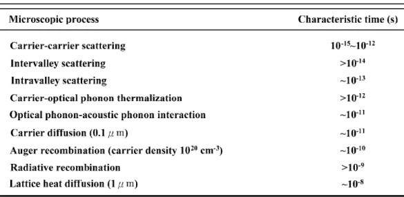
The excitation of semiconductors through equilibrium and the subsequent relaxation processes with different rates has become important in semiconductor field. Fig. 1-1 shows that when the photon energy is larger than the fundamental energy gap, linear absorption occurs. After the optical or electrical excitation of carriers, there are various microscopic processes of momentum and energy relaxation of carriers in the semiconductor such as carrier-carrier scattering, optical phonon scattering, intervalley scattering, etc., that occur in the femtosecond to picosecond time scale. These processes are listed in Table 1-1 and the energy relaxation after excitation is shown in Fig. 1-2. In order to investigate such a short interaction time, femtosecond pump-probe measurements, including differential transmission, reflection, and absorption spectroscopies using ultrashort pulse lasers as the exciting sources, have been widely used for Ⅲ-Ⅴ semiconductors [21][22].
In this thesis, we have investigated the processes such as carrier thermalization, bandgap renormalization, and energy relaxation on bulk GaAs-based materials at room temperature. There will be many benefits to realize the relaxation mechanisms of carriers in materials for manufacturing high-speed photonic devices. Furthermore, bulk GaAs-based materials which emit fluorescence at 1.2-1.5 µm have a lot of potential in long wavelength band.
Fig. 1-1 The electron-hole pair creation following excitation of a semiconductor
with laser radiation of energyhω0.
Energy relaxation follows via optical phonon emission(hωph).
Fig. 1-2 The block diagram illustrating the follow of energy in a photoexcited
semiconductor.
Table 1-1 Fundamental processes in semiconductors.
1-3 Femtosecond
Pump-Probe
Technique
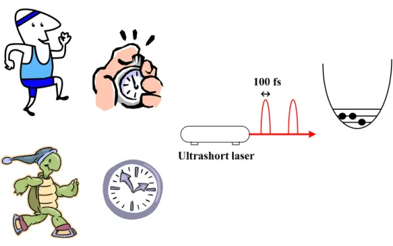
Imagine if we want to measure the speed of a running turtle, we only need a minute-resolution clock. But for measuring the speed of a running man, a second-resolution stopwatch may be required. Different time-scale measurements require different time-resolution tools as shown in Figure 1-3. The femtosecond- resolution pump-probe technique with ultrashort pulse laser can achieve the goal of measuring electron lifetime between various energy bands. In this technique, a femtosecond laser pulse is separated into two beams, a pump and a probe beam, with optical time delay between them. The pump beam should cover the probe beam completely and they overlap spatially on the sample under investigation. After pump beam exciting the samples, there will be a change of absorption coefficient on them. The probe beam is for detecting these changes. The time evolution of the excited states is prospected by varying the time delay. Although we adjust the phase of pump and probe beams perpendicular to each other, coherent artifact which is due to an additional coupling between the two beams is still unavoidable over the region near zero time delay where they interact coherently.
Fig. 1-3 Illustrating different time-scale measurements require different
time-resolution tools.
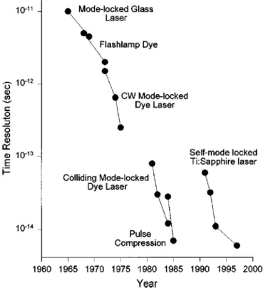
Fig. 1-4 exhibits the technology of generating and detecting short pulses in the pasts few decades. The width of optical pulses has fallen by more than three orders of magnitude since 1966. Fork and Shank developed the colliding pulse mode-locked (CPM) laser in 1981 [23], which made the femtosecond resolution measurement of semiconductors possible.
Fig. 1-4 Schematic diagram of the shortest pulses reported versus years. (Ref. 12)
1-4 Aim of this thesis
In this thesis, we study the ultrafast time-resolved photoreflectance of In0.4Ga0.6As1-xNx/GaAs single quantum wells. We compare the pump-probe
measurements in samples differing in the nitrogen incorporation (x = 0% and 2%) and in the laser wavelengths (λ= 820 nm andλ= 880 nm). At λ= 880 nm, it can prevent the absorption of confining layer GaAs whose bandgap is about 870 nm.
Chapter 2 presents the background concepts and theorems of the ultrafast
spectroscopy of semiconductors. Section 2-1 introduces the scattering processes and carrier relaxation regimes in semiconductors. Then we focus on the reasons of changing in refractive index which includes band filling effect, bandgap renormalization and free carrier absorption.
time-resolved measurement. Chapter 4 shows the results and analysis of our measurements. We have discovered large different phenomena with pumping wavelength at 820 and 880 nm. The change of reflection is negative and positive, respectively. Finally, the perspectives are discussed in Chapter 5.
Chapter 2 Ultrafast Spectroscopy of Semiconductors
2-1 Background Concepts
2-1.1 Carrier Relaxation Regimes
After an ultrashort pulse is sent into a semiconductor, it will be excited to higher energy level and then undergoes several stages of relaxation before it returns back to thermodynamic equilibrium [24]. There are four temporally overlapping regimes of the carrier relaxation:
(a) Coherent Regime
When a semiconductor is excited by an ultrashort pulse, the excitation in the
semiconductor will have well-defined phase relationship within itself and with the electromagnetic field which created the excitations. The excitation can be either real or virtual. The scattering processes in semiconductors that destroy the coherence are exceedingly fast that requires pico- and femtosecond techniques to study. Coherent regime exhibits a lot of fascinating phenomena with basic quantum mechanics in semiconductors.
(b) Non-thermal Regime
In this regime, the excitation is real. After dephasing free electron-hole pairs and
excitons in the coherent regime, the distribution of excitation (i.e. free electron-hole pairs or excitons) is likely to be non-thermal. It means the distribution function can not be represented by a temperature. This regime includes various processes such as carrier-carrier scattering or exciton-exciton scattering. Through the scatterings
above, it takes the non-thermal distribution to a hot, thermalized distribution.
(c) Hot-Carrier Regime
Energy redistribution within the carrier or exciton system is due to carrier-carrier or
exciton-exciton scattering. The procedure leads to a thermalized distribution function of carriers or excitons which can be expressed by a temperature. The temperature is often higher than the lattice temperature, and might be different for various sub-systems. The times of thermalization depend on many factors, for example, carrier density. The electrons and holes thermalize among themselves in hundreds of femtoseconds, while they achieve an ordinary temperature in a few picoseconds. Those thermalized electron-hole pairs take hundreds of picoseconds to reach lattice temperatures, and this process is under interaction with several kinds of phonons in the semiconductor.
Investigation of this regime concentrates on the rate of cooling of carriers to the lattice temperature and the various scattering processes.
(d) Isothermal Regime
All the carriers, phonons, and excitons relax to equilibrium with one another at the
end of hot-carrier regime. Yet there are still some electrons and holes exceeding the thermodynamic equilibrium. In isothermal regime, these excess electron-hole pairs or excitons recombine one another radiatively or non-radiatively then return the semiconductor to the thermodynamic equilibrium.
The schematic diagram of these four regimes is illustrated in Figure 2-1. The
the excitation, the density of excitation, and the lattice temperature…etc.
We should emphasize that many of the physical relaxation in the different regimes are occurring simultaneously and the four relaxation regimes is used for convenience to describe the dynamics of carrier relaxation. For instance, the processes that destroy coherence perhaps also contribute to thermalization of carrier distribution functions, and emission of phonons may take place while the electrons and holes are thermalizing to a hot distribution. The non-thermal carrier distribution function created by an ultrashort pulse is affected by the dephasing of coherent polarization during the pulse. Figure 2-1 is the relaxation regimes under different time scales.
Coherent Regime (≦200fs) ◆ Momentum scattering ◆ Carrier-carrier scattering ◆ Intervally scattering (Γ→L, X ) ◆ Hole-optical-phonon scattering Non-thermal Regime (≦2ps) ◆ Electron-hole scattering ◆ Electron-optical-phonon scattering ◆ Intervally scattering (L, X →Γ) ◆ Carrier capture in quantum wells ◆ Intersubband scattering (ΔE >h ωLO)
Hot-excitation Regime (~1-100ps)
◆ Hot-carrier-phonon interactions ◆ Decay of optical phonons
◆ Carrier-acousitc-phonon scattering ◆ Intersubband scattering (ΔE <h ωLO)
Isothermal Regime (≧100ps)
◆ Carrier recombination
Fig. 2-1 Four temporally overlapping relaxation regimes in photoexcited
2-1.2 Scattering Processes in Semiconductors
There are various kinds of scattering mechanisms. The interactions of electrons, holes, excitons, and phonons will result in different relaxation times in a semiconductor. We will briefly discuss several scattering mechanisms in the following subsections [24].
(a) Carrier-Phonon Interactions
Interaction among carriers and phonons plays an important role in the exchange of energy and momentum between the lattice and carriers, and then determines the relaxation procedure of photoexcited semiconductors. Optical phonon and intervally scatterings proceed in a picosecond time scale, and they are the most frequent events in carrier-phonon interaction. On the contrary, acoustic phonon scattering occurs in a nanosecond time scale and is much less often.
(b) Carrier-Carrier Scattering
Carrier-carrier scattering is accountable for the thermalization of photoexcited non-thermal carriers. The process is judged by Coulomb interaction. It mainly determines the exchange of energy between carriers, and it contains electron-electron, hole-hole, and electron-hole scattering.
(c) Hot Phonons
When a laser beam is incident into a material, the density of photoexcitation will be
moderate to high, and a lot of phonons may be generated as the carriers relax by the emission of phonons. The optical phonons near the zone center have a low
unlikely to leave the photoexcited volume. In this case, the decay time is found to be several picoseconds that a large non-equilibrium phonon population (hot phonons) is created at moderate to high photoexcitation density.
Other scattering processes specific to quantum wells are also significant, such as inter-subband scattering, capture of carriers from the barriers into wells, and real space transfer of carriers from quantum wells into the barriers. These are not the primary processes in our experiments, so we will not put emphasis on them in this article
2-2 Carrier-Induced Change in Refractive Index
2-2.1 Band Filling
According to Pauli exclusive principle, electrons and holes as Fermions can only
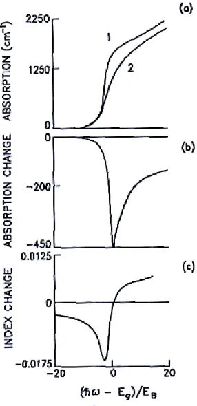
occupy each quantum state once. Therefore with a spin-up and a spin-down carrier, each k state in a semiconductor band can be occupied twice. The carriers in quasi-equilibrium occupy the energetically lowest state first due to the principle of energy minimization. Finally, the states in the bottom of the conduction band will be filled with electrons and in the top of the valence band will be filled with holes. When pumping energy is above the bandgap, carriers will be excited toward higher states and the absorption coefficient α will decrease. Figure 2-2 is a schematic of the bandfilling process [25].
Fig. 2-2 Bandfilling nonlinearity in a narrow-gap semiconductor.
(a) The absorption spectra at low temperatures for low (curve 1) and high (curve 2) carrier densities. (b) The change in the absorption coefficient, ∆α. (c) The
change in the refractive index, ∆n(ω).
The Fermi functions for the electrons (fe) and holes (fh) can only vary between 0
and 1. If we denote energy in the valence band by Ev and in the conduction band by
Ec, then the absorption coefficient of an injected semiconductor is
α(N,P,E) =αo(E) [fv(Ev) - fc(Ec)],
no injection which is given by the square-root law: o( )E C E E E Eg, g E
α = − ≥ , fv is the
probability of an electron occupying a valence band state, and fc is the probability of a
hole occupying a conduction band state. N and P are the concentrations of free electrons and holes, respectively. Band filling results in a change of the absorption coefficient∆α( , , )N P E =αo( )[ ( )E f Ev v − f Ec( )c −1 . Near the conduction and valence ] band edges, we know that fc > 0 and fv < 1 with carrier injection. This equation leads to
a negative change of absorption coefficient, which means the band filling effect decreases α at a fixed incident photon energy.
The real and imaginary parts of the refractive index n-iκare related to each other by Kramers-Kronig (KK) integrals: ( ) ( ') ' ' c E n E dE e E E α ∞ = + −
∫
h 2 2 2 0 2 1 P , where c is thespeed of light, e is the electron charge, α πκ
λ
= 4 , E is the photon energy, and P stands for the principle value of the integral. We define the change of refractive index as Δn (N,P,E) = n(N,P,E) - no(E), where no is the refractive index in the
material with no injection. We can get the change of refractive index from the formula above: ( , , ) ( , , ') ' ' ' c N P E n N P E dE e E E α ∞∆ ∆ = −
∫
h 2 2 0 2P . Carrier injection results in
∆α, and ∆α leads to ∆n. After calculation, the refractive index increases at energies above Eg and vise versa.
2-2.2 Bandgap Renormalization
Fermions with parallel spin can not sit in the same unit cell. Since this situation
would occur for a random distribution, but does not for fermions, we can conclude that the exchange energy increases the average distance between electrons with
parallel spin and consequently reduces their total repulsive Coulomb energy. The reduction of a repulsive energy term means a lowering of the total energy of the electron system.
The correlation energy describes that the electron-hole pair system can lower its energy, if the distribution of electrons and holes relative to each other is not random. The change of Coulomb force leads to a change of atom’s potential, and then a change of band gap.
Wolff first derived the expression for the band gap renormalization:
/ ( )( eh) g o s n e E πε ε π ∆ = − 3 1 3
2 , where εo and εs are the dielectric constants in free space and in the semiconductor, respectively, and neh is the concentration of free electrons or
holes. After carrier excitation, ∆neh results in ∆Eg.
Bandgap reduction causes a red shift of the continuum absorption in semiconductors: (n Eeh, ) C E Eg E ng( eh) C E Eg
E E
α
∆ = − − ∆ − − . It predicts that
∆α is always positive. The nearer to the bandgap, the more rapid decreasing of ∆α. The change of refractive index is also calculated by applying the KK integrals. Due to bandgap renormalization, the largest change of refractive index is near the bandgap and it leads to a negative change of n at energies above the bandgap.
2-2.3 Free-Carrier Absorption
We have mentioned the changes of absorption coefficient and refractive index due to band filling and bandgap renormalization effects. Furthermore, in Drude model, a free carrier in the interband can absorb a photon and move to a higher energy state. The free carrier absorption is also called plasma effect. The change of refractive
index is )( ) 8 ( 2222 h e o m P m N n c e n=− + ∆ ε π λ
, whereλis the photon wavelength, me and mh
are the effective mass of electrons and holes, respectively. Free-carrier absorption causes a negative change of refractive index n.
We have introduced the concepts of carrier dynamics and the background of refractive index change. To find out the ultrafast behavior of InGaAs1-xNx SQW, the
experimental setup of time-resolved photoreflectance will be demonstrated in the following chapter.
Chapter 3 Experiments
3-1 Principle of Femtosecond Time-Resolved Measurement
Ultrashort pulse laser has become a useful tool to investigate ultrafast carrier dynamics. The pulse-width of the laser can achieve femtoseconds (10-15 sec) and it is short enough to measure scattering/relaxation processes in materials.
When a short pulse is incident into the surface of a semiconductor, electrons will transit from valence band to conduction band then relax back to valence band through various relaxation regimes and processes, e.g., carrier-carrier or carrier-phonon scattering as described in Chapter 2. The process of relaxation changes dielectric constant (ε) in the material, and then affects its absorption/reflection rate. From the Fermi’s golden rule, the change of reflection rate is proportional to the number of carriers. The carrier density is estimated using the simple relation: n
n R R ∆ − = ∆ 1 4 2
with the change of refractive index from the Drude model, where
o
m nw Ne
n=− 2/2 2 *ε
∆ , n is the refractive index of sample, N is carrier density, e is elementary charge, m* is the effective mass of the conducting electrons, andεo is the
permittivity of free space. Through a weaker (probe) pulse laser detecting the reflection/transmission continuously, we can understand the phenomenon of carrier dynamics.
The most common technique is pump-probe reflection/transmission measurement. The spot size of the probe beam on the sample is smaller than that of the pump to ensure measuring a uniform photoexcited region. We control the optical path length of pump beam to reach the goal of temporal analysis.
the dotted line represents the temporal change of reflection/transmission rate of the sample after absorbing the pump pulses, and then the probe pulses incidence onto the sample in a delay time t to probe the signal of reflection/transmission. The third part of the figure is the voltage signal transferred from a detector modulated with a chopper. Io(t) is the DC value which represents the intensity of reflection rate R;
∆I(t) is the AC value which represents the change of reflection ∆R. If dividing ∆I(t) by Io(t), we can get a dimensionless signal of ΔR/R. Continuously controlling the
time delay t, we will fully measure the temporal change of ∆R/R.
In addition, if the relaxation time of carriers is longer than the time between two laser pulses, we will not be able to observe the complete relaxation. For example, the repetition rate of the laser is 75 MHz, there are 13.3 nanoseconds (ns) between two laser pulses. Suppose the relaxation time of the sample is longer than 13.3 ns, then the sample will absorb the energy of another pulse before it relaxes. The sample we used has no such a situation.
t (delay)
Pump pulses
Probe pulses
N (t)
time
time
time
13 ns
open I0 (t) Optical chopper @ 3000 Hz at pump pulses ∆I (t)detecter & lock-in amplifier @ 3000 Hz ∆
Reflective probe
pulses
∆ I(t) / I0(t) = R(t) / R0(t)3-2
Experimental System of Femtosecond
Time
-Re
solved Measurement
3-2.1 Ultrafast Laser System
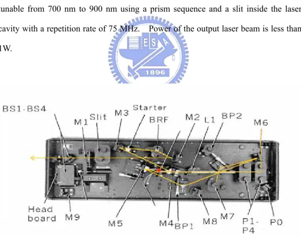
A commercial Kerr-lens-mode-locked Ti:Sappire laser (Coherent Mira900) is used as the light source which is pumped by a diode-pumped frequency-doubled Nd:YVO4
laser (Coherent Verdi-8) with 527 nm with maximum power of about 8W. The structure of Ti:Sappire laser is showed in Figure 3-2. The output wavelength is tunable from 700 nm to 900 nm using a prism sequence and a slit inside the laser cavity with a repetition rate of 75 MHz. Power of the output laser beam is less than 1W.
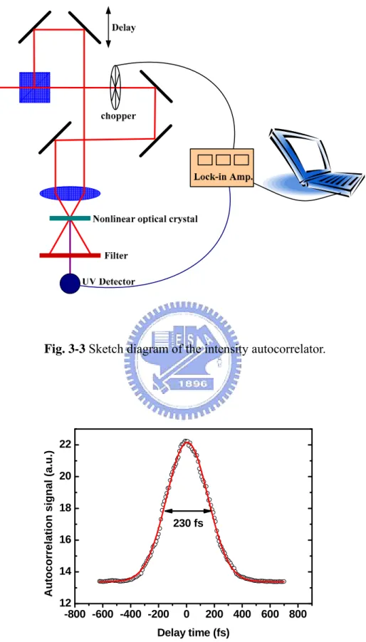
3-2.2 Autocorrelator
An autocorrelation system is for measuring the pulse-width of an ultrafast laser. A
schematic of intensity autocorrelator is showed in Figure 3-3. A beamsplitter separates the laser beam into two beams, and one of them is temporally delayed by a translation stage. We put a beta barium borate (BBO) nonlinear optical crystal at the overlapped focal point of these two beams. The autocorrelation signal comes from second harmonic generation (SHG) of BBO is detected by a silicon detector. The detector receives the frequency-doubled intensity of two laser beams which is determined by autocorrelation function:
dt t I t I S(
τ
)∝∫ ( )× ( −τ
) ,where τ is the time delay, and I(t) is the instantaneous intensity.
Figure 3-4 shows the intensity of measurement [31]. The pulse-width is 230fs obtained by Guassian fitting.
Fig. 3-3 Sketch diagram of the intensity autocorrelator. -800 -600 -400 -200 0 200 400 600 800 12 14 16 18 20 22 Autocorrelatio n sign al (a. u .) Delay time (fs) 230 fs
3-2.3 Experimental Setup of Pump-probe Measurement
The schematic diagram of pump-probe setup performed at room temperature is
shown in Figure 3-5. The mode-locked Ti:Sappire laser described in Section 3-2.1 is the light source. After a variable neutral density filter (ND1) which is for attenuating the power of the laser beam, a 50/50 beamsplitter (BS) splits the beam into pump and probe beams. Another variable neutral density filter (ND2) is used to attenuate the power of probe beam and keep the pump probe ratio 160:1.
A chopper with 25 KHz is used to control pump beam and modulate its frequency for Lock-in Amplifier receiving the signal. A time delay stage with 1.25 µm resolution is applied to change the optical path length of pump beam, resulting in a relative time delay between pump and probe pulses. A half-wave (λ/2) plate rotating the polarization of probe beam by 90o is for avoiding the optical coherent artifacts.
Pump and probe beams meet each other on the sample. Each of them focuses separately by two convex lenses with focal lengths of 10 and 5 cm. The spot size of focused pump beam is about 300 µm. A CCD camera is adopted to ensure the spatial overlap of pump and probe beams. A silicon photodiode detector (HAMAMATSU C5460)is for receiving the reflected light of probe beam and passing it to the lock-in amplifier (Stanford Research System, Model SR830). The final data as a function of temporal delay of pump and probe beams is then showed on a PC monitor.
λ
Fig. 3-5 Femtosecond time-resolved photoreflectance measurement system.
3-3
Zero Delay Point of the System
To find the zero delay point of pump and probe beams is a very important step in this experiment. We focused the two beams respectively on a BBO crystal, and then observed frequency-doubled light after the overlapping point. The position of time delay stage where BBO has the strongest intensity is defined to be zero delay point. Type-Ι phase matching condition of SHG is given by ∆k =k(ω2)−2k(ω1)=0, where 1 1 1 1 ) ( 2 ) ( λ ω π ω n k = , 2 2 2 2 ) ( 2 ) ( λ ω π ω n k = , λ1 =2λ2 , and 2 / 1 2 2 2 2 2 2 2 2 2 ) ) ( sin ) ( cos ( ) , ( ) ( = = + − ω θ ω θ θ ω ω e o e n n n
n , respectively. Here θ is the phase
ordinary refractive index, and ne is the extra-ordinary refractive index.
3-4
InGaAsN Single Quantum Well Structures
The samples we used in our measurement are InGaAs(N)/GaAs single quantum wells which were grown by Tansu et al.. Several dilute-nitride In0.4Ga0.6As single
quantum wells on GaAs substrate were developed by low-pressure metal-organic chemical vapor deposition (LP-MOCVD) method during the past few years. Trimethylgallium, trimenthylaluminium, and trimethylindium are used as group-Ⅲ sources. AsH3 and PH3 are used as group-Ⅴ precursor and U-dimethylhydrazine is
N precursor. The doping sources are SiH4 and dielthylzine for n and p dopants,
respectively. The active layers are 60Å In0.4Ga0.6As1-xNx QW, sandwiched with
various barrier materials: 3000 Å in GaAs cofining layers, 75 Å in GaAs0.85P0.15
tensile barriers, and 30 Å in GaAs0.67P0.33 buffer layers. In and N contents of the
InGaAsN material were determined from high-resolution x-ray diffraction and secondary mass ion spectroscopy. The N composition x in the structures are 0% and 2%, respectively. Figure 3-6 is the schematic diagram of the samples. The growing details of InGaAs(N) can be consulted in Refs. [26][27].
Fig. 3-6 Cross-sectional schematic conduction band diagram of the In0.4Ga0.6As1-xNx
SQW (Ref. [26]).
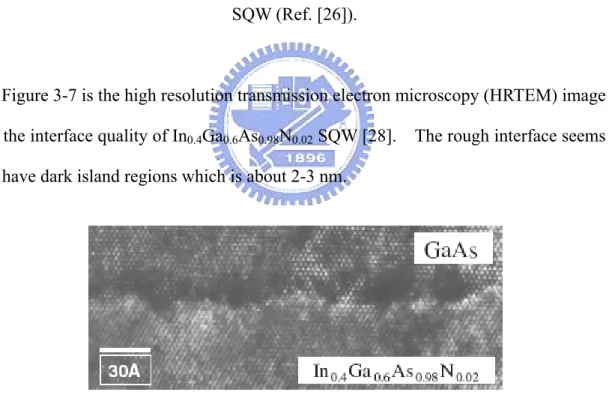
Figure 3-7 is the high resolution transmission electron microscopy (HRTEM) image of the interface quality of In0.4Ga0.6As0.98N0.02 SQW [28]. The rough interface seems
to have dark island regions which is about 2-3 nm.
Fig. 3-7 HRTEM image of In0.4Ga0.6As0.995N0.005/GaAs SQW.
3-5
Method and Steps of Pump-probe Measurement
After setting up the experimental system, the steps of the experiment are as follows:
then adjust it to mode-locking. Use the spectrometer to observe the spectrum of laser beam and ensure the stability of it.
2. Stick the sample on: Obstruct the laser beam before sticking on the sample to
prevent reflected light will be incident back into the laser cavity. Then stick the sample on a three-dimensional stage.
3. Measure the spectrum at room temperature: Ensure the overlapping of pump
and probe beams hourly during the measurement. Control the polarization of pump and probe beams perpendicular to each other to avoid interference. Measure ΔR under different pumping powers.
Chapter 4 Results and Discussion
The pump pulses generate carriers through interband transition in semiconductors can be probed by the time-resolved photoreflectance. After pumping, the various carrier relaxation and decay mechanisms inside semiconductors cause the change of complex refractive index. This brings about the change in reflectivity of probe beam. So from detecting the intensity change of the reflected probe beam, we can get the status of carrier decaying. The reflectivity change can be modeled by the absorption change due to band filling (BF) effect, band gap renormalization (BGR), plasma screening effect, enhancement of absorption, and interband absorption of photons by free carriers (FCA).
The change of reflectivity (ΔR) is because of the change of complex refractive
index (n + iκ). The major contribution to the change of n + iκis written as
Δn =ΔnBF+BGR +ΔnFCA. ΔR is the difference between the reflectivity R with and
without pumping, which is calculated as ΔR(hν) = R(n’,κ’;hν) – R(n,κ;hν). The reflectivity R is given by ) ( 1] ) [n( ) ( 1] -) [n( ) ; R(n, 2 2 2 2 ν κ ν ν κ ν ν κ h h h h h + + + = , where κ is related to
the absorption coefficient by ( ) 4 ) ( α ν π λ ν κ h = h , ( ) 4 ) ( α ν π λ ν κ h = ∆ h ∆ , and n’
and κ’ are the modified real and imaginary parts of refractive index with pumping (under the presence of the carrier density N), respectively.
We have measured InGaAs1-xNx SQWs with x = 0 and 0.02 at 820 and 880 nm,
separately. Since the band gap energy of the GaAs confining layer corresponds to the wavelength of 870 nm, tuning the pumping photon wavelength to 880 nm is enough to avoid absorption of the GaAs confining layer. The bandgap of In0.4Ga0.6As and In0.4Ga0.6As0.98N0.02 SQW are 1.2 µm and 1.45 µm, respectively.
decreases immediately in photon wavelength from 870 to 1000 nm, and its value at 870 nm is far more than that at 880 nm [29]. We have reduced the absorption of GaAs effectively when tuning the pumping wavelength to 880 nm. The definition of penetration depth is the reciprocal of absorption coefficient. From Figure 4-1, we can extract the penetration depth of GaAs at 800 and 880 nm. They are 1.43 µm and 1000 µm, respectively. As we know, the thickness of confining layer GaAs is 0.3 µm, so the intensity of the laser beam which is incident into the quantum well remains 0.81Io at 800 nm and 0.9997Io at 880nm, where Io is the incident intensity of the beam.
Therefore, the single quantum well can efficiently absorb the pumping laser beam. Notice that the exciton resonances are very weak in bulk GaAs and thus can only be observed at very low temperature [30].
Fig. 4-1 Absorption curve of GaAs (Ref. [29]).
We extract the data from 10 to 50 mW and obstruct the laser beam between every measuring to reduce the thermal effect. Therefore, the thermal effect is not
4-1 Ultrafast
Time-Resolved Photoreflectance of
In
0.4Ga
0.6As
1-xN
xSQW
In order to describe a complete sketch of the optical properties of In0.4Ga0.6As1-xNx, we review some results of Y. H. Lin in 2005 [31]. Keeping the
pumping wavelength at 800 or 820 nm, whose corresponding energies are both above the bandgap of GaAs, Figure 4-2 shows the results of time-resolved photoreflectance of bulk GaAs and In0.4Ga0.6As1-xNx (x = 0 and 0.02) SQW with pumping power
varying from 10 to 100 mW, respectively. The fast rising and decaying responses in Figure 4-2(a), (b), and (c) are because the generation of carriers occupies the optical-coupled transition states. After the absorption, the carriers scatter out of their initial states and subsequent relax toward the band edges through carrier-carrier and carrier-phonon scattering. In bulk GaAs, there is a positive ∆R/R, however, In0.4Ga0.6As1-xNx SQWs have the opposite behavior with GaAs with negative ∆R/R.
It is amazing to find that the thickness of these quantum wells is only 60 Å, we still can distinguish the huge differences of carrier dynamics between bulk GaAs and In0.4Ga0.6As1-xNx SQWs. The positive ∆R so as positive index change is mainly due
to band filling effect because the pumping photon energy is above the bandgap of bulk GaAs. On the other hand, the negative change of transient reflectance of In0.4Ga0.6As1-xNx SQWs corresponds to a negative index change. The exact
mechanism of negative index change is very complicated and still not fully understood. Because the thickness of these quantum wells is only 60 Å and the pumping photon energy is above the bandgap of the GaAs confining layer, we speculate that the carriers are mainly excited in the confining layer then quickly trapped into the quantum wells of both InGaAs and InGaAsN SQW samples. Due to
the much smaller bandgap, the band filling would not contribute to index change that results in negative change of transient reflectance from the band gap renormalization and the free-carrier absorption (FCA) or re-excitation of trapped carriers into the conduction band [32]. 0 2000 4000 6000 8000 0.000 0.001 0.002 0.003 0.004 0.005 0.006 0.007 0.008 0.009 0.010 0.011 ∆ R/R Time delay (fs) 100mW 90 mW 80 mW 70 mW 60 mW 50 mW 40 mW 30 mW 20 mW 10 mW
(a) bulk GaAs
0 2000 4000 6000 8000 10000 -0.006 -0.005 -0.004 -0.003 -0.002 -0.001 0.000 ∆ R/R Time delay (fs) 10 mW 20 mW 30 mW 40 mW 50 mW (b) In0.4Ga0.6As SQW
-2500 0 2500 5000 7500 10000 12500 -0.0010 -0.0008 -0.0006 -0.0004 -0.0002 0.0000 40mW 20mW 30mW 50mW ∆ R/ R Time delay (fs) 10mW (c) In 0.4Ga0.6As0.98N0.02 SQW
Fig. 4-2 The pump-intensity dependent time-resolved photoreflectance of
(a) bulk GaAs, (b) In0.4Ga0.6As SQW pumped at 800 nm from [31], and (c)
In0.4Ga0.6As0.98N0.02 SQW pumped at 820 nm.
Although the mechanism of carrier relaxation in In0.4Ga0.6As1-xNx SQWs is
distinct from that in bulk GaAs, the GaAs confining layer whose bandgap is 870 nm makes the carrier relaxation complicated when pumping wavelength is at 800 or 820 nm. It can truly avoid the absorption of GaAs confining layer by adjusting the pumping wavelength to 880 nm. Shown in Figure 4-3 are the results of time-resolved photoreflectance of In0.4Ga0.6As1-xNx (x = 0 and 0.02) SQWs with
pumping power varying from 10 to 60 mW at 880 nm. It reveals a contrary result comparing to the previous measured results in Figure 4-2. The measured reflectance turned to be positive at 880 nm. The positive change of transient reflectance is due to the band filling effect, indicating a positive change of refractive index (∆n > 0) [24]. The opposite phenomenon may result from different initial occupied states of the photo-excited carriers for two pump wavelengths. With pumping wavelength < 820 nm, the carriers are generated in confining layer GaAs during pumping, and then the
quantum well capture those carriers in a short time. After carriers are trapped in In0.4Ga0.6As1-xNx SQWs, there will be no band filling effect but the increase of carriers
in the well could cause bandgap shirinkage and therefore leads to negative index change so as the negative ∆R.
Locations of the peaks in Figure 4-3(a) are a little different with various pumping power, the reason might be fluctuation of our laser or vibration of the step-motor. Besides, we have adjusted the polarization of pumped and probe beam perpendicular to each other, the interference caused by overlapping of pumped and probe beam occurs around the zero delay point which is clearly seen in Figure 4-3(b). We extract every peak at different pumping power and sketch them in Figure 4-4 to expose the tendency.
-2000 0 2000 4000 6000 8000 -0.0003 0.0000 0.0003 0.0006 0.0009 0.0012 (a) In0.4Ga0.6As SQW 20mW 30mW 40mW 50mW60mW ∆ R/R Time delay (fs) -2500 0 2500 5000 7500 10000 12500 -0.00005 0.00000 0.00005 0.00010 0.00015 0.00020 0.00025 50mW 20mW 40mW 30mW 10mW ∆ R/R Time delay (fs) (b) In 0.4Ga0.6As0.98N0.02 SQW
Fig. 4-3 The pump-intensity dependent time-resolved photoreflectance of (a)
In0.4Ga0.6As SQW and (b) In0.4Ga0.6As0.98N0.02 SQW pumped at 880 nm.
Due to the interference of pumped and probe beams nearby the zero time delay, it is hard to find the exact location of peaks with pumping wavelength at 880 nm in Figure 4-3(d). By fitting the curves with a Lorentzian and a biexponential function to all of the photoreflectance curves, the measured peak amplitude of ∆R versus pumping
power density of In0.4Ga0.6As SQW is displayed in Figure 4-4. The magnitude of ∆R
peak is proportional to the density of carriers accumulated in the allowed optical transition states after photoexcitation. The carrier density N can be calculated using the relation mentioned in Section 3-1 based on the Drude model: n
n R R ∆ − = ∆ 1 4 2 ,
where ∆n=−Ne2/2nω2m*εo. The estimated carrier densities are listed in Table
4-1.
Due to absorption by the GaAs confining layer, the carrier densities with pumping wavelength < 820 nm are an order of magnitude larger than those of pumped at 880 nm for both samples but the larger carrier density for InGaAs SQW than for InGaAsN SQW. It is worth to note that when pumped at 880 nm, whose photon energy is below GaAs bandgap but above those of both samples, the carrier densities are nearly the same at the lowest pumping; whereas, with increasing pumping power density, the carrier density increases faster than that of InGaAsN SQW.
Table 4-1. List of carrier densities of In0.4Ga0.6As, In0.4Ga0.6As0.98N0.02 with various pumping power. In0.4Ga0.6As In0.4Ga0.6As0.98N0.02 N (1018 cm-3) N (1018 cm-3) Power density (MW/cm2) 800 nm 880 nm 820 nm 880 nm 184.6 6.19 0.11 0.83 0.12 369.2 6.95 0.78 1.31 0.30 553.8 8.87 1.36 1.70 0.39 738.4 10.07 1.82 2.07 0.46 923 11.76 2.12 2.21 0.51 1107.6 -- 2.19 -- --
After being pumped to the higher states, carriers can diffuse in the 3000Å GaAs confining layer or be trapped into the quantum well. The band filling effect will not be obvious, so all of the carrier densities basically linearly increase with the pumping power for those pumping at wavelength < 820 nm in Figures 4-4(a) and (b). On the other hand, when pumping at 880 nm, carriers will localize in InGaAs1-xNx single
quantum well. The band filling effect dominates positive ∆n and it will saturate at high pumping, that is because ∆α is nonlinear, the relation of power density versus peak amplitude in Figure 4-4(c) and (d) is also nonlinear.
200 400 600 800 1000 2.5 3.0 3.5 4.0 4.5 5.0 5.5 6.0 power density (MW/cm2) P eak am plit ude ( 10 -3 ) (a) InGaAs SQW at 800nm 200 400 600 800 1000 0.3 0.4 0.5 0.6 0.7 0.8 0.9 Power density (MW/cm2) - Peak amplitud e
(
10 -3)
(b) InGaAsN SQW at 820nm200 400 600 800 1000 1200 -0.2 0.0 0.2 0.4 0.6 0.8 1.0 1.2 1.4 Power density (MW/cm2) P e ak am pl it ud e ( 10 -3 ) (c) InGaAs SQW at 880nm 200 400 600 800 1000 0.04 0.08 0.12 0.16 0.20 0.24 Power density
(
MW/cm2)
Peak am plitude(
10 -3)
(d) InGaAsN SQW at 880nmFig. 4-4 The measured ∆R peak amplitude versus pumping power with pumping
wavelength at 800/820 nm in (a) In0.4Ga0.6As (b) In0.4Ga0.6As0.98N0.02 SQW and at 880
4-2 Carrier Relaxation Time of InGaAs
1-xN
xSQW
We extract the relaxation time of carriers by fitting the experimental ∆R traces by using a double exponential decay function, A exp(-t/τ1) + B exp(-t/τ2). We obtain the
carrier decay time which is exhibited in Figure 4-5. The profile shows an initial fast decay followed by a slower relaxation [33]. The fast component of carrier lifetime approximates 2-3 ps with pumping wavelength at 800 nm and 1-2.5 ps at 880 nm. It does not change much with increasing pumping power. It is attributed to the carrier-carrier scattering. Because the pumping energy remains still, the rate of carrier-carrier scattering will basically not change even if the pumping power is already different. The later component of relaxation time is about several tens ps with pumping wavelength at 800 nm and 2-8 ps at 880 nm. As we know, τ2
increases with increasing pumping power. The reason of these results is the appearance of hot phonons [24]. After receiving the energy from pumping beam, the carriers transfer their additional kinetic energy to phonons. Those phonons become hot phonons, and then transfer the energy back to carriers. Carriers which have more kinetic energy also take more time to relax to thermalization. As a result, it takes longer to decay when pumping power is rising. On the other hand, we could not judge the trend in Figure 4-5(a) due to the lack of statistics.
300 450 600 750 900 0 1 2 3 4 5 0 4 8 12 16 20 τ 2 (ps) Power Density (MW/cm2) τ 1 (ps ) (a) 800nm 400 600 800 1000 1200 0 2 4 6 8 0 2 4 6 8 10 τ 2 (p s ) Power density (MW/cm2) τ1 (p s) (b) 880nm
Fig. 4-5 The carrier lifetime versus pumping power in In0.4Ga0.6As SQW with pump
wavelength at (a) 800 (b) 880 nm.
Figure 4-6 presents the carrier relaxation time fitted from Figure 4-3, and the illustrations represent In0.4Ga0.6As0.98N0.02 SQW with the pumping wavelength at 820
and 880nm, respectively. In In0.4Ga0.6As0.98N0.02 SQW, the photo-excited carrier
N-incorporation during or after they experienced electron-hole scattering to lose their excess kinetic energy. In Figure 4-6(a), the observed short relaxation time of ~1-2 ps is attributed to the carrier-carrier scattering; τ1 is almost constant for various power
densities. The longer decay time of 5-8 ps increases with the pumping power that is attributed to hot phonon decay. The mechanism of hot phonon has already reported in Section 4-1. After adjusting the pumping wavelength to 880 nm, we discover that the behavior of τ2 is contrary to the second decay time at 820nm. Originally it takes
0.3-0.8 ps to relax in Figure 4-6(b), carrier-carrier scattering occurs at this moment. Then it takes 2-4.5 ps to accomplish the later relaxation process, which decreases when the pumping power increases. As we know, the sample has lasing characteristics [34], stimulated emission decay times faster than 10 ps have been noticed. The stronger of the pumping intensity, the more carriers will be in the upper state, and then the carrier decaying will also be faster [35]. Moreover, we can only see an exponential decay time with pump power in 10mW through large fluctuation at low pumping.
200 400 600 800 1000 0 2 4 6 8 0 2 4 6 8 10 τ 2 ( p s ) τ 1
(
ps)
Power density (MW/cm2) (a) 820nm 200 400 600 800 1000 0.0 0.5 1.0 1.5 2.0 2.5 0 1 2 3 4 5 6 τ 2 (ps) Power density (MW/cm2) τ 1 (ps) (b) 880nmFig. 4-6 The carrier lifetime versus pumping power in In0.4Ga0.6As0.98N0.02 SQW with
pump wavelength at (a) 820 (b) 880 nm.
Comparing In0.4Ga0.6As SQW with In0.4Ga0.6As0.98N0.02 SQW, it clearly reveals that
In0.4Ga0.6As SQW shows not only an order of magnitude ∆R/R larger than that of
In0.4Ga0.6As0.98N0.02 SQW, but also a longer relaxation time. It is consistent with
the time-resolved PL measurements which were done by Lifang et al. [19] and the below threshold modulation frequency response measurements which were studied by
Anton et al. [36]. This phenomenon can be explained by presence of defects after nitrogen incorporation. Some trap states are formed within the bandgap by defects, and they will capture excited carriers efficiently. The trap states act like nonradiative recombination centers. This process lasts a shorter time than the intraband relaxation, and that is why carrier lifetime in In0.4Ga0.6As0.98N0.02 is shorter. Besides,
carriers in excited states above the conduction band minimum can also be trapped due to the localization of these trap states. Furthermore, the carrier density of In0.4Ga0.6As0.98N0.02 SQW is an order of magnitude smaller than that of In0.4Ga0.6As
SQW, which is mainly due to the bandgap of In0.4Ga0.6As0.98N0.02 being farther from
Chapter 5 Conclusion and Perspectives
We have successfully studied the ultrafast time-resolved photoreflectance of InGaAsxN1-x (x = 0 and x = 2%) single quantum wells even with extremely thin
thickness of 60 Å and 3000 Å wide GaAs confining layer. After tuning the pumping wavelength to 880nm, it effectively avoids the absorption of confining layer GaAs. It is interesting to find that the change of refractive index turns to be positive, which is because the band filling effect replaces the renormalization of bandgap.
The calculated carrier densities and estimated relaxation times of carriers are also demonstrated. As mentioned above, the bandgap will be reduced and the carrier dynamics will be very different after nitrogen incorporation. With pumping wavelength at 880nm, the shorter carrier lifetimes of In0.4Ga0.6As and
In0.4Ga0.6As0.98N0.02 SQW are both independent of pumping power, which indicates
the mechanism of carrier-carrier scattering. Nevertheless, the longer lifetime is proportional to the pumping power in In0.4Ga0.6As SQW and inversely proportional to
the pumping power in In0.4Ga0.6As0.98N0.02 SQW. The explanation of this
phenomenon is hot phonon decay for the former and stimulated emission for the later. In addition, carrier lifetime in In0.4Ga0.6As0.98N0.02 SQW is shorter than that in
In0.4Ga0.6As SQW, which is on account of the appearance of the local defect states
during nitrogen doping.
There are still some ways to progress the experimental setup. Replacing the optical chopper by an AOM modulator can improve the signal to noise ratio; using a pair of prisms can compress the pulse width of laser. We will further measure the photoluminescence emission of In0.4Ga0.6As0.98N0.02 under various pumping power to
ensure the behavior of diode laser. Moreover, different material of samples like ZnO thin films can be surveyed in the future.
References
[1] A.Y. Polyakov, N.B. Smirnov, A.V. Govorkov, A.E. Botchkarev, N.N. Nelson, M.M.E. Fahmi, J.A. Griffin, A. Khan, S. Noor Mohammad, D.K. Johnstone, V.T. Bublik, K.D. Chsherbatchev, M.I. Voronova, and V.S. Kasatochkin, Solid-State Electron., 46, 2147(2002)
[2] H. P. Xin, and C. W. Tu, Appl. Phys. Lett., 72, 2442 (1998).
[3] G. L. Belenky, C. L. Reynolds, D. V. Donetsky, G. E. Shtengel, M. S. Hybertsen, M. A. Alam, G. A. Baraff, R. K. Smith, R. F. Kazarinov, J. Winn, and L. E. Smith, IEEE J. Quantum Electron., 35, 1515 (1999).
[4] N. Tansu, N. J. Kirsch, and L. J. Mawst, Appl. Phys. Lett. 81, 2523 (2002). [5] N. Tansu, J. Y. Yeh, and L. J. Maest, Appl. Phys. Lett. 82, 3008 (2003). [6] N. Tansu, J. Y. Yeh, and L. J. Maest, Appl. Phys. Lett. 82, 4038 (2003).
[7] N. T. Hashimoto, Kazuhiko Misawa, and Roy Lang, Appl. Phys. Lett. 82, 2749 (2003)
[8] G. Sucha, S. R. Bolton, D. S. Chemla, D. L. Sivco, and A. Y. Cho, Appl. Phys. Lett., 65, 1486 (1994).
[9] P. Borri, W. Langbein, J. M. Hvam, and F. Martelli, Phys. Rev. B., 59, 2215 (1999).
[10] P. Bhattacharya, S. Ghosh, S. Pradhan, J. Singh, W. zong-Kwei, J. Urayma, K. Kim, and T. B. Norris, IEEE J. Quantum Electronics., 39, 952 (2003).
[11] D.E. Mars, D.I. Babic, Y. Kaneko, and Ying-Lan Chang, J. Vac. Sci. Technol. B,
17, 1272 (1999)
[12] A. Vinattieri, D. Alderighi, M. Zamfirescu, M. Colocci, A. Polimeni, M. Capizzi, D. Gollub, M. Fischer, and A. Forchel, Phys. Stat. Sol. (a), 195, 558 (2003) [13] LiFang Xu, D. Patel, and C.S. Menoni, Appl. Phys. Lett., 89, 171112 (2006)
[14] Lifang Xu, D. Patel, G. Vaschenko, O. Anton, C. S. Menoni, J. Y. Yeh, T. T. V. Roy, L. J. Mawst, N. Tensu, CLEO/QELS ’05, Baltimore, Maryland, USA. [15] R. A. Mair, J. Y. Lin, H. X. Jiang, E. D. Jones, A. A. Allerman, and S. R. Kurtz,
Appl. Phys. Lett. 76, 188 (2000).
[16] A. Kaschner, T. Lüttgert, H. Born, A. Hoffmann, A. Yu. Egorov and H. Riechert, Appl. Phys. Lett. 78, 1391 (2001).
[17] A. Vinattieri, D. Alderighi, M. Zamfirescu, M. Colocci, A. Polimeni, M. Capizzi, D. Gollub, M. Fischer, and A. Forchel, Appl. Phys. Lett. 82, 2805 (2003).
[18] O. Anton, C. S. Menoni, J. Y. Yeh, L. J. Mawst, J. M. Pikal, and N. Tansu, IEEE Photon. Technol. Lett., 17, 953 (2005).
[19] Lifang Xu, D. Patel, G. Vaschenko, O. Anton, C. S. Menoni, J. Y. Yeh, T. T. V. Roy, L. J. Mawst, N. Tensu, CLEO/QELS ’05, Baltimore, Maryland, USA. [20] Andreas Othonos, J. Appl. Phys., 83, 1789 (1998).
[21] D. H. Auston, S. McAfee, C. V. Shank, E. P. Ippen, and O. Teschke, Solid-State Electon., 21, 147 (1978).
[22] W. Z. Lin, R. W. Schoenlein, E. P. Ippen and R. A. Logan, Appl. Phys. Lett., 50, 124 (1987).
[23] R. L. Fork, B. I. Greene, and C. V. Shank, Appl. Phys. Lett., 38, 671 (1981). [24] J. Shah, Ultrafast Spectroscopy of Semiconducters and Semiconductor
Nanostructures, Springer-Verlag, Berlin, (1996).
[25] Nasser Peyghambarian, Stephan W. Koch, Andre Mysyrowicz, Introduction to Semiconductor Optics, (1993)
[26] N. Tansu, N. J. Kirsch, and L. J. Mawst, Appl. Phys. Lett., 81, 2523 (2002). [27] N. Tansu, J. Y. Yeh, and L. J. Maest, Appl. Phys. Lett., 82, 3008 (2003).
[28] H. C. Kuo, F. I. Lai, Y. H. Chang, M. Y. Tsai, S. Y. Kuo, S. C. Wang, N. Tansu, J. Y. Yeh, and L. J. Maest, J. J. Appl. Phys., 44, 6204(2005)
[30] D.S. Chuu and Ying-Chih Lou, Phys. Rev. B, 43, 14 504 (1991)
[31] Ying-Hsiu Lin, The Ultrafast Time Resolved Photoreflectance Measurement of
InGaAsxN1-x Single Quantum Wells, National Chiao Tung University, (2005)
[32] B. R. Bennett, R. A. Soref, and J. A. D. Alamo, IEEE J. Quantum Electronics., 26, 113 (1990).
[33] Clementine Symonds, Juliette Mangeney, Guillaume Saint-Girons, and Isabelle Sagnes, Appl. Phys. Lett., 87, 012107 (2005)
[34] N. Tansu, J. Y. Yeh, and L. J. Mawst, IEEE J. Quantum Electron., 9, 1220 (2003) [35] Umit Ozgur and Henry O. Everitt, Phys. Rev. B, 67, 155308 (2003)
[36] O. Anton, C. S. Menoni, J. Y. Yeh, L. J. Mawst, J. M. Pikal, and N. Tansu, IEEE Photon. Technol. Lett., 17, 953 (2005).