亞東技術學院
資訊與通訊工程研究所
碩士論文
天線輻射對電磁干擾的影響分析
EMI Effect from Antenna Radiation
研 究 生:裴笛翰
指導教授:張道治
誌謝
首先本人為表達最誠摯的感謝給指導教授張道治博士,在碩士學 習過程中,從實驗的進行到期刊論文的發表,老師無私的教導與教誨, 讓我從大學時懵懵懂懂的專題生到研究所的畢業生,老師不僅僅只傳 授專業上的知識,更是我人生的導師,能有今天小小的成就,要感謝 的人太多太多,無論是教導過我的師長或是陪我一路走來的同窗夥伴, 讓我即使遭遇困難與挫折,也能化阻力為助力。因為有你們使我成長, 我永遠都不會忘記這個大家庭所賦予我的點點滴滴,並不是因為人多 而稱作家庭,而是因為有你們才稱之為家庭,正因為有你們才有今天 的我。 感謝曾協助與提供我意見的廖兆祥學長、林志恒學長,以及一起 渡過研究所時光的同窗好友,陳晟瑋同學、顏紹翔同學、陳俊傑同學, 還有通訊中心的詹千慧助理、邱裕中以及女友峰琬的鼓勵與支持,是 我能堅持到最後的重要因素,最後更加感謝讓我衣食無虞,使我無後 顧之憂能專心致力於學業的家人們,不論是在精神上或是行動上的支 持,感謝所有曾幫助過我的老師、朋友及家人,因為有你們讓我的人 生版圖上添加許多色彩,將永銘於心。在此,僅將小小成果獻給所有 鼓勵與關心我的師長朋友及摯愛的家人們。 裴笛翰 謹誌於 亞東技術學院 中華民國 100 年 8 月摘要
在本論文中,分成四部分來做探討:第一部分,先設計應用於 GSM900 MHz、1800 MHz 的 PIFA 天線,模擬及量測分析當人體模型靠 近天線時,對天線特性的影響,第二部分,利用 GEMS 模擬軟體,分 析印刷電路板受鄰近天線輻射引起之電流分佈及產生的電磁干擾問 題,當天線輻射時,對於四周的電子元件產生電磁干擾,將會降低通 訊系統的接收靈敏度;第三部分,量測印刷電路板中電磁干擾之電場 及電流分佈,在傳統量測方式,量測時探棒與待測物距離太近時易產 生耦合效應,距離較遠時,則電場或電流分佈位置之解析度不佳,無 法精確預估受干擾之位置,本論文採用近場量測方式,將量測之近場 參數,轉換成印刷電路板的高解析度電流分佈;在最後一部分,我們 將針對電磁干擾問題加以除錯改良,以減少電磁干擾、耦合效應及解 析度不佳等問題,增加系統之接收靈敏度。 關鍵字:電磁干擾、印刷電路板、PIFAAbstract
This paper will divide four items. The first is design a PIFA antenna for GSM900 and GSM1800, and discussing antenna performance of the human body close to the antenna. Second is using GEMS simulation tool to analyze current distribution and electromagnetic interference of printed circuit board by the antenna. When the antenna radiation, the antenna will produce the electromagnetic interference on the electronic components, it will reduce the receiver sensitivity of communication systems. Third is measurement printed circuit board for electromagnetic interference and electric field or current distribution. In the traditional measurement method, if the near field probe closes the print circuit board, it will cause the mutual coupling problem, If the near field probe is far away from the print circuit board, it will not to get high resolution image, it not easy to discover the location of interference, this thesis will use surface scan method to measure near field parameters, and improve traditional measurement method. Finally is debug electromagnetic interference to reduce electromagnetic interference and mutual coupling problems. It will increase receiver sensitivity of communication systems.
Contents
博碩士論文授權書...I 論文封面...II 論文指導教授推薦書...III 論文口試委員審定書...IV 誌謝...V 中文摘要...VI English Abstract...VII Contents. ...VIII List of Figures...XChapter 1 Introduction
1.1 Introduction...1 1.2 Research motivation...1 1.3 Background... ...4 1.4 Outline of thesis...7Chapter 2 Basic Antenna Theory
2.1 Introduction...112.2 Basic of monopole antenna...11
2.3 Basic of Inverted F ntenna...12
2.4 Basic of meander-line antenna...13
Chapter 3 Design 900/1800 MHz PIFA Antenna on a Mobile
Phone with a Proximate Head
3.1 Introduction...17
3.2 PIFA antenna design...17
3.3 Simulation of PIFA antenna with head model...18
3.4 Simulation and measurement results...19
3.5 Summary...20
Chapter 4 Simulation and Measurement of RE for PCB
4.1 Introduction...404.2 Design and analysis of PIFA antenna for the electric field distribution...40
4.3 Simulation and test results...41
4.4 Summary ...42
Chapter 5 Build High Resolution Circuit Image
5.1 Introduction...495.2 Diffraction field by NF aperture...49
5.3 Simulation and test results...52
5.4 Summary...53
Chapter 6 Conclusion
Conclusion...67List of Figures and Tables
Fig.1.1 Structure of EMI problems from IC……….…8
Fig.1.2 Structure of EMC……….…8
Fig.1.3 Structure of TEM cell……….…..9
Fig.1.4 Structure of Faraday Cage……….….…..9
Fig.1.5 Structure of magnetic probe method……….….….10
Fig.1.6 Structure of surface scan method……….……….….….10
Fig. 2.1 Structure of the dipole and monopole antenna………….…..15
Fig. 2.2 Structure of the inverted F antenna……….……15
Fig. 2.3 Structure of meander-line dipole antenna……….…..16
Fig.3.1 PIFA antenna structure……….…....22
Fig.3.2 Reflection coefficient of dual-band PIFA antenna…….……..22
Fig.3.3 Dual-band PIFA antenna Smith Chart……….….23
Fig.3.4 PIFA antenna efficiency at 900MHz……….…...23
Fig.3.5 PIFA antenna efficiency at 1800MHz...24
Fig.3.6 PIFA antenna gain at 900MHz……….24
Fig.3.7 PIFA antenna gain at 1800MHz………...25
Fig.3.8 PIFA antenna in E-Plane pattern at 900MHz………...25
Fig.3.9 PIFA antenna in H-Plane pattern at 900MHz...26
Fig.3.10 PIFA antenna in E-Plane pattern at 1800MHz………...26
Fig.3.11 PIFA antenna in H-Plane pattern at 1800MHz………..27
Fig. 3.12 Simulation electric field at 900MHz……….27
Fig. 3.13 Simulation surface current at 900MHz……….28
Fig. 3.14 Simulation electric field at 1800MHz………...28
Fig.3.16 Simulation structure………...29 Fig.3.17 Simulation reflection coefficient at different distances…….30 Fig.3.18 Simulation antenna efficiency at 900MHz with different
distances...30 Fig.3.19 Simulation antenna efficiency at 1800MHz with different
distances...31 Fig.3.20 Simulation antenna gain at 900 MHz with different
distances...31 Fig.3.21 Simulation antenna gain at 1800MHz with different
distances...32 Fig.3.22 Simulation 900 MHz E-plane pattern at different
distances...32 Fig.3.23 Simulation 900 MHz H-plane pattern at different
distances...33 Fig.3.24 Simulation 1800 MHz E-plane pattern at different
distances...33 Fig.3.25 Simulation 1800 MHz H-plane pattern at different
distances...34 Fig.3.26 Measurement structure...35 Fig.3.27 Measurement reflection coefficient with different
distances...36 Fig.3.28 Measurement antenna efficiency at 900 MHz with different
distances...37 Fig.3.29 Measurement antenna efficiency at 1800 MHz with different distances...37 Fig.3.30 Measurement antenna gain at 900 MHz with different
distances...38
Fig.3.31 Measurement antenna gain at 1800 MHz with different distances...38
Fig.3.32 Measurement 900 MHz E-plane pattern with different distances...39
Fig.3.33 Measurement 900 MHz H-plane pattern with different distances...39
Fig.3.34 Measurement 1800 MHz E-plane pattern with different distances...40
Fig.3.35 Measurement 1800 MHz H-plane pattern with different distances...40
Fig.4.1. Structure communication system...44
Fig.4.2. Simulated electric current at 900 MHz...44
Fig.4.3. Simulated electric current...45
Fig.4.4. Simulated area...45
Fig.4.5. Simulated surface current density at 900 MHz...46
Fig.4.6. Simulated surface current density at 1800 MHz...46
Fig.4.7. Aperture field scan of antenna...47
Fig.4.8. Simulation and measurement of aperture field at 900MHz....47
Fig.4.9 Simulation and measurement of aperture field at 1800MHz...48
Fig.5.1 the diffraction field by near field aperture...55
Fig.5.2 (a) Plane position and rectangular aperture antenna radiation analysis: x-z plane...55
Fig.5.2 (b) Plane position and rectangular aperture antenna radiation analysis: y-z plane...56 Fig.5.2 (c) Plane position and rectangular aperture antenna radiation
analysis: x -y plane...56
Fig.5.3 Equivalence principle...57
Fig.5.4 Transformation formula structure...57
Fig.5.5 PIFA antenna structure...58
Fig.5.6 Surface current at 900 MHz...58
Fig.5.7 Surface current at 1800 MHz...59
Fig.5.8 Magnetic field at distance 0.3 cm in 900 MHz...59
Fig.5.9 Magnetic field at distance 0.3cm in 1800MHz...60
Fig.5.10 Magnetic field at distance 0.5 cm in 900 MHz...60
Fig.5.11 Magnetic field at distance 0.5 cm in 1800 MHz...61
Fig.5.12 Magnetic field at distance 1 cm in 900 MHz...61
Fig.5.13 Magnetic field at distance 1 cm in 1800 MHz...62
Fig.5.14 Transformation formula structure with different scope...62
Fig. 5.15 Transformed surface current at distance 3mm in 900 MHz...63
Fig. 5.16 Transformed surface current at distance 3mm in 1800 MHz...63
Fig. 5.17 Transformed surface current at distance 3mm in 900 MHz...64
Fig. 5.18 Transformed surface current at distance 3mm in 1800 MHz...64
Fig. 5.19 Transformed surface current at distance 5mm in 900 MHz...65
Fig. 5.20 Transformed surface current at distance 5mm in 1800 MHz...65 Fig. 5.21 Transformed surface current at distance 1cm in 900
MHz...66 Fig. 5.22 Transformed surface current at distance 1cm in 1800
MHz...66
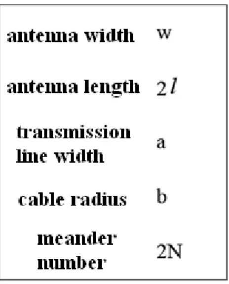
Table 2.1 Structure parameters of meander-line dipole antenna...16 Table 3.1 Simulation antenna efficiency and gain with different
Chapter 1
Introduction
1.1 Introduction
In this thesis, the main purpose is improving receiver sensitivity for the communication system. Preliminary analysis using GEMS software, the analysis of cable and printed circuit board near the antenna radiation to cause the current distribution and human body impact of antenna frequency and efficiency, obvious to see, the distance change of the antenna and device under test (DUT) about the influence of frequency and efficiency. It can be quick and accurate analysis of current distribution of printed circuit boards and electromagnetic interference. For the transmitter source to determine the printed circuit board caused by electromagnetic interference, thereby improving the receiver sensitivity, which will help save development costs and accelerate time to market.
1.2 Research motivation
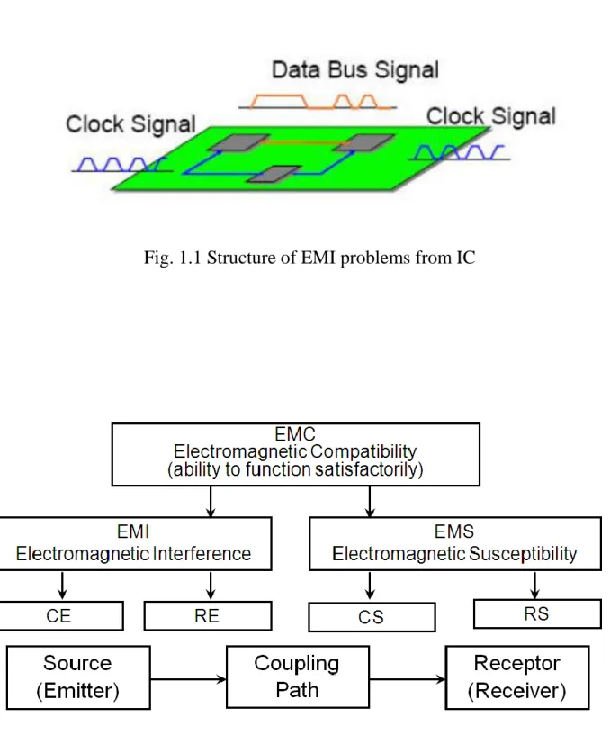
In nowadays the requirements of communication system will include compact size, light weight, and high antenna efficiency. Due to the high effective radiation power, it will induce the strong current density on the print circuit board which is near the antenna. If the high sensitivity receiver is near the strong current density area, it will reduce the receiver sensitivity. Fig.1.1 is
The EMI problems can be divided into two kinds, conduction interference and radiation interference. Conduction interference is referred to mutual coupling between the two circuits through the conductive medium, while the radiation interference is the mutual coupling from another circuit through the space. So the study on EMI problem is that the interference with the source, coupling path and receive. Fig. 1.2 is show the structure of electromagnetic compatibility (EMC), the EMC is a serious problem in communication system. The main purpose of the thesis is to solve the receiver sensitivity of communication system. This proposal will include the study of the above three problems to improve the receiver sensitivity.
There are many electromagnetic simulation tools to analysis the current distribution on the print circuit board. Since the compact size of communication system, it will not only take long time during simulation but also the resolution of current distribution is too large to identity the defect position. This study will use the GEMS simulation tool to analysis the current distribution on the print circuit board.
For traditional EMI near field measurement is using the power spectrum instead of vector network analyzer. It will cause two serious problems. If the near field probe closes the print circuit board, it will cause the mutual coupling problem. If the near field probe is far away the print circuit board, it will easy to identify the defect position. The vector near field probe will be
EMI problem have been developed, if the EMI problem cannot be solved, it will cause nothing. This thesis will also debug the EMI problem to increase the receiver sensitivity.
Although many research efforts have been devoted to evaluation of the EM interaction between the human body particularly the head and the antenna, in nowadays, available on the market some of the EMC tools to help engineers solve some EMI problems, however, it was not a completely accurate simulation and resolution EMI effects. The high-speed high-density multi-layer PCB board signal integrity of EMC problems has long been the biggest challenge for designers.
In general, high-speed high-density controlled impedance PCB requires complex routing strategies to ensure the circuit work properly. When more and more new low-voltage components, PCB board density increases coupled with the antenna radiation signal and the development cycles are getting shorter, signal integrity and EMC problems will become increasingly difficult challenges, Currently on the market for the industry to solve these EMC problems of the main simulation tools like EMControl、HyperLynx、Quiet Expert and EMC Adviser etc...
If the PCB designer can really put the design stage to consider of EMC problems, then not only get the better EMC design effect, but also reduce design costs, which greatly improved the product by EMC testing
opportunities.
1.3 Background
In tradition measurement, it have many kinds of measurement mode, like surface scan method、transverse electromagnetic (TEM) cell、magnetic probe method and workbench Faraday Cage etc…
1.3.1 TEM Cell
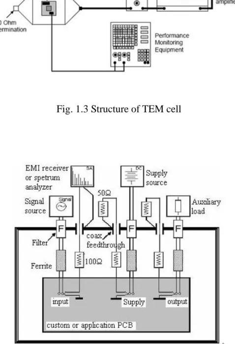
TEM cell actually is a deformed coaxial cable, in the medium of the coaxial cable, from a flat circuit board as the inner conductor, outer conductor is a square, one side coaxial cable connection to the test receiver, the other side connect the matches load, Fig. 1.3 is show the structure of TEM cell, on the outer conductor chamber top has a square opening for the installation and testing circuit boards, the circuit mounted on the side of a small side room, peripheral circuit outward, that makes measurement the radiation comes mainly from the measurement emission of circuit boards, test circuit boards produced high frequency current flow in the coaxial cable, those welding pin and package connections to act as a radiation transmitting antenna, when the TEM cell test frequency is lower than the first order high frequency modes, only the main mode TEM mode transmission, this TEM cell the voltage and the intensity of the emission source has a good quantitative relationship,
radiation emission.
1.3.2 Faraday Cage
Workbench faraday cage can test the power line and conducted interference voltage of the input and output signal line, will be equipped with a standard test board or an application board which is inserted into a small Faraday Cage, the power line and signal cables in and out of the faraday cage must through the filter, faraday cage test port connect test apparatus, other port connect matched 50Ω load, to assure shielding against electromagnetic environmental noise, therefore, the cable impedance is set to average 150Ω, measuring the voltage across the resistor to get the DUT RF radiation energy, test diagram shown in Fig. 1.4.
1.3.3 Magnetic Probe Method
Magnetic field probe measurement method is to use the magnetic field probe for measurement, because use the magnetic field probe for measurement, when measurement equipment is not necessary touch on the DUT, using this measurement method in the IC or power line of the noise current, the circuit board electromagnetic interference problems, often due to the IC circuit boards produced the noise current through the power line or the IC pin, the current flow to the IC and circuit board traces, and then
around the equipment or the circuit itself grounded back to the circuit board ground, the finally back to the IC's ground pin, this path form a closed loop, and this noise current flows through the circuit to larger, the electromagnetic interference are more serious, test diagram shown in Fig. 1.5.
1.3.4 Surface Scan Method
The surface scan method is a technique of measuring the radiated emissions from ICs by evaluating the near-field electromagnetic component over the surface of the package or the die in the frequency range from 10 kHz to 3GHz. In order to perform such an evaluation, the IC is scanned by a near-field electric or magnetic probe fabricated by using either a semi-rigid coaxial cable or PCB traces, the DUT has to be mounted on a dedicated test board and then placed in a test fixture to provide stability while the near-field probe is mechanically scanned by means of a mechanical probe positioning system. In particular, the probe is scanned over the DUT surface according to a programmed pattern while an automatic acquisition system makes possible the control of the scan parameters, the recovering and the processing of the collected data with the aim of representing the measured field strength by a colored two dimensional graphic at a given frequency, this method is capable of providing a detailed pattern of the emission sources within the DUT with a spatial resolution that depends from both the precision of the mechanical positioning system and the employed near-field antennas, test diagram shown in Fig. 1.6.
Although the measurements in many ways, but each method has drawbacks restricted, such as the standard TEM cell measurements, the size about the quarter wavelength, the space and frequency are limited, then Faraday Cage must have longer setup time and operation equipment is not easy to observe the waveform, so this research by the surface scan method to improve these problems, to achieve better results and the measurement accuracy.
1.4 Outline of thesis
This thesis consists of five chapters. This chapter provides an introduction and background on this research. Chapter 2 will introduce some theory of the antenna, such as the half wavelength dipole antenna、inverted F antenna, and Meander-line antenna will be used for the study. Chapter 3 presents a PIFA antenna designed for GSM-900 and 1800 MHz for the bands of the mobile phone. In addition, the dual-band PIFA antenna on handset design is evaluated experimentally and numerically in free space in proximity with head models of holding the antenna. Chapter 4 use the GEMS simulation tool to analysis the current distribution on the print circuit board. To analyze the cable and printed circuit board near the antenna radiation caused by the EMI problem. Chapter 5 is build high resolution circuit image. Chapter 6 is the conclusion.
Fig. 1.1 Structure of EMI problems from IC
Fig. 1.3 Structure of TEM cell
Fig. 1.4 Structure of Faraday Cage
Fig. 1.5 Structure of magnetic probe method
Chapter 2
Basic Theory of Antenna
2.1 Introduction
The main function of the antenna is the energy conversion and directional radiation, the circuit in the electrical signal and the free space electromagnetic coupling of energy conversion devices. If the antenna transmit signal, the antenna will conduct electrical energy into magnetic energy, the electromagnetic energy radiation into the surrounding environment, if the antenna received signal, the antenna receiving radiation energy into electrical energy supplied at the receiver.
2.2 Basic of monopole antenna
The monopole antenna is an ideal half-wave dipole antenna, by changing the image theory, first consider an infinite metal surface, if the dipole antenna feed point into the middle, and front into the metal surface on the front into a monopole antenna, the dipole antenna and monopole antenna structure are shown in Fig. 2.1, the monopole antenna is using a grounded metal surface to produce mirrored current, the physical length of the antenna impedance as long is as the dipole antenna input impedance of half, the impedance of the monopole antenna is from the half-wavelength dipole antenna theory to
know. 𝑍𝑖𝑛 = 𝑉𝑖𝑛,𝑚 𝐼𝑖𝑛,𝑚 = 1 2𝑉𝑖𝑛,𝑑 𝐼𝑖𝑛,𝑑 = 1 2𝑍𝑖𝑛,𝑑 (2.1)
If the monopole antenna is built on a metal surface, the EM waves radiation is only consider the half-plane metal surface, equivalent is only consider the dipole antenna in the upper half of the radiation waveform, so the radiation impedance is equivalent to half the dipole antenna.
𝑅𝑟,𝑚 = 𝑃𝑟𝑎𝑑,𝑚 1 2|𝐼𝑖𝑛,𝑚|2 = 1 2𝑃𝑟𝑎𝑑,𝑑 1 2|𝐼𝑖𝑛,𝑑|2 = 12𝑅𝑟𝑎𝑑,𝑑 (2.2)
The average per unit area radiated power:
𝑈𝑎𝑣𝑒 =𝑃𝑟𝑎𝑑,𝑑
4π (2.3)
The monopole antenna and dipole antenna directivity relation is:
𝐷𝑑 = 𝑈𝑚 𝑈𝑎𝑣𝑒 = 𝑈𝑚 𝑃𝑟𝑎𝑑,𝑑 4π (2.4) D𝑚 = 𝑈𝑚 𝑃𝑟𝑎𝑑,𝑚 4π = 𝑈𝑚 1 2 𝑃𝑟𝑎𝑑,𝑑 4π = 2𝐷𝑑 (2.5)
Inverted F antenna is change from inverted L antenna, the inverted L antenna is a monopole antenna and a grounded plane composition, the tradition design experience of inverted L antenna, the horizontal length about λ / 4, the perpendicular to the length of the horizontal section are small, the impedance characteristics similar a short monopole antenna, but inverted L antenna often difficult to achieve good impedance matching, the inverted F antenna is reference the inverted L antenna to improve the defect, the inverted F antenna using one end of the grounding mechanism to achieve good impedance matching effect, the basic structure shown in Fig. 2.2, with the monopole antenna have similar characteristics, include a small area, easy to manufacture etc...the antenna characteristics of relatively less susceptible to other external factors, such as hand or close to the body, the antenna characteristics will change with frequency, efficiency and antenna gain will substantially drop, the inverted F antenna have short-circuit in structure, so the module can reduce the metal interference, to achieve effective resist noise function, so most of inverted F antenna used in mobile communication systems.
2.4 Basic of meander-line antenna
In order to achieve the essential physical length of the antenna, and reduce the size placing in the mobile device, general used methods are meander-line and helix, the meander-line antenna is monopole antenna bent
other, the electromagnetic signal will interfere with each other, it causing the antenna to receive electromagnetic energy can’t be effective, so that the antenna efficiency will be reduce. Therefore, meander-line antenna are choose the antenna efficiency or antenna size, according to different applications and make readjust, meander-line dipole antenna structure shown in Fig. 2.3, structure parameters is shown in Table 2.1.
2.5 Summary
Antennas in wireless communications are extensively applications, the demand and requirement are different, how to develop these characteristics for suitable antenna is very difficult, not only to consider the antenna characteristics, when the antenna combined with the system to solve the different interference and problem are very important.
Fig. 2.1 Structure of the dipole and monopole antenna.
S L
H
L + H ≅λ
4
Fig. 2.3 Structure of meander-line dipole antenna.
Chapter 3
Design 900/1800 MHz PIFA Antenna on a mobile phone with a Proximate Head
3.1 Introduction
This section will design a dual-band PIFA antenna for mobile communication system (GSM900, GSM1800) , the proposed antenna is used meander-line structure, reduce the antenna size, and by bending the antenna approaches the resonant frequency 50Ω impedance, the structure is no need additional matching circuit to achieve the purposed antenna.
3.2 PIFA antenna design
This chapter uses the meander-line design a dual band PIFA antenna, Fig. 3.1 shows the PIFA antenna structure, antenna substrates is using FR4, the relative permittivity εr is 4.4, the thickness is 0.8 mm, and loss tangent is 0.027, because the PIFA antenna structure with a short line, the antenna's resonant length is from 1/2λ reduced to 1/4λ, meander-line structure can reduce the antenna size, the total size of the antenna is 60 mm × 70 mm, The right side meander-line inspire 900 MHz, the total length is 43 mm, The left side meander-line inspire 1800 MHz, total length is 17 mm, the transmission line length is 56 mm, and then use the distance between short
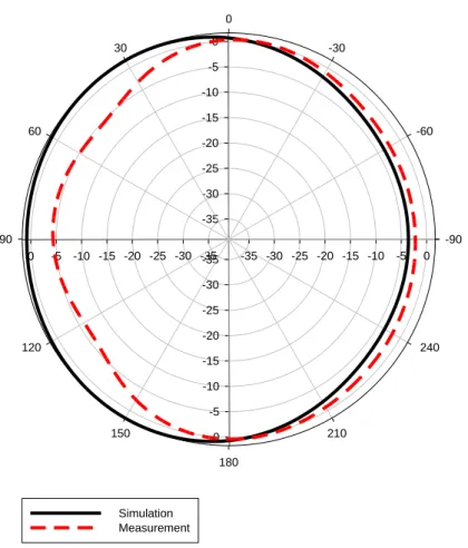
line and ground to adjust the capacitance and inductance to achieve good impedance matching, Figs. 3.2,3.3 show the reflection coefficient and Smith Chart of the antenna. Figs. 3.4,3.5 show the antenna efficiency, 900 MHz is 40%, 1800 MHz is 60%, Figs.3.6,3.7 show the antenna gain, 900 MHz is -0.5dBi and 1800 MHz is 3.5dBi. Figs. 3.8,3.9 show the 2D E and H-plane radiation pattern at 900 MHz, it can find the H-plane radiation pattern is almost omni-direction, Figs. 3.10,3.11 show the the 2D E and H-plane radiation pattern at 1800 MHz, it can find the radiation pattern at H-Plane is almost omni-direction, simultaneously, use this PIFA antenna replace PCB, simulation and analysis the electric field and surface current, Figs.3.12,3.13 show electric field and surface current at 900 MHz, and the Figs.3.14,3.15 show electric field and surface current at 1800 MHz, it can find the current distribution in the different planes.
3.3 Simulation of PIFA antenna with head model
As wireless communication technology fast development, the mobile communications have become a daily life indispensable, in the communications market, the competition will be intense, the enterprise are devoted how to improve the communication quality, this chapter use numerical simulation methods to explore the wireless mobile communication antennas, the antenna and human body electromagnetic coupling will effect mobile communications, this simulation use a simulation model as a human model, depend to different frequencies, relative permittivity and distance,
assessment the body affected of the antenna performance, It's a very important parameters and factor, Impact of human body for the antenna characteristics simulation results for the wireless mobile communication, antenna, RF circuit design and communication system planning have considerable help, Fig. 3.16 shows simulation structure, simulate the antennas and human body model at distance the 5,15 and 50 mm.
3.4 Simulation and measurement results
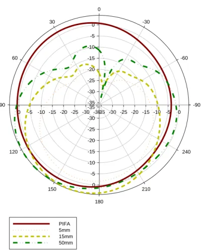
Fig. 3.17 shows the simulation reflection coefficient at different distances, Fig. 3.18 shows simulation antenna efficiency at 900 MHz with different distances are 5%, 20% and 58%, Fig. 3.19 shows the simulation antenna efficiency at 1800 MHz with different distances are 17%,45% and 78%, Fig. 3.20 shows the simulation antenna gain at 900 MHz with different distances are -8.5dBi,-1.5dBi and 4.5dBi, Fig. 3.21 shows the simulation antenna gain at 1800 MHz with different distances are -0.3dBi,4.5dBi and 5dBi, Fig. 3.22 shows 900 MHz simulation E-plane pattern with different distances, when the antenna closer to the human body model, the electromagnetic waves are absorbed more serious. Fig. 3.23 shows 900 MHz simulation H-plane pattern with different distances, when the distance of the antenna and human model is 5 mm, 15 mm and 50 mm, antenna radiation power affected the situation is more serious, Fig. 3.24 shows 1800 MHz simulation E-plane pattern at different distances, Fig. 3.25 shows 1800 MHz simulation H-plane pattern at different distances, table 3-1 shows simulation Antenna efficiency and gain with different distances.
The measurement structure as shown in Fig. 3.26, In this thesis, antenna measured by SATIMO measurement system, Fig. 3.27 shows the measurement reflection coefficient at different distances, Fig. 3.28 shows measurement antenna efficiency at 900 MHz with different distances are 4%, 22% and 34%, Fig. 3.29 shows the measurement antenna efficiency at 1800 MHz with different distances are 22%, 50% and 53%, it can find the antenna closed to the head model, antenna radiation energy is absorbed, Fig. 3.30 shows the measurement antenna gain at 900 MHz with different distances are -9.5dBi, -2.5dBi and 0.2dBi, Fig. 3.31 shows the measurement antenna gain at 1800 MHz with different distances are 2dBi, 4.3dBi and 5dBi, it can find the antenna gain easy to impact of the low frequency, when the distance are 50mm, the head model similar a reflection plane, antenna gain will raise, Fig. 3.32 shows 900 MHz measurement E-plane pattern with different distances, Fig. 3.33 shows 900 MHz measurement H-plane pattern with different distances, it can find the antenna closed to the head model, antenna radiation energy is absorbed, Fig. 3.34 shows 1800 MHz measurement E-plane pattern at different distances, Fig. 3.35 shows 1800 MHz measurement H-plane pattern at different distances.
3.5 Summary
importance, but the wireless communication standard for wireless transmission distance is very stringent, so it can’t heighten the wireless transmitter power, if want to extend the transmission range, height antenna reception sensitivity and antenna gain are methods, but the human body will be reflection and absorption in the antenna radiation and cause attenuation of the radiation performance, so the related communication system design must consider antenna placed of near human body, the communication system need to improve the quality of communication, and to limit the specific absorption rate (SAR) on the human body, through the numerical simulation results, hoping to reduce the phone's SAR value with the achieve better communication quality to make a balance.
Fig.3.1 PIFA antenna structure. Frequency(GHz) 0.5 1.0 1.5 2.0 2.5 3.0 |S 11|(dB) -25 -20 -15 -10 -5 0 Simulation Measurement
Fig.3.3 Dual-band PIFA antenna Smith Chart.
Fig.3.4 PIFA antenna efficiency at 900MHz.
900MHz 1800MHz Frequency(GHz) 0.80 0.85 0.90 0.95 1.00 Ef fi cenc y (linear ) 0.0 0.2 0.4 0.6 0.8 1.0 Simulation Measurement
Fig.3.5 PIFA antenna efficiency at 1800MHz.
Fig.3.6 PIFA antenna gain at 900MHz.
Frequency(GHz) 1.70 1.75 1.80 1.85 1.90 Ef fi cenc y (linear ) 0.0 0.2 0.4 0.6 0.8 1.0 Simulation Measurement Frequency(GHz) 0.80 0.85 0.90 0.95 1.00 Gain(dB i) -12 -10 -8 -6 -4 -2 0 2 Simulation Measurement
Fig.3.7 PIFA antenna gain at 1800MHz.
Fig.3.8 PIFA antenna in E-Plane pattern at 900MHz.
-35 -30 -25 -20 -15 -10 -5 0 -35 -30 -25 -20 -15 -10 -5 0 -35 -30 -25 -20 -15 -10 -5 0 -35 -30 -25 -20 -15 -10 -5 0 -90 -60 -30 0 30 60 90 120 150 180 210 240 Simulation Measurement Frequency(GHz) 1.70 1.75 1.80 1.85 1.90 Gain(dB i) -1 0 1 2 3 4 5 Simulation Measurement
Fig.3.9 PIFA antenna in H-Plane pattern at 900MHz. -35 -30 -25 -20 -15 -10 -5 0 -35 -30 -25 -20 -15 -10 -5 0 -35 -30 -25 -20 -15 -10 -5 0 -35 -30 -25 -20 -15 -10 -5 0 -90 -60 -30 0 30 60 90 120 150 180 210 240 Simulation Measurement -35 -30 -25 -20 -15 -10 -5 0 -35 -30 -25 -20 -15 -10 -5 0 -35 -30 -25 -20 -15 -10 -5 0 -35 -30 -25 -20 -15 -10 -5 0 -90 -60 -30 0 30 60 90 120 150 180 210 240 Simulation Measurement
Fig.3.11 PIFA antenna in H-Plane pattern at 1800MHz.
Fig. 3.12 Simulation electric field at 900MHz.
-35 -30 -25 -20 -15 -10 -5 0 -35 -30 -25 -20 -15 -10 -5 0 -35 -30 -25 -20 -15 -10 -5 0 -35 -30 -25 -20 -15 -10 -5 0 -90 -60 -30 0 30 60 90 120 150 180 210 240 Simulation Measurement
Fig. 3.13 Simulation surface current at 900MHz.
Fig. 3.15 Simulation surface current at 1800MHz.
Fig.3.16 Simulation structure.
Fig.3.17 Simulation reflection coefficient at different distances.
Fig.3.18 Simulation antenna efficiency at 900MHz with different distances.
Frequency(GHz) 0.5 1.0 1.5 2.0 2.5 3.0 |S 11|( dB) -30 -25 -20 -15 -10 -5 0 PIFA 5mm 15mm 50mm Frequency(GHz) 0.80 0.85 0.90 0.95 1.00 Ef fi c ienc y 0.0 0.2 0.4 0.6 0.8 1.0 PIFA 5mm 15mm 50mm
Fig.3.19 Simulation antenna efficiency at 1800MHz with different distances.
Fig.3.20 Simulation antenna gain at 900 MHz with different distances.
Frequency(GHz) 1.70 1.75 1.80 1.85 1.90 Ef fi c ienc y 0.0 0.2 0.4 0.6 0.8 1.0 PIFA 5mm 15mm 50mm Frequency(GHz) 0.80 0.85 0.90 0.95 1.00 Gain( dBi) -12 -10 -8 -6 -4 -2 0 2 4 6 PIFA 5mm 15mm 50mm
Fig.3.21 Simulation antenna gain at 1800MHz with different distances. -35 -30 -25 -20 -15 -10 -5 0 -35 -30 -25 -20 -15 -10 -5 0 -35 -30 -25 -20 -15 -10 -5 0 -35 -30 -25 -20 -15 -10 -5 0 -90 -60 -30 0 30 60 90 120 150 180 210 240 PIFA 5mm 15mm 50mm Frequency(GHz) 1.70 1.75 1.80 1.85 1.90 Gain( dBi) -2 -1 0 1 2 3 4 5 6 PIFA 5mm 15mm 50mm
-35 -30 -25 -20 -15 -10 -5 0 -35 -30 -25 -20 -15 -10 -5 0 -35 -30 -25 -20 -15 -10 -5 0 -35 -30 -25 -20 -15 -10 -5 0 -90 -60 -30 0 30 60 90 120 150 180 210 240 PIFA 5mm 15mm 50mm -35 -30 -25 -20 -15 -10 -5 0 -35 -30 -25 -20 -15 -10 -5 0 -35 -30 -25 -20 -15 -10 -5 0 -35 -30 -25 -20 -15 -10 -5 0 -90 -60 -30 0 30 60 90 120 150 180 210 240 PIFA 5mm 15mm 50mm
Fig.3.23 Simulation 900 MHz H-plane pattern at different distances.
-35 -30 -25 -20 -15 -10 -5 0 -35 -30 -25 -20 -15 -10 -5 0 -35 -30 -25 -20 -15 -10 -5 0 -35 -30 -25 -20 -15 -10 -5 0 -90 -60 -30 0 30 60 90 120 150 180 210 240 PIFA 5mm 15mm 50mm
Fig.3.25 Simulation 1800 MHz H-plane pattern at different distances.
Table 3.1 Simulation antenna efficiency and gain with different distances.
900MHz Efficiency 900MHz Gain 1800MHz Efficiency 1800MHz Gain PIFA 0.60 0.2 0.88 3.2 5mm 0.05 -8.5 0.17 -0.3 15mm 0.20 -1.5 0.45 4.5 50mm 0.58 4.5 0.78 5
Fig.3.26 Measurement structure. Frequency(GHz) 0.5 1.0 1.5 2.0 2.5 3.0 |S 11|( dB) -20 -15 -10 -5 0 PIFA 5mm 15mm 50mm
Fig.3.27 Measurement reflection coefficient with different distances.
Fig.3.28 Measurement antenna efficiency at 900 MHz with different distances.
Fig.3.29 Measurement antenna efficiency at 1800 MHz with different
Frequency(GHz) 0.80 0.85 0.90 0.95 1.00 Ef fi c ienc y (linear ) 0.0 0.2 0.4 0.6 0.8 1.0 PIFA 5mm 15mm 50mm Frequency(GHz) 1.70 1.75 1.80 1.85 1.90 Ef fi c ienc y (linear ) 0.0 0.2 0.4 0.6 0.8 1.0 PIFA 5mm 15mm 50mm
Fig.3.30 Measurement antenna gain at 900 MHz with different distances.
Fig.3.31 Measurement antenna gain at 1800 MHz with different distances.
Frequency(GHz) 0.80 0.85 0.90 0.95 1.00 Gain( dBi) -12 -10 -8 -6 -4 -2 0 2 PIFA 5mm 15mm 50mm Frequency(GHz) 1.70 1.75 1.80 1.85 1.90 Gain( dBi) 0 1 2 3 4 5 6 7 PIFA 5mm 15mm 50mm
Fig.3.32 Measurement 900 MHz E-plane pattern with different distances.
Fig.3.33 Measurement 900 MHz H-plane pattern with different distances.
-40 -35 -30 -25 -20 -15 -10 -5 -40 -35 -30 -25 -20 -15 -10 -5 -40 -35 -30 -25 -20 -15 -10 -5 -40 -35 -30 -25 -20 -15 -10 -5 -90 -60 -30 0 30 60 90 120 150 180 210 240 PIFA 5mm 15mm 50mm -40 -35 -30 -25 -20 -15 -10 -5 0 -40 -35 -30 -25 -20 -15 -10 -5 0 -40 -35 -30 -25 -20 -15 -10 -5 0 -40 -35 -30 -25 -20 -15 -10 -5 0 -180 -150 -120 -90 -60 -30 0 30 60 90 120 150 PIFA 5mm 15mm 50mm
Fig.3.34 Measurement 1800 MHz E-plane pattern with different distances.
Fig.3.35 Measurement 1800 MHz H-plane pattern with different distances. -40 -35 -30 -25 -20 -15 -10 -5 0 -40 -35 -30 -25 -20 -15 -10 -5 0 -40 -35 -30 -25 -20 -15 -10 -5 0 -40 -35 -30 -25 -20 -15 -10 -5 0 0 30 60 90 120 150 180 210 240 270 300 330 PIFA 5mm 15mm 50mm -40 -35 -30 -25 -20 -15 -10 -5 0 -40 -35 -30 -25 -20 -15 -10 -5 0 -40 -35 -30 -25 -20 -15 -10 -5 0 -40 -35 -30 -25 -20 -15 -10 -5 0 -180 -150 -120 -90 -60 -30 0 30 60 90 120 150 PIFA 5mm 15mm 50mm
Chapter 4
Simulation and Measurement of RE for PCB
4.1 Introduction
The electromagnetic interference can be divided into three elements, it includes the noise source, the receiving, and the transmission path, the three elements are electromagnetic interference, electromagnetic susceptibility, and transmission mode. In the printed circuit board, the electromagnetic interference noise model can be divided into conduction and radiation mode, the two kind’s interferences except on different transmission medium and frequency. In the past, the electromagnetic interference definition is mutual influence of the systems to system, but the circuit system is increasingly complex, a circuit system is often not only a circuit subsystem exists, the system gradually unable to ignore interaction between the subsystems, so the electromagnetic interference problem does not only exist in systems to system, it must consider to the subsystem problem, the problem can be get the best resolution.
4.2 Design and analysis of PIFA antenna for the electric field
distribution
ambient electronic components will interfere and affect the product performance, EMC with the current, electric and magnetic fields and electromagnetic radiation coupling phenomena are related, coupling occurs in two ways. Are electric field coupling and magnetic coupling, the antenna from the radiation source coupled to the circuit noise, it could be the magnetic field coupling or both, how to control them? It must understand the coupling mechanism, and how to impact product. An example of communication system is shown in Fig. 4.1, the electronic circuit structure is very complex, it include many coaxial cable and electronic components, it will to cause interference if it near the antenna, EMI radiation is not broadband, the system will excite the resonance, the external cable maybe excitation the resonance.
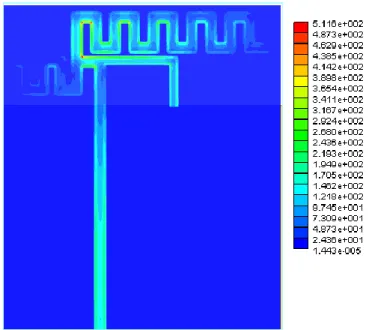
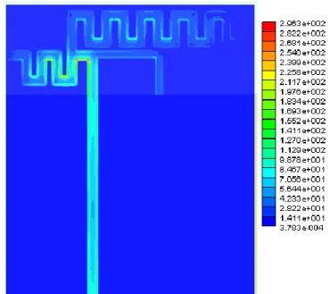
Fig. 4.2 shows in simulation the antenna radiation, the current distribution of the coaxial cable; it can be find the current distribution of the different polarization. Fig. 4.3 is the simulation the sensitive electronic components from antenna radiation to receive the interfere and sense current, it can find the current strength in the simulation area, to improve the electromagnetic interference and enhance product performance, this chapter use PIFA antenna of the previous chapter to simulate the antenna radiation with electric field in the distribution of different distances, simulated distance at 0.3 cm, 0.5 cm and 1 cm, the effects of different distances of the surrounding electric field and current distribution.
This part, use the GEMS to simulate the current density on the PCB, the GEMS is based on the FDTD, the simulation distance is 0.3 cm, the simulation area is shown in Fig. 4.4, it use a PIFA antenna to replace PCB, to simulated electric field at 900 MHz and 1800 MHz is shown in Fig. 4.5 and Fig. 4.6. Fig.4.7 is shown the hardware implementation of the antenna, using the probe to scan the surface and recording results, the aperture field for meander line PIFA with simulated and measured at 900 MHz and 1800 MHz are shown in Fig. 4.8 and Fig. 4.9. The results of simulation and measurement are similar.
4.4 Summary
The wireless communications are more popular in nowadays. Most of the size of cellular in communications is compact with smaller size. The RF components on the PCB of cellular will have mutual electromagnetic interference. If the components of receiver are interfered by near field RF components, the total isotropic sensitivity (TIS) of cellular will be degraded. The antenna is compact and near the PCB of cellular phone. The efficiency of antenna will also be degraded. Not only the total radiation power (TRP) but also the TIS will be reduced. The performance, such as throughput, bit error rate (BER) of cellular communication systems will be degraded due to the low TRP and TIS. The near field EMI of PCB is quite important for compact size communication systems, but how to measure the electromagnetic interference and locate the EMI sources on PCB is not an easy job, in next
Fig.4.1. Structure communication system.
Fig.4.3. Simulated electric current.
Fig.4.5. Simulated surface current density at 900 MHz.
Fig.4.7. Aperture field scan of antenna.
Chapter 5
Build High Resolution Circuit Image
5.1 Introduction
In this chapter, how to solve the EMI of PCB to improve the performance of communication systems? By special arrangement of RF components on PCB will enhance the TIS and TRP of communications. How to measure the electromagnetic interference and locate the EMI sources on PCB is not an easy job. This chapter proposes the aperture field technique to get the high resolution surface current density on the PCB. In order to verify the technique, simulation the PIFA antennas with surface current density and near aperture field on PCB are analyzed by GEMS. Except for the simulation, PIFA antennas are implemented and aperture field are collected by planar near field range. By using aperture field transformation to the surface of PCB, the surface current density on the PCB is obtained.
5.2 Diffraction field by NF aperture
Fig. 5.1 shows in the aperture antenna radiation diagram, while the S is the radiation source region, the position vector of source point , on the
aperture is:
x
ˆ
y
ˆ
(5.1)(5.2)
,A is the magnitude of field intensity,
, is the phase of the field intensity, Fˆ is the polarization unit vector of source point.The diffraction field intensity at fixed
R,,
is:
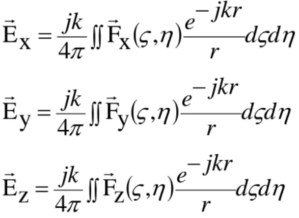
(5.3)
When the boundary conditions not any restrictions, if the location of the observation point placed in the far field range, because distance faraway, the radiation source to the observation point R and the origin point from the observation point r can be regarded as nearly parallel to line, 𝑛̂ ∙ 𝑟̂ = 𝑛̂ ∙ 𝑅̂ = cos θ , 𝑎𝑛𝑑 1𝑟 ≪ k = 2πλ, then
(5.4)
Whether radiation source or the distribution of the radiation field, even integration of the radiation field, use the Cartesian coordinates to expression is most appropriate, in the integral particular solution, there are three most common and convenient way of expression the plane, there are y-z plane, x-z plane, x-y plane, as shown in the Fig.5.2, if the three planes were used to analyze the distribution of the radiation field, the integral will be different. Nevertheless, even the different integral of the different plane, the calculated result will be the same, the actual distribution of the radiation field. At different plane respectively:
n
s
d
d
r
jkr
e
jk
cos
ˆ
ˆ
,
F
4
,
R,
E
n r jkn s d
d
r jk r jkr e F , 1 ˆ ˆ ˆ ˆ 4 1 , R, E
,
,
,
F
ˆ
F
A
e
j
(5.5)
(5.6)
(5.7)
Radiation from the source to the different observation points of the path integral :
(5.8)
Because it inability to know the actual surface current distribution, so using the equivalence principle, by the actual near field electric field transform to equivalent surface current.
Fig. 5.3 shows a simple example of the equivalence principle. In Fig. 5.3 (a) within the region of S is the actual source of the radiation field distribution, it include the flux current J and M, the M is imagine of the virtual field source, exterior is the free space, let S region exterior the radiation field and the medium retain, while the internal is presume no any radiation field, the internal become a free space, as shown in Fig. 5.3 (b). As the S region exterior still presence a radiation field, so the boundary of the S region, it will existence the surface current Js and the surface magnetic current Ms, as shown in equation 5.9. Js = n × H (5.9a) Ms = E × n (5.9b)
r
d
d
jkr
e
jk
F
x
,
4
x
E
r
d
d
jkr
e
jk
F
y
,
4
y
E
r
d
d
jkr
e
jk
F
z
,
4
z
E
] ) ( ) [(x0 2 y0 2 z2 r
The transformation formula structure as shown in Fig. 5.4, using measurement plane induct the magnetic field energy, equivalent to the surface current distribution on the PCB, as shown in equation 5.10.
J⃗=ẑ × (Hxx̂+Hyŷ+Hzẑ) (5.10)
From equation 5.10, it can equivalent to the surface current.
𝐽𝑥=−𝐻𝑦 (5.11a)
𝐽𝑦=𝐻𝑥 (5.11b)
5.3 Simulation and test results
In this part, it will use simulation tools to simulated the near field electric field and surface current distribution in the different distances are 0.3 cm, 0.5 cm 1 cm, as shown in Fig.5.5, the simulated surface current for PIFA at 900 MHz and 1800 MHz is shown in Fig.5.6 and Fig.5.7. It can find the distribution of the surface current at different frequency, the Fig.5.8 and Fig.5.9 are show the simulated magnetic field density with the distance at 0.3 cm in 900 MHz and 1800 MHz, the Fig.5.10 and Fig.5.11 are show the simulated magnetic field density with the distance at 0.5 cm in 900 MHz and 1800 MHz, Fig.5.12 and Fig.5.13 are show the simulated magnetic field density with the distance at 1cm in 900 MHz and 1800 MHz, sorting out the simulation data of the magnetic field density, it can use the results, by the
current density on the PCB.
The surface current density is transformed from the aperture field by the formula. Fig.5.14 as shown in transformation formula structure with different scope, the transformation scope are 3.5 mm*3.5 mm and 6.5 mm*6.5 mm, when the measurement plane and antenna surface to farther, the integration range must to raise, the Fig.5.15 and Fig.5.16 are show the transformed surface current with the distance at 0.3 cm in 900 MHz and 1800 MHz and the integration range is 3.5 mm*3.5 mm, the Fig.5.17 and Fig.5.18 are show the transformed surface current with the distance at 0.3 cm in 900 MHz and 1800 MHz and the integration range is 6.5 mm*6.5 mm, it can find integration range will affect intensity of the surface current, the Fig.5.19 and Fig.5.20 are show the transformed surface current with the distance at 0.5 cm in 900 MHz and 1800 MHz, Fig.5.21 and Fig.5.22 are show the transformed surface current with the distance at 1cm in 900 MHz and 1800 MHz, The results of transformed surface current from transformation and simulation are quite similar.
5.4 Summary
Most of radiation emission (RE) from PCB will cause the system fail to pass the EMI regulation and degradation the sensitivity in communication system. Since the size of cellular communication system is smaller and smaller, the sensitivity of system is degraded by near field EMI. This chapter proposes a technique to predict the high resolution surface current density on PCB by planar aperture field above the PCB and current density on the PCB.
The aperture field of PCB antenna with dual bands are measured by planar near field scanner. The measured data is transformed to the surface of PCB to get the surface current density on the PCB. The results of PCB current density from both measurement and simulation are quite similar.
Fig.5.1 the diffraction field by near field aperture.
Fig.5.2 (a) Plane position and rectangular aperture antenna radiation analysis: x-z plane.
dz
dx
Fig.5.2 (b) Plane position and rectangular aperture antenna radiation analysis: y-z plane.
Fig.5.2 (c) Plane position and rectangular aperture antenna radiation
analysis: x -y plane.
dy
dx
dy
Fig.5.3 Equivalence principle.
Fig.5.5 PIFA antenna structure.
Fig. 5.7 Surface current at 1800 MHz.
Fig. 5.9 Magnetic field at distance 0.3cm in 1800MHz.
Fig. 5.11 Magnetic field at distance 0.5 cm in 1800 MHz.
Fig. 5.13 Magnetic field at distance 1 cm in 1800 MHz.
Fig. 5.15 Transformed surface current at distance 3mm in 900 MHz.
Fig. 5.17 Transformed surface current at distance 3mm in 900 MHz.
Fig. 5.19 Transformed surface current at distance 5mm in 900 MHz.
Fig. 5.21 Transformed surface current at distance 1cm in 900 MHz.
Chapter 6
Conclusion
The EMI / EMC problem is prompted by the current on the conductor change to generated electromagnetic radiation; similarly, the external electromagnetic field energy can also be changes the circuit current. Most of high-speed and fast rise time signal will produce the EMI / EMC problems, these problems will be connected to the equipment the cable, the typical solution is shield and filter on the input and output signals on power line. This thesis proposes the aperture field technique to get the high resolution surface current density on the PCB, by using aperture field transformation to the surface of PCB, the surface current density on the PCB is obtained. Almost all of EMI interference is produce current in the product of the somewhere, if these currents can be properly controlled, it only contains work required for the harmonic, reduce the high frequency harmonic unnecessary interference, the EMI / EMC problems will be solved. If during the design phase, can consideration the EMC problem, it will be save time and cost.
References
[1] GEMS, 3-D High Performance parallel EM simulation Software, www.2comu.com.
[2] Chuan-Fu Wu “EMC control and prevention” 2008
[3] Yonh-Zong Chen, Ren-Yu Gu, “The Study of Measurement Theorem and Prevention over Electromagnetic Interference Environment and RF Noise” Da-Yeh University, 2005
[4] Wen-Shi Lee, Yi-Shen Chen,“900/1800MHz dual-band ceramic chip antenna bandwidth improvement and equivalent circuit simulation and analysis” National Cheng Kung University, 2005
[5] Chi-Fang Huang, Yao-Ting Huang, “Realization of Compact Quadrifilar Helix Antennas” Tatung University, 2008
[6] Szu-shun Pai, “Strategy of EMI Reduction for Power Ground Planes in Multi-Layer PCB Design”, Tatung University, 2006
[7] Wein-Long Lin, “Design and Analysis of Standard Noise Source for Electromagnetic Interference”, Da-Yeh University, 2004
[8] Cheng-Wei Chen, “Antenna Design of Mobile Communication and Analysis of SAR Simulation” pp.108-131. January. 2011.
[9] Wei-Lu Hung, “Design and Study of Small PIFA Structures” pp.18-32. June. 2007.
[11] Chun-Yi Chen, “Analysis and Build the Planar Near-Field Measurement System” pp.20-37. June, 2003.
[12] Fang-I Hsu, “Planar Near-Field to Far-Field Transformation and PIFA Antenna Suitable for Wireless LAN” pp.9-23. June, 2002.
[13] Liang-Chen Kuo, “Numerical Study of EM Interaction of Handset
Antennas with Human Head Models and Planar WLAN Antenna Design by Using FDTD Method” pp.68-80. January, 2007.
[14] Jong-Pil Lee and Seong-Ook Park, “The Meander Line Antenna for Bluetooth” pp.1-3. January, 2002.
[15] Shih-Yi Chan, “The Application of Meander-Line Antenna to Mobile Communication” pp.35-61. June, 2005.
[16] Ken-Huang Lin, “Study and Implementation of the Log-Periodic Dipole Array Antenna for Electromagnetic Compatibility” pp.22-32. June, 2001. [17] Yen-Chi Shen, “Printed Triple-Band Antenna Utilizing Modified
Open-Loop and Switched Beam Antenna for Wireless Communication Applications” pp.20-29. July, 2006.
[18] Kun-Cheng Lai, “Design and Measurement of Ultra Wide Band Antenna” pp.21-37, July, 2008.
[19] Wen-Shan Chen, “Studies of Dual-Band and Broadband Printed Slot Antennas” pp.57-69, January, 2001.
[20] Yu Ting, Wu, “Study of Correlating TEM Cell and OATS Measurements for the Radiated Emission of IC” pp.23-39, July, 2007.
Integrity and EMI Performance in Multi-Layered High-Speed Digital PCB:FDTD Modeling and Measurement” pp.10-24, June, 2002
[22] Guo-Siang Hsiao,”The Application of Spread Spectrum Techniques in IC EMC Design” pp.50-69, July, 2008
[23] Chien-Hsun Chen,”TheEffect of Electromagnetic Wave and Human Head” pp.1-6, July, 2010