105 Interfacial Reactions between Liquid In and Ni Substrate
105
Regular Issue Paper Journal of Electronic Materials, Vol. 28, No. 2, 1999
INTRODUCTION
Soldering is a low-temperature joining process com-monly used for electronic packaging.1 During
solder-ing, the solder alloy melts and reacts with the sub-strate to form intermetallic compounds at the joining interface. The formation of intermetallic phases at the solder joint could cause mechanical failure during thermal or power cycling.2 Therefore, a knowledge of
intermetallic phases produced by soldering in elec-tronic packaging is essential. Among many solder alloys, Pb-Sn solders have been most commonly used.3
However, since Pb will induce environment pollution, the development of Pb-free solders should thus be of vital importance for the electronic industry in the future. Several Pb-free solders4,5 have been developed
for electronic packaging. Jin et al.6 developed a
Bi-43%Sn solder containing Fe dispersoid particles, which had better microstructure stability and superior creep resistance compared to the Pb-Sn eutectic solder. The growth kinetics of Ni-Sn intermetallic phases at the liquid Sn and solid Ni interface has been investigated by Kang et al.7 In their work, both Ni
3Sn4 and Ni3Sn2
were observed and parabolic kinetics was obeyed for the growth of intermetallic compounds.
The In-alloy solders possess a longer fatigue life
than conventional Pb-Sn solders for flip-chip inter-connections in thermal shock tests between room temperature and liquid nitrogen.8 Some studies have
been performed on the interfacial reactions between In and Cu. Kao9 found that Cu
11In9, Cu7In3, and Cu2In
formed in the solid Cu/liquid In interface. Manna et al.10 studied the interdiffusion between In and bulk
Cu and Cu-In alloy isothermally annealed at 373, 398, and 423K for varying lengths of time. They found the growth rates of intermetallic layers to follow para-bolic kinetics. The activation energy for Cu (In) inter-diffusion was 26.07 kJ/mol and for Cu-In (In) was 26.42 kJ/mol. With the exception of these efforts, no other information is yet available on the interfacial reaction between In and Ni.
In the present work, the morphologies and growth kinetics of intermetallic compounds during the reac-tion of liquid In with solid Ni were analyzed in the temperature range from 225 to 500°C. For the identi-fication of intermetallic compounds, both electron microprobe (EPMA) and x-ray diffraction (XRD) were employed.
EXPERIMENTAL
Nickel substrates (15 mm × 15 mm) were cut from a 0.8 mm thick high-purity Ni plate (Ni-99.5%). Their surfaces were prepared by grinding with 1500 grit SiC paper and polishing with 0.3 µm Al2O3 powder.
Interfacial Reactions between Liquid Indium
and Nickel Substrate
Y.H. TSENG,1 M.S. YEH,1,2 and T.H. CHUANG1
1.—Institute of Materials Science and Engineering, National Taiwan University, Taipei, Taiwan, R.O.C. 2.—Present Address: Department of Mechanical Engineering, Chung-Hua University, Hsin-Chu, Taiwan, R.O.C.
The morphologies and growth kinetics of intermetallic compounds for the interfacial reaction between liquid In and solid Ni substrate in the temperature range from 225 to 500°C are examined in this study. Experimental results showed that the thickness of intermetallic compounds formed during the Ni(s)/ In(l) interfacial reaction increased with the reaction temperature and the square root of reaction time. The x-ray diffraction pattern revealed the formation of intermetallic compounds Ni10In27 (T<300°C) and Ni2In3 (T>300°C). Moreover, the activation energies for the interdiffusion of Ni and In atoms in the Ni10In27 and Ni2In3 are 94.74 and 33.51 kJ/mol, respectively. Using the Ta thin film as a diffusion mark, the formation mechanism of intermetallic compounds during interfacial reaction was clarified.
Key words: Activation energy, indium, intermetallic compound, nickel
106 Tseng, Yeh, and Chuang
Indium plates (In-99.99%) with dimensions of 3 × 3 × 3 mm3 were laid on the Ni substrates. The SMQ
TACFLUX 005 flux was used in this test. Table I lists the characteristics of this flux.
Interfacial reactions were carried out at tempera-tures ranging from 225 and 500°C in an infrared furnace for various periods of time in a vacuum of 10–3
Torr. After the reactions, In was selectively etched from the Ni/In specimens using an aqueous solution of 7g NH4F + 10 ml H2O2. The intermetallic compounds were analyzed using XRD. In order to examine the growth kinetics of intermetallic compounds during interfacial reactions, the cross sections of all speci-mens were observed with a scanning electron micro-scope (SEM) and average thicknesses of the
interme-tallic layer were given for the analyses at five points. The In contents in intermetallic compounds were further examined by EPMA. The measurements are known to be within ±0.05 at.%. Combining the results of XRD and EPMA analyses, the intermetallic com-pounds that form through the interfacial reactions between liquid In and Ni substrate were identified. For further clarification of the formation mechanism of intermetallic compounds in the interfacial reac-tion, the original Ni(s)/In(l) interfaces were marked by sputtering-deposition of a Ta thin film on the partial region of Ni substrates. From the phase diagram, it can be seen that Ta will not react with Ni and In, the deposition of Ta thin film acted as a diffusion barrier at Ni(s)/In(l) interface. The original Ni(s)/ln(l) interface can thus be identified.
RESULTS AND DISCUSSION
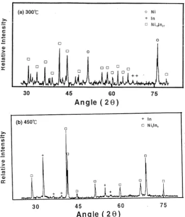
When the specimens were heated above the melting temperature of In (157°C), the molten In reacted with Ni substrate and immediately formed intermetallic compounds (NixIny) at the Ni(s)/In(l) interface. Accord-ing to the Ni-In phase diagram, several intermetallic phases such as Ni3In, Ni2In, Ni13In9, NiIn, Ni2In3, and Ni10In27 could form. However, the x-ray diffraction patterns only revealed the phases Ni, In, and Ni10In27 for the samples reacting below 300°C (Fig. 1a). When the reaction temperatures increased above 300°C, Ni, In, and Ni2In3 were detected (Fig. 1b). The chemical compositions of interfacial reaction products were also analyzed by using EPMA, the results are shown in Table II. In Table II, average data were given for the analyses at five points, revealing that the primary intermetallic compound formed below 300°C was Ni10In27, and above 300°C changed to Ni2In3.
The typical morphologies of Ni(s)/ln(l) interfacial microstructure in dependence of reaction tempera-tures and times are shown in Fig. 2. Small nuclei of intermetallic compounds are found randomly along the Ni/In interface at 250°C for 15 min, which re-vealed the early step of interfacial reaction (Fig. 2a). A continuous intermetallic layer grew slowly with the increase of reaction time (Fig. 2b). At 450°C, the continuous intermetallic layer formed even after a
Table I. The Characteristics of SMQ TACFLUX 005 Flux
Flux Type Flash Point Solid Content Viscosity (25°C ) Max. use Temp. Residue Removal
RMA 66°C 14% 68,000±10% cps 300°C Water
Fig. 1. Typical x-ray diffraction patterns of the Ni(s)/In(l) interfacial
reaction products formed below and above 300°C: (a) 300°C, and (b)
450°C.
Fig. 2. Typical morphologies of the Ni(s)/In(l) interfacial reaction products formed under various temperatures at various times: (a) 250°C, 15 min,
107 Interfacial Reactions between Liquid In and Ni Substrate
short reaction time of 15 min (Fig. 2c). Reaction at such an elevated temperature for a longer time caused the appearance of a very thick and uniform interme-tallic layer (Fig. 2d). It was also found that during the interfacial reactions, some products showed poor ad-hesion with the Ni substrate and separated from the interface to form many intermetallic islands in the In matrix. The remaining intermetallic products grew as a continuous layer along the Ni(s)/In(l) interface. EPMA analyses confirmed that both the intermetallic islands and the continuous intermetallic layer pos-sessed the same In content.
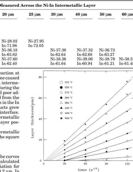
The average thicknesses (∆X) of the intermetallic layers were measured and plotted against the square root of the reaction time (t) in Fig. 3
∆X=K t
where K is the growth rate constant. From the curves of Fig. 3, the growth rate constants were calculated and listed in Table III. The standard deviation for intermetallic layers was between 0.1 and 0.2 µm. In Fig. 3, it can be seen that the growth of intermetallic compounds followed a parabolic law, implying that the growth of the intermetallic layer was diffusion controlled; i.e., the Ni and In atoms interdiffused through the intermetallic compound layer to result in the growth of intermetallic compounds. In this case, the Arrhenius equation can be used to express the growth rate constant for the intermetallic layer:
K A Q
RT = exp−
where A is a constant, Q is the activation energy, R is the gas constant, and T is the absolute temperature. An Arrhenius diagram of ln K vs 1/T is given in Fig. 4. The diagram consists of two straight lines inter-secting at approximately 300°C, which indicates that two kinds of intermetallic compounds grew in differ-ent temperature ranges during the Ni(s)/In(l) interfa-cial reaction. The activation energies for the straight line above and below 300°C, as determined from Fig. 4, were 94.74 and 33.51 kJ/mol, respectively. Accord-ing to the XRD and EPMA analyses presented above, the interfacial reaction in the temperature range
from 300 to 500°C resulted in an Ni2In3 intermetallic compound. Below 300°C, the Ni10In27 compound was found. This implied that the activation energies for the interdiffusion of Ni and In atoms in the Ni2In3 and Ni10In27 intermetallic compounds were 94.74 and 33.51 kJ/mol, respectively.
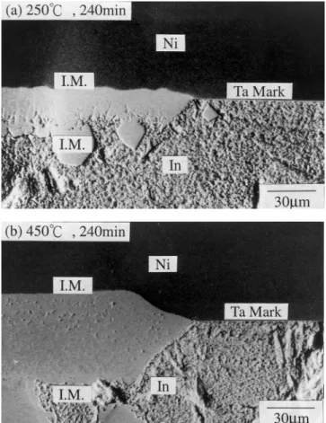
Through the employment of Ta thin film on Ni substrate as a diffusion barrier for the Ni(s)/In(l) inter-facial reaction, it was found that the reaction fronts of intermetallic compounds migrated toward Ni sub-strate and molten In (Fig. 5). EPMA analyses showed that the intermetallic compounds on both sides of the Ta diffusion mark possessed the same In contents. It was also shown that the ratios of migration distance toward Ni substrate to that toward molten In were about 2.25 and 2.10 for the interfacial reactions below and above 300°C, respectively. The ratio of migration distance toward Ni substrate to that toward In solder should correspond to the ratio of diffusivity (D) of In and Ni in the respective intermetallic compounds.
Table II. Chemical Compositions Obtained Across the Intermetallic Layer Formed during Ni(s)/In(l) Interfacial Reaction (at.%)
Positions Measured Across the Ni-In Intermetallic Layer
5µm 10 µm 15 µm 20 µm 25 µm 30 µm 40 µm 50 µm 60 µm
250°C Ni-29.62 Ni-29.25 In-70.38 In-70.75
275°C Ni-27.76 Ni-26.16 Ni-26.74 In-72.24 In-73.84 In-73.26
300°C Ni-28.96 Ni-28.01 Ni-28.47 Ni-28.02 Ni-27.95 In-71.04 In-71.99 In-71.53 In-71.98 In-72.05
450°C Ni-36.75 Ni-36.18 Ni-37.36 Ni-37.32 Ni-36.73
In-63.82 In-63.82 In-62.64 In-62.68 In-63.27
500°C Ni-38.06 Ni-37.60 Ni-38.36 Ni-39.06 Ni-38.79 Ni-38.52
In-61.94 In-62.40 In-61.64 In-60.94 In-61.21 In-61.48
Fig. 3. Thickness of intermetallic compound layers as a function of the square root of reaction time under the reaction temperature range from 225 to 500°C.
108 Tseng, Yeh, and Chuang i.e., D D and D D Ni Ni In In Ni In Ni Ni In In Ni In / / / / . . . 10 27 10 27 2 3 2 3 5 07 4 43 = = CONCLUSIONS
Two kinds of intermetallic compounds, Ni10In77 and Ni2In3 for temperatures below and above 300°C, re-spectively, form when polycrystalline Ni substrates react with liquid In. The thickness of the intermetallic compounds formed during Ni(s)/In(l) interfacial reac-tion increased with the reacreac-tion temperature and the square root of reaction time, which implies that the reaction is diffusion controlled. i.e., during the inter-facial reaction of Ni substrate and molten In, Ni, and In atoms interdiffused through intermetallic pounds to cause the growth of intermetallic
com-Table III. Growth Rate Constants of Intermetallic Layers Formed during the
Ni(s)/ln(l) Interfacial Reaction
Growth Rate Constant
Temperature(°C) (cm2s–1) 225 3.32 × 10⁻¹¹ 250 1.30 × 10⁻¹⁰ 275 1.59 × 10⁻¹⁰ 300 6.56 × 10⁻¹⁰ 350 1.06 × 10⁻⁹ 400 1.76 × 10⁻⁹ 450 2.80 × 10⁻⁹ 500 3.92 × 10⁻⁹
Fig. 5. Migration of reaction of intermetallic compounds at Ni(s)/In(l)
interface formed below and above 300°C: (a) 250°C, 240 min, and (b)
450°C, 240 min.
Fig. 4. Arrhenius plots of the growth rate constant (ln K) vs reaction
temperature (1/T) during the Ni(s)/In(l) interfacial reaction.
pounds. The activation energies for the interdiffusion of Ni and In atoms in the Ni10In27 (T<300°C) and Ni2In3 (T>300°C) are 94.74 and 33.51 kJ/mol, respec-tively. Using the diffusion mark of Ta thin film, the ratios of the diffusivity for In to Ni in Ni10In27 and in Ni2In3 were approximately 5.07 and 4.43, respec-tively.
REFERENCES
1. R.R. Tummala and E.J. Rymaszewski, Microelectronics
Pack-aging Handbook, (New York: Van Nostrand Reinhold, 1989).
2. G.D. O’clock Jr., M.S. Peters, J.R. Patter, G.A. Kleese and R.V. Martini, IEEE Trans. Comp. Hybirds, Man. Tech. CHMT-10, 82 (1987).
3. J.O.G. Parent, D.D.L. Chung and I.M. Bernstein, J. Mater.
Sci. 23, 2564 (1988).
4. S.K. Kang and A.K. Sarkhel, J. Electron. Mater. 23, 701 (1994).
5. M. McCormack, S. Jin and G.W. Kammlott, IEEE Trans.
Comp. Packaging & Man. Tech. 17, 452 (1994).
6. S. Jin and M. McCormack, J. Electron. Mater. 23, 735 (1994). 7. S.K. Kang and V. Ramachandran, Scripta Metall. 14, 421
(1980).
8. K. Shimizu, T. Nakanishi, K. Karasawa, K. Hashimoto and K. Niwa, J. Electron. Mater. 24, 39 (1995).
9. C.R. Kao, Mater. Sci. & Eng. A 238, 196 (1997).
10. I. Manna, S. Bader, W. Gust and B. Predel, Phys. Stat. Sol. 119, 9 (1990).