應用於前端錯誤更正機制的16位元數位訊號處理器
66
0
0
全文
(2) 應用於錯誤更正碼的 16 位元數位訊號處理器. A 16-bit AS-DSP for Forward Error Correction Applications 研 究 生:蕭添元. Student:Tien-Yuan Hsiao. 指導教授:張錫嘉. Advisor:Hsie-Chia Chang. 國 立 交 通 大 學 電子工程學系 電子研究所 碩士班 碩 士 論 文. A Thesis Submitted to Institute of Electronics College of Electrical Engineering and Computer Science National Chiao Tung University in Partial Fulfillment of the Requirements for the Degree of Master of Science in Electronics Engineering July 2005 Hsinchu, Taiwan, Republic of China. 中華民國九十四年七月.
(3) 應用於錯誤更正碼的 16 位元數位訊號處理器. 學生:蕭添元. 指導教授:張錫嘉 博士. 國立交通大學 電子工程學系 電子研究所碩士班. 摘要 本論文主旨擬在於設計一個應用於前端錯誤更正機制的 16 位元特殊應用數位訊號 處理器。此處理器的向量指令可以改善記憶體存取的表現和程式的大小,針對錯誤更正 機制設計的特殊功能單元和對應的資料運算流程使演算法的實現更為簡單且加速解碼 的速度。使用 0.18µm 1P6M 製程實現晶片,139.4K 個邏輯閘,晶片的大小約為 7.73mm2, 其中包含了 18k 位元的記憶體。在解里德所羅門碼和 convolutional codes 時的最大功 率消耗為 141mW。和其他針對前端錯誤更正機制設計的數位訊號處理器比較起來,在程 式大小方面改善了 50%,在資料處理量上增大了 66%。.
(4) A 16-bit Digital Signal Processor for FEC Applications. Student : Tein-Yuan Hsiao. Advisor : Dr. Hsie-Chia Chang. Department of Electronics Engineering Institute of Electronics National Chiao Tung University. ABSTRACT In this thesis, an application specific digital signal processor (AS-DSP) for channel coding is presented. The proposed AS-DSP features vector operations, which can improve both the performance of memory accesses and program code density. The special function units and datapaths for channel decoding accelerate the decoding speed and facilitate algorithm implementation. The processor had been fabricated in a 0.18µm CMOS 1P6M technology. The gate count after synthesis is 139.4k and the chip size is 7.73mm2 including 18k bits embedded memory. The power consumption is 141mW while decoding Reed-Solomon code and convolutional code. In contrast with general purpose processor designs, the results show this chip has at least 50% improvement in code density and 66% data rate enhancement..
(5) 誌. 謝. 兩年的碩士生涯一下子就過了,在此求學過程中,首先我要向指導教授張錫嘉博士 表達最誠摯的謝意。由於老師指導有方,讓我能在短時間內找到正確的研究方向;在遇 到挫折時也能從經驗中學習,培養正確的研究精神。另外,我也要感謝實驗室中的每一 位成員。在這裡的每個人研究領域或有不同,但都願意彼此幫助,無論在生活或是學業 上,都讓我受益良多;尤其我要感謝林建青學長,在我研究過程中不厭其煩地提供不少 建議。最後,我要謝謝在背後默默支持著我的家人和朋友,讓我順利完成了這份學業。.
(6) Contents CHAPTER 1 INTRODUCTION.............................................................................................1 1.1. MOTIVATION ................................................................................................................1. 1.2. THESIS ORGANIZATION ................................................................................................3. CHAPTER 2 OVERVIEW OF FORWARD ERROR CORRECTION ..............................4 2.1. INTRODUCTION TO CONVOLUTIONAL CODE.................................................................4. 2.1.1. Convolutional Code Encoder .............................................................................5. 2.1.2. Convolutional Code Decoder .............................................................................6. 2.2. INTRODUCTION TO REED-SOLOMON CODE ..................................................................8. 2.2.1. Reed-Solomon Code Encoder.............................................................................9. 2.2.2. Reed-Solomon Code Decoder...........................................................................10. 2.2.3. Montgomery Multiplication Algorithm.............................................................13. CHAPTER 3 PROPOSED AS-DSP ARCHITECTURE.....................................................17 6-STAGED PIPELINE ARCHITECTURE ..........................................................................17. 3.1. Instruction Cache (I-Cache).............................................................................................20 Serial Peripheral Interface (SPI) .....................................................................................22 3.2. INSTRUCTION SET & REGISTER FILE..........................................................................23. 3.3. FUNCTION UNITS .......................................................................................................28. 3.3.1. ACS ...................................................................................................................28 i.
(7) 3.3.2 3.4. Finite field multiplier........................................................................................30. VECTOR INSTRUCTIONS .............................................................................................31. 3.4.1. Vector instruction for general applications ......................................................31. 3.4.2. Vector instruction for FEC applications...........................................................34. CHAPTER 4 CHIP IMPLEMENTATION & FEC APPLICATIONS ..............................40 VITERBI DECODING USING AS-DSP...........................................................................41. 4.1 4.1.1. Some details in Viterbi decoding ......................................................................41. 4.1.2. Decoding procedure and data rate for Viterbi decoding..................................43. 4.2. RS DECODING USING AS-DSP ...................................................................................45. 4.3. CHIP SPECIFICATION ...................................................................................................48. 4.4. COMPARISON WITH OTHER SIMILAR WORK.................................................................50. CHAPTER 5 CONCLUSION AND FUTURE WORK.......................................................52 5.1. CONCLUSION .............................................................................................................52. 5.2. FUTURE WORK ..........................................................................................................52. BIBLIOGRAPHY...................................................................................................................53 PUBLISHED PAPER .............................................................................................................56. ii.
(8) List of Figures FIG. 1.1: LAYERS OF PROCESSING IN THE FEC FROM ITU-T J.83B SPEC......................................1 FIGURE 2.1 : ENCODING PROCEDURE OF DVB-T..........................................................................4 FIGURE 2.2 (A): (2, 1, 2) CONVOLUTIONAL CODE ENCODER. ........................................................5 (B): FINITE STATE MACHINE OF (A)...............................................................................................5 FIGURE 2.3 : TRELLIS DIAGRAM OF (2, 1, 2) CONVOLUTIONAL CODE ENCODER............................6 FIGURE 2.4: TRELLIS DIAGRAM AND DECISION BITS OF (2, 1, 2) CONVOLUTIONAL CODE..............7 FIGURE 2.5: TRACE BACK OPERATION AND DECODED BITS...........................................................8 FIGURE 2.6: ENCODER OF REED-SOLOMON CODES. ...................................................................10 FIGURE 2.7: DECODING FLOW OF REED-SOLOMON CODES......................................................... 11 FIGURE 3.1: BLOCK DIAGRAM OF AS-DSP.................................................................................18 FIGURE 3.2: PIPELINE STRUCTURE OF AS-DSP. .........................................................................19 FIGURE 3.3: PIPELINE FORWARDING OF AS-DSP........................................................................20 FIGURE 3.4: STRUCTURE OF I-CACHE. .......................................................................................21 FIGURE 3.5: BLOCK DIAGRAM OF SPI. .......................................................................................22 FIGURE 3.6: TRANSITION OF CONVOLUTION CODE. ....................................................................29 FIGURE 3.7: THE FUNCTION UNIT ACS. .....................................................................................29 FIGURE 3.8 (A): BLOCK DIAGRAM OF FINITE FIELD MULTIPLIERS.............................................30 FIGURE 3.9: BLOCK DIAGRAM OF VECTOR OPERATIONS. ............................................................32 FIGURE 3.10: BLOCK DIAGRAM OF DMA. .................................................................................34 FIGURE 3.11: ENCODER OF 64 STATE CONVOLUTION CODE. .......................................................35 iii.
(9) FIGURE 3.12: ARCHITECTURE OF BM-LUT. ..............................................................................35 FIGURE 3.13: ACS VECTOR OPERATIONS DIAGRAM. ..................................................................36 FIGURE 3.14: ARCHITECTURE OF VECTOR ACS INSTRUCTION....................................................37 FIGURE 3.15: DATAPATH OF FMUL WHEN CALCULATING SYNDROME........................................39 FIGURE 4.1: DESIGN FLOW CHART..............................................................................................40 FIGURE 4.2: THE SURVIVAL PATH OF CONVOLUTIONAL CODES....................................................42 FIGURE 4.3: THE IDEAL OF MODULO NORMALIZATION. ..............................................................42 FIGURE 4.4: DATA RATE OF (255,239)RS ON BPSK CHANNEL. .................................................48 FIGURE 4.5: THE MICROPHOTO OF THE CHIP...............................................................................50. iv.
(10) List of Tables TABLE 1.1: DIFFERENCE OF FEC SPECIFICATION BETWEEN 3GPP AND 3GPP2 STANDARDS. .......2 TABLE 3.1 SIMULATION RESULT OF I-CACHE. ............................................................................21 TABLE 3.2 INSTRUCTION SET OF AS-DSP..................................................................................23 TABLE 3.3 GENERAL PURPOSED REGISTERS OF AS_DSP ...........................................................25 TABLE 3.4 SPECIAL PURPOSED REGISTERS OF AS_DSP .............................................................26 TABLE 3.5 FUNCTIONALITY OF SPR R47 ...................................................................................27 TABLE 3.6 VIRTUAL REGISTERS OF AS-DSP ..............................................................................28 TABLE 3.7 EXAMPLES OF VECTOR INSTRUCTION FOR GENERAL APPLICATION. ...........................31 TABLE 3.8 CYCLES OF CALCULATING SYNDROME WITH AND WITHOUT DMA ............................33 TABLE 4.1 THE LIST OF INITIALIZATION. ....................................................................................43 TABLE 4.2 THE COEFFICIENT OF VITERBI DECODING. .................................................................44 TABLE 4.3 OPERATION CYCLES AND DATA RATE AT DIFFERENT STATE NUMBERS FOR CONVOLUTIONAL CODE (L=3). ..........................................................................................45. TABLE 4.4 THE LIST OF INITIALIZATION. ....................................................................................46 TABLE 4.5 THE COEFFICIENT OF VITERBI DECODING. .................................................................46 TABLE 4.6 OPERATION CYCLES AND DATA RATE AT DIFFERENT ERROR NUMBER FOR (255, 239)RS (L=3).................................................................................................................................47 TABLE 4.7 OPERATION CYCLES FOR EACH STEPS WHEN ERROR NUMBER =8...............................48 TABLE 4.8 SUMMARY OF THE CHIP. ............................................................................................49 TABLE 4.9 VITERBI PERFORMANCE COMPARES WITH TMS320C FAMILY....................................51 TABLE 4.10 PERFORMANCE OF SYNDROME CALCULATION COMPARES WITH TMS320C64X......51. v.
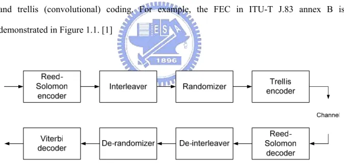
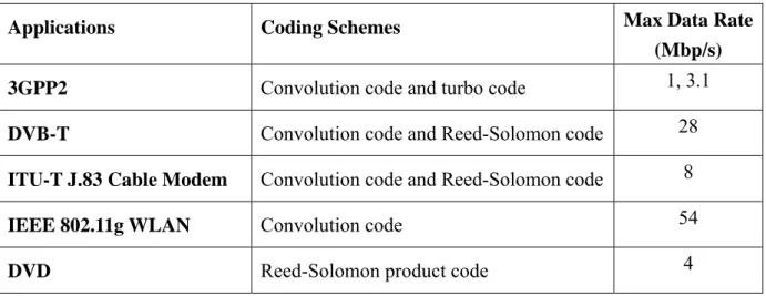
(11) Chapter 1 Introduction. 1.1. Motivation Forward error correction (FEC) is preservative in many digital communication and. storage systems for its feasibility between performance and complexity. FEC can be separated as four parts at many applications: randomization, Reed-Solomon (RS) coding, interleaving, and trellis (convolutional) coding. For example, the FEC in ITU-T J.83 annex B is demonstrated in Figure 1.1. [1]. Fig. 1.1: Layers of processing in the FEC from ITU-T J.83B Spec.. As listed in Table 1.1, many coding schemes have developed for different systems according to their essentials and channel characteristics. FEC can recover data from non-ideal channel effects such as thermal noise, interference, and fading. The performance strongly depends on the minimum free distance which is proportional to codeword length.. 1.
(12) Table 1.1: Difference of FEC specification between 3GPP and 3GPP2 standards. Max Data Rate (Mbp/s). Applications. Coding Schemes. 3GPP2. Convolution code and turbo code. DVB-T. Convolution code and Reed-Solomon code. 28. ITU-T J.83 Cable Modem. Convolution code and Reed-Solomon code. 8. IEEE 802.11g WLAN. Convolution code. 54. DVD. Reed-Solomon product code. 4. 1, 3.1. For maximum likelihood decoding, the complex algorithm requires massive computations and a large volume of memory accesses. The sub-optimal solutions are also computationally intensive. Hence most of the systems prefer dedicated hardware solution in terms of cost, power consumption and decoding speed. For different applications, FEC can be implemented by ASIC chips, reconfigurable ASIC chips, application specific digital signal processors (AS-DSP) and general purpose processors. ASIC chips have to be redesigned for different specification, which takes time and design effort. General purpose processors can realize various codes by software programming but will be uneconomic in power consumption and cost, especially for the wearable devices. A 16-bit AS-DSP is proposed here to provide a good tradeoff among flexibility, decoding speed and cost. Due to the special function units (FUs) and datapaths that accelerate most critical computations, most code designs can be implemented with better performance. The memory organization is also optimized to increase the bandwidth efficiency through vector operations which take advantages of the data locality. Optimizing the critical part in computations and memory accesses, the overall decoding speed can be enhanced with reasonable cost and power dissipation.. 2.
(13) 1.2. Thesis Organization The thesis will be organized as follows. In chapter 2, the algorithms of FEC are. introduced including convolutional codes and Reed-Solomon codes. Chapter 3 discusses the proposed AS-DSP including the instruction set and the hardware architecture. Chapter 4 details the applications of FEC decoding by proposed AS-DSP. The specifications of our implemented chip and comparisons with other similar works are also provided here. Finally, conclusion and future work are made in chapter 5.. 3.
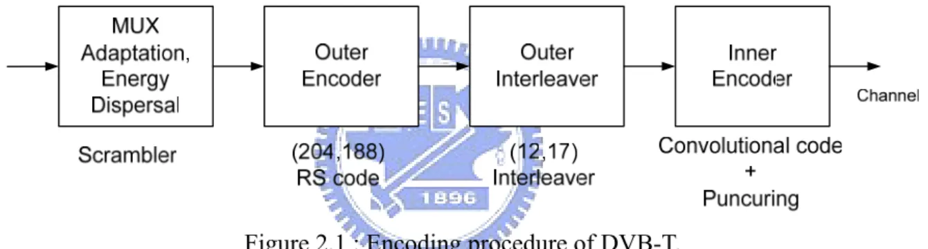
(14) Chapter 2 Overview of Forward Error Correction As mentioned in Figure 1.1, randomization and interleaving can be regarded as exchanging the data address. Figure 2.1 demonstrates the encoding flow of DVB-T, the encoding procedure also contains RS code and convolutional code. So the proposed AS-DSP concentrates at the RS coding and trellis coding parts. This chapter introduces the encoder and decoder for RS codes and convolutional codes.. Figure 2.1 : Encoding procedure of DVB-T.. 2.1. Introduction to Convolutional Code. An (N, K, M) convolutional code encodes K-bit message and outputs N-bit encoded data. It contains M bits memory and has K/N code rate. The Viterbi algorithm is a straightforward implementation of maximum likelihood (ML) decoding and is the most powerful and popular algorithm for decoding convolutional codes [2] [3]. For instance, the data of IEEE 802.11a has to be coded with a convolutional encoder of code rate 1/2, 2/3, or 3/4 corresponding to the desired data rate. The encoder has generator polynomials g0(x) = 1338 and g1(x) = 1718, of rate 1/2. Higher rates are drive from it by employing “puncturing”. Puncturing is a procedure 4.
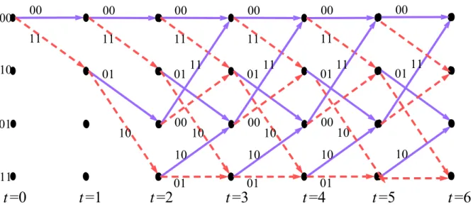
(15) for omitting some of the encoded data bits in the transmitter (thus increasing the coding rate) and inserting a dummy bit into the convolutional decoder on the receive side. Therefore, we concentrate at the 1/2 code rate of convolutional code.. 2.1.1. Convolutional Code Encoder. An example of (2, 1, 2) convolutional code is illustrated in Figure 2.2 (a). The generator polynomials g0(x) = 1112 and g1(x) = 1012. The convolutional encoder can be considered as a finite state machine (FSM) which has 2M states.. Figure 2.2 (a): (2, 1, 2) convolutional code encoder. (b): Finite state machine of (a).. Since the convolutional encoder is a FSM, Figure 2.2 (b) demonstrates the state diagram of Figure 2.2 (a). To encode input data, the convolutional encoder should be initialized with all-zero state by initializing the memory as zero. Then the state of Figure 2.2 (b) starts at state “00”. If the input data is 1, the next state will be “10” and the encoder outputs two bit (data A and data B) encoded data “11”. If the input data is 0, the next state will be “00” and the encoder outputs encoded data “00”. The encoding procedure with time indexes can be represented as trellis diagram. Figure 2.3 shows the trellis diagram of the encoder in Figure 2.2. 5.
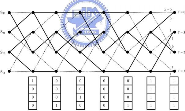
(16) 00. 00. 00. 00. 00. 00. 11. 11. 11. 11. 11. 01. 01. 10. 01. 00. 10. 11. t =0. t =1. t =2. 11. 01. 00. 10. 11. 10. 01. 00. 10. 10. 10. 01. 01. 01. t =3. t =4. 00. 11. 01. 11. 10 10. t =5. t =6. Figure 2.3 : Trellis diagram of (2, 1, 2) convolutional code encoder.. 2.1.2. Convolutional Code Decoder. At each time index, the decoder computes and compares the metrics of all branches that entering the state. The branch with the minimum metric and its corresponding decision bit will be preserved and others will be eliminated. The history record of the decision bits is called survivor. According to the minimum path metric (PM) at each time index, the maximum likelihood sequence can be estimated. The steps of Viterbi algorithm can be expressed as follow: 1.. Calculate the branch metrics between each state according to the received data.. 2.. Sum the previous PM ( Γ ) and corresponding branch metrics ( λ ) then compare the new PM with another that converges to the same state. The summation which has the smallest distance is updated as the new PM and the decision bit of selecting PM is stored into survivor memory. The operations above are called add-compare-select (ACS).. 3.. Decode the message sequence according to the minimum PM and the survivor memory (find the ML path). 6.
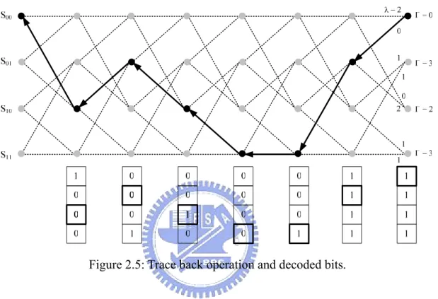
(17) In practice, the register exchange (RE) approach and trace back (TB) approach are useful methods for survivor path storage management in Viterbi decoder architecture. The RE costs great area and power dissipation but has less operation time. The TB approach is more suitable for DSP applications although it has the lower operation speed. The TB approach is a technique to trace the maximum likelihood sequence in the survivor memory. The convolutional code in Figure 2.2 is taken as an example. The trellis diagram and decision bit of each state is shown in Figure 2.4. In this figure, the point represents one state and the dotted line shows the eliminated path. At each state, if the ACS selects the upper sum (path), the decision bit will be “0”. Otherwise, if the ACS selects the lower sum (path), the decision bit will be “1”.. =2. S00. =0. 0 1. S01. =3 1 0. S10. 2. =2. 1. S11. =3. 1. 1. 0. 0. 0. 0. 1. 1. 0. 0. 0. 0. 0. 1. 1. 0. 0. 1. 0. 0. 1. 1. 0. 1. 0. 0. 1. 1. 1. Figure 2.4: Trellis diagram and decision bits of (2, 1, 2) convolutional code.. The path metrics accumulate in every time index and the minimum one indicates the maximum likely state. The corresponding sequence is the maximum likelihood sequence. The TB operation starts from the state of minimum PM and updates the state by shifting the state 7.
(18) left and replacing the lsb by the chosen decision bit. The TB operation of Figure 2.4 is demonstrated in Figure 2.5 and the decoded bits are the decision bit selected during TB operation.. Figure 2.5: Trace back operation and decoded bits.. Due to the supporting stage is quite large (up to 512 states) and TB approach has less address calculations, our proposed AS-DSP adopts the TB approach to increase the decoding performance.. 2.2. Introduction to Reed-Solomon Code RS codes are adopted in many communication and storage systems applications such as. digital TV system, cable modem, compact disk (CD), and digital versatile disk (DVD). Reed-Solomon (RS) codes have been widely used for error control due to its superior capability for bust error correction, the feasibility for VLSI implementation and the lower redundancy comparing with other FEC codes. A (N, K) RS code over GF(2m) contains N 8.
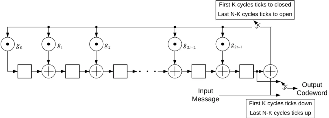
(19) symbols of codeword with K message symbols. The maximum correctable error number is t, t = ⎢⎣( N − K ) / 2 ⎥⎦ . The operations of RS codes are constructed by multiplication (FFM) and. finite field addition (FFA) over GF(2m). FFM takes many operation cycles in traditional DSP.. 2.2.1. Reed-Solomon Code Encoder. The message polynomial of RS has K symbols ( M K −1 , M K − 2 ," , M 0 ) and is expressed as follow:. M ( x) = M K −1 x K −1 + M K − 2 x K − 2 + " + M 0. (2. 1). Let α be a primitive element in GF (2m ) . The generator polynomial g ( x) of a t-error-correcting RS code has α , α 2 ," , α 2t as all its roots. It has degree of 2t and can be represented as follows:. g ( x) = ( x + α )( x + α 2 )" ( x + α 2t ) = g 0 + g1 x + " + g 2t −1 x2t −1 + x2t. (2. 2). Since α , α 2 ," , α 2t are roots of X q −1 − 1, q = 2m and g ( x) divides X q −1 − 1 . Therefore,. g ( x) generates a q-array cyclic code of length N = q − 1 with exactly 2t parity-check symbols. The encode process multiplies M(x) and X2t then divides the product by the generator polynomial to obtain a remainder polynomial r(x): M ( x) x 2t = q ( x) g ( x) + r ( x). (2. 3). r ( x) = r2t −1 x 2t −1 + r2t − 2 x 2t − 2 + " + r0. (2. 4). Where. The codeword polynomial C(x) with systematic form is: C ( x) = M ( x) x 2t + r ( x) = M K −1 x. K + 2 t −1. + " + M 0 x + r2t −1 x 2t. 2 t −1. + " + r0. (2. 5). The encoding of RS can be implemented by a systematic feedback shift register encoder 9.
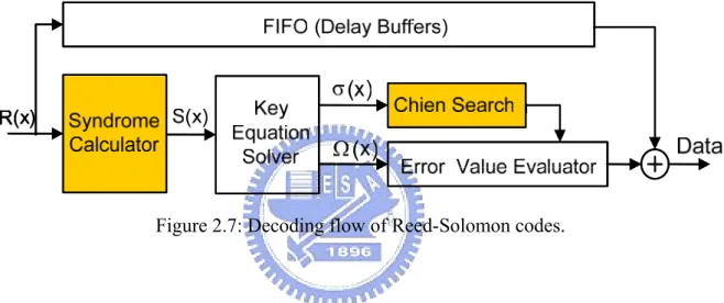
(20) as shown in Figure 2.6.. First K cycles ticks to closed Last N-K cycles ticks to open. g1. g0. g2. g 2t −2. g 2t −1. Input Message. Output Codeword First K cycles ticks down Last N-K cycles ticks up. Figure 2.6: Encoder of Reed-Solomon codes.. 2.2.2. Reed-Solomon Code Decoder. Assume the received polynomial is R(x) and the corresponding error polynomial is e(x). After translating, the received polynomial is:. R ( x ) = c ( x ) + e( x ). (2. 6). The error polynomial is: e( x ) = R ( x ) − c ( x ) = e1 x j1 + e2 x j2 + " + ev x jv , 0 ≤ v ≤ t , 0 ≤ j1 ≤ j2 ≤ " ≤ jv ≤ n − 1. (2. 7). where e1 , e2 ," , ev are error values and x j1 , x j2 ," , x jv are the error locations. Hence, we need to know the error locations x ji and the error values ei to determine e(x). The RS decoder can be separated into four parts as shown in Figure 2.7: 1.. Syndrome calculator. 2.. Key equation solver. 3.. Chien search. 4.. Error value evaluator 10.
(21) The syndrome calculator calculates the syndrome S1~S2t from received polynomial. The key equation solver generates the error locator polynomial σ ( x) and error value evaluator polynomial Ω( x) from syndrome. The error locations and error values are produced by Chien search and error value evaluator. We accelerate these operations by the vector instruction rssyn in AD-DSP since the syndrome calculator and Chien search operate regularly and determine the decoding speed. This will be discussed later.. Figure 2.7: Decoding flow of Reed-Solomon codes.. With Si = R(α i ) for 1 ≤ i ≤ 2t and R ( x) = c( x) + e( x) , the syndrome can be represented as: S1 = R(α ) = e(α ) = e1α j1 + e2α j2 + " + evα jv S 2 = R(α 2 ) = e(α 2 ) = e1α 2 j1 + e2α 2 j2 + " + evα 2 jv #. (2. 8). S 2t = R (α 2t ) = e(α 2t ) = e1α 2tj1 + e2α 2tj2 + " + evα 2tjv Then the syndrome polynomial is: S ( x) = S1 + S2 x + " + S2t x 2t −1. (2. 9). After syndrome calculator, the key equation solver has to find out the error locator polynomial σ ( x) and error evaluator polynomial Ω( x) . The key equation is defined as: 11.
(22) Ω( x) = S ( x)σ ( x) mod x 2t. (2. 10). The key equation can be solved by Euclidean algorithm [4] and Berlekamp-Massey algorithm [5]. The Euclidean algorithm requires many finite field divisions, leading to the reducing of decoding speed. Since the Euclidean algorithm makes the programming more difficult than BM algorithm does, the BM algorithm has been chosen to implement the RS decoder by AS-DSP. The inversionless Berlekamp-Massey algorithm [6] without erasure locator calculator which has 2t iterations is shown as follow: Initialization: Λ (b ) ( x) = 1, Λ ( a ) ( x) = 1, l = 0, k = 1, γ = 1. (2. 11). Computation: for (k = 1; k ≤ 2t ; k + + ){ Λ ( a ) ( x ) = xΛ ( a ) ( x ) l. δ = ∑ Λ j (b ) Sk − j j =0. Λ ( c ) ( x) = γΛ ( b ) ( x) + δΛ ( a ) ( x) If (δ ≠ 0 and 2l ≤ k − 1){. (2. 12). Λ ( a ) ( x) = Λ ( b ) ( x), l = k − l , γ = δ } Λ (b ) ( x) = Λ ( c ) ( x) }. The element δ is the discrepancy which is the convolution of syndrome polynomial and error locator polynomial. The dummy discrepancy γ keeps the value of previous non-zero discrepancy.. The discrepancy is used to verify that the linear feedback shift. register generates corresponding syndrome sequence at each step. If the discrepancy is equal to zero, the error locator polynomial and the dummy discrepancy remain. After the computation above, the polynomial Λ ( c ) ( x) is equal to σ ( x) . The Chien search 12.
(23) can find out the roots of σ ( x) which are the error location numbers. The methodology of Chien search is substitution of error locator polynomial with finite field elements to find out the roots of σ ( x) . k =0 if (σ (α −1 ) == 0){. βk = α i , k + +. (2. 13). }. According to the Forney algorithm [7], the error value δ k at location β k is given by. δk =. −Ω( β k−1 ) σ ' ( β k−1 ). (2. 14). Where. σ ' ( x) =. d d v σ ( x) = ∏ (1 − β i x) dx dx i =1 v. = −∑ β l l =1. v. ∏ (1 − β x). i =1,i ≠ l. (2. 15). i. And Ω( x) = S1 + ( S 2 + σ 1S1 ) x + ( S3 + σ 1S 2 + σ 2 S1 ) x 2 + " + ( Sv + σ 1Sv −1 + " + σ v −1S1 ) x v −1. 2.2.3. (2. 16). Montgomery Multiplication Algorithm. An element of the field GF(pm) with a prime p can be interpreted as the polynomial representation.. The polynomial multiplication in GF(pm) corresponds to the multiplication. of polynomials modulo an irreducible polynomial of degree m. Suppose A and B are two elements in GF(pm), and µ(x) is the corresponding irreducible polynomial of degree m. By the polynomial representation, the multiplicative operation C=AB can be expressed as follows:. C ( x) = A( x) B( x) mod µ ( x) Where C is also an element of GF(pm). 13. (2. 17).
(24) Actually, the finite field addition and subtraction are just XOR operations. Therefore, what we interest is the multiplication and division (or say, the inverse operation) in finite field. According to the modulo operations in (2.17), we can adopt Montgomery multiplication algorithm to calculate the product C(x). The Montgomery multiplication algorithm has been proven that this algorithm can replace the modular operation with a series multiplication. The following equation defines the Montgomery product of A and B:. Cˆ ( x) = A( x) B( x) R * ( x) mod µ ( x). (2. 18). The polynomial R*(x) here is a fixed element of GF(pm) satisfying R(x)R*(x) =1 mod µ(x) while R(x)=xm. Note that R(x) and µ(x) must be mutually prime. It has been proven by [8] that the result Cˆ ( x) of (2.18) can be obtained by following equations:. Q( x) = A( x) B( x) µ * ( x) mod R( x). (2. 19). Cˆ ( x ) = [ A( x ) B ( x ) + Q ( x ) µ ( x )] / R ( x ). (2. 20). The polynomial µ*(x) in (2.19) is defined as µ(x)µ*(x)=1 mod R(x). As compared with (2.18), it is evident that modulo µ(x) operation is replaced by modulo R(x) and division by R(x) operations. Since R(x)=xm, implementation of (2.19) and (2.20) are much easier than that of (2.18). Furthermore, as A is interpreted in polynomial form and R*(x)= x-m mod µ(x), (2.18) can be rewritten as:. Cˆ ( x) = [am−1 B( x) x −1 mod µ ( x)] + [am−2 B( x) x −2 mod µ ( x)] + ... + [a 0 B( x) x −m mod µ ( x)]. (2. 21). Rearrange this equation, an iterative representation comes out:. Cˆ ( x ) = [ a m −1 B ( x ) + [..[ a1 B ( x ) + [ a 0 B ( x ) x −1 mod µ ( x )]] x −1 mod µ ( x )]...] x −1 mod µ ( x ). (2. 22). Based on this equation and the transformation from (2.20) to (2.22), the Montgomery 14.
(25) multiplication algorithm is derived as:. Montgomery multiplication algorithm. S0 ( x) = 0; for (i = 0; i < m; i + +){. ρi ( x) = [( Si ( x) + ai B( x)) µ * ( x)] mod x; Si+1 ( x) = [ Si ( x) + ai B( x) + ρ i ( x) µ ( x)] / x;. (2. 23). } Cˆ ( x) = S m ( x); The term µ*(x) is the multiplicative inverse of µ(x) under modulo x multiplication. In GF(2m), elements are often represented in binary digits, and the coefficients ai are referred to the bits of A. The binary representation will cause some reductions to Montgomery multiplication algorithm. Since µ(x) is irreducible, the results of µ(x) mod x and µ*(x) mod x are both equal to 1. The µ*(x) term in the Montgomery multiplication algorithm can be eliminated, which leads ρi(x) to equal the least significant bit of the sum Si(x)+ aiB(x). The number of recursive operation in Montgomery multiplication depends on the field degree m. However, some modification can be proposed to remove the effect of unexpected variable m.. In equation (2.19) and (2.20), R(x) is modified to be Rd(x)=xd, and d is a. constant integer such that d≧m. Since the result of R*d(x) mod µ(x) is an element of GF(pm), there exists an element R*d(x) in the field GF(pm) that satisfies Rd(x)R*d(x)=1 mod x. Therefore, the modified Montgomery multiplication (MM) algorithm for GF(2m) with m≦d is constructed:. Modified Montgomery multiplication algorithm 15.
(26) MM ( A( x), B( x), µ ( x)){ S 0 ( x) = 0; for (i = 0; i < d ; i + +){ if (i ≥ m) ai = 0; T ( x) = S i ( x) + ai B( x);. (2. 24). S i +1 ( x) = [T ( x) + t 0 µ ( x)] / x; } Cˆ ( x) = S d ( x); }. The term t0 is the least significant bit of the temporal element T(x). If the field degree is less than d, the most significant bits of A is set to zero .The final result will be multiplying the normal finite field product A(x)B(x) by a constant element R*d(x) of GF(2m). The output of Montgomery multiplier involves a constant factor R*d(x) mod µ(x) with the standard product. Such constant factor can be canceled by applying one additional Montgomery multiplier. Calculation of the product C(x)=A(x)B(x) can be expressed as:. K ( x) = x 2 d mod µ ( x) Cˆ ( x ) = MM ( A( x ), B ( x ), µ ( x )) C ( x ) = MM (Cˆ ( x ), K ( x ), µ ( x )) where K(x) is treated as a constant value for a given µ(x).. 16. (2. 25) (2. 26) (2. 27).
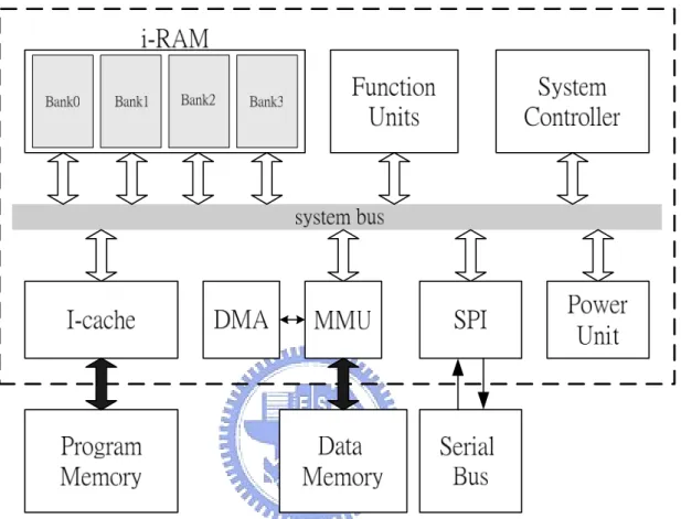
(27) Chapter 3 Proposed AS-DSP Architecture Since the channel decoding algorithms induce large memory bandwidth requirement and many computationally intensive operations, they become the critical parts of system throughput in general digital signal processors (DSPs). The operations such as finite field multiplication (FFM) and finite field inversion (FFI) also require many instruction cycles for conventional DSPs. Besides, the complex datapaths and data control degrade the performance and make programming of channel decoding more difficult. Special FUs are used in the proposed architecture to accelerate the decoding speed. The decoding algorithm can be efficiently implemented with higher throughput and less program size as a result of the proposed datapaths and data flow control. Moreover, the programs written in vector instructions are suitable for almost specifications for the same decoding scheme by adjusting the coefficients. Thus, programming in vector instructions is efficient and reusable.. 3.1. 6-Staged Pipeline Architecture. Figure 3.1 shows the block diagram of the processor. System controller manages the pipeline flow, FUs and access of internal memories (i-RAM). The power saving controller, power unit, is also designed to reduce power consumption by means of closing components without operation. The external memories including program memory and data memory are controlled by instruction cache (I-cache) and memory management unit (MMU), respectively. Note that a direct memory access (DMA) controller is used to improve the performance of data memory. Furthermore, considering the link with other devices, we added a serial 17.
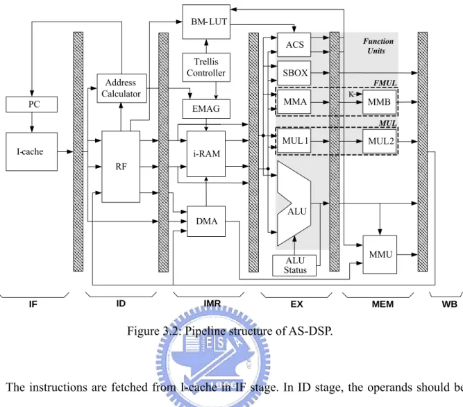
(28) peripheral interface (SPI) as a serial interface connecting to external serial bus. The hardware architecture will be introduced in this section.. Figure 3.1: Block diagram of AS-DSP.. As shown in Figure 3.2, the processor has 6 pipeline stages: instruction fetch (IF), instruction decode (ID), i-RAM read (IMR), execution (EX), data memory access (MEM), and write back (WB).. 18.
(29) BM- LUT Function Units. ACS. Address Calculator PC. Trellis Controller. SBOX FMUL. MMA. EMAG. K. MMB MUL. MUL1 I-cache. MUL2. i-RAM RF. ALU. DMA. ALU Status. ID. IF. IMR. EX. MMU. MEM. WB. Figure 3.2: Pipeline structure of AS-DSP.. The instructions are fetched from I-cache in IF stage. In ID stage, the operands should be read from register file (RF) that is composed of 32 general purpose registers. IMR stage has four 256x16-bit embedded SRAMs controlled by embedded memory address generator (EMAG). The addresses of each SRAM are generated according to instructions, SPRs, and system controllers. EX stage contains several FUs: ACS, SBOX, finite field multiplier (FMUL), 32-bit arithmetic multiplier (MUL), and arithmetic logic unit (ALU). To increase throughput, FMUL is divided into MMA and MMB whereas MUL is pipelined to MUL1 and MUL2.. The data from external memories will be accessed in MEM stage with access time. determined by SPRs. The results should be written back to RF and i-RAM in WB stage.. System Controller. Since the AS-DSP is a pipelined architecture and the executed instructions might have 19.
(30) the data dependency. The system controller detects the dependencies and either stalls the operations or forwards the dependent data. Figure 3.3 is the timing graph of several instructions with data dependency to Ins 1. The dotted lines represent the data path that need be executed and the black line is the forwarding path.. Figure 3.3: Pipeline forwarding of AS-DSP.. The system controller also manages the configuration of FUs for different datapaths and applications according to the instructions and SPRs. For instance, system controller can change the finite field number for rssyn instruction base on the GPRs, r47[5]. To get the higher through, system controller enable the other two finite field multipliers and open the datapath for them.. Instruction Cache (I-Cache). Cache technology is used for almost every processor to improve system performance by reducing the external memory accessing. Because of the spatial locality of programs, 20.
(31) instruction cache can significantly diminish the load operation from program memory especially when the loop condition occurred. Consider area and speed, the instruction cache (I-Cache) of AS-DSP has 128 entries for 16-bit width; it based on two-set-associative scheme as shown in Figure 3.4.. Figure 3.4: Structure of I-Cache.. The miss penalty of I-Cache is five cycles because the latency of access external program memory. Table 3.1 lists the simulation result of I-cache when decoding a period of 64 states convolutional code using Viterbi algorithm. The program can decode 40 bits which calculates 80 period of trellis and traces back 40 times.. Table 3.1 Simulation result of I-Cache.. 21.
(32) Number of instructions. 120. Number of executing instructions. 2537. Number of hit instructions. 2400. Hit rate. 94.6. Average cycle per instruction (CPI). 1.216. Serial Peripheral Interface (SPI). Since the interface to communicate with other system is needed and the data rate of FEC decoding is not too high, the proposed AS-DSP uses a serial interface SPI. The block diagram of SPI is shown in Figure 3.5.. Figure 3.5: Block diagram of SPI. 22.
(33) The SPI module allows a duplex, synchronous, serial communication between the MCU and peripheral devices. It has these distinctive features as fellow: z. Master mode and slave mode. z. Bi-directional mode. z. Slave select output. z. Double buffered data register. z. Serial clock with programmable polarity and phase. According to the document, the maximum transmission rate is 1/2 clock rate. For example, the maximum data rate of SPI is 66.5Mbp/s if the operating frequency is 133MHz.. 3.2. Instruction Set & Register File The instruction set of proposed processor is listed in Table 3.2. The general instructions. support the basic functions such as arithmetic operations, logical operations, and finite field multiplication. They also control the programs by register transfer, load/store, and branch instructions. Note that the special instruction for advance encryption standard (AES) is a hardware lookup table called SBOX in its algorithm [9]. The Viterbi result instructions output the decoded data to external memory or to the serial bus. The vector instructions have six kinds of operations including two kinds for FEC applications and they will be discussed later.. Table 3.2 Instruction Set of AS-DSP General Instructions Arithmetic. add, sub, addi, subi, add32, sub32, shift, arishift, mul, mac, mac32. Logic. And, or, xor, not, inv. AES. sbox, sboxi. Finite field multiplication fmul 23.
(34) Register transfer. move, movie, set. Branch. Jump, jumpi, beq, beqi, bne, bnei, call, return, loop,. Load/store. Load, store. Viterbi result. viso, vistore Vector Instructions. Arithmetic. vaddv, vsubv, vaddr, vsubr, vmac, vmin, vmax, vmulv. Logic. vandv, vorv, vxorv, vnot,. Load/store. vpload, vnload, vostore, vnstore. Finite field multiplication. vfmac, vfmulv. Viterbi. viacs, viacsm, vitb. RS. rssyn. The general instructions have three addressing modes (a), (b) and (c). The Rd, Rs1, Rs2 represent destination Register, source register 1 and source register 2, respectively. The operation of each addressing mode is decided by the field “OP code” and “Func”.. Addressing mode (a), Rd = operation ( Rs1, Rs 2) 15. 12. 11. OP code. 9. 8. Rd. 6. 5. Rs1. 2. 1. Rs2. 0. Func. Addressing mode (b), Rd = operation ( Rd , constant) 15. 12. 11. OP code. 9. 8. 1. Rd. Constant. 0 Func. Addressing mode (c), Rd = operation (constant) 15. 12 OP code. 11. 1 Constant. 24. 0 Func.
(35) The vector instructions have two addressing mode (d) and (e). The Vd, Vs1, Vs2 represent destination vector, source vector 1 and source vector 2, respectively. Addressing mode (d) is designed for vector memory access and (e) is the vector operations. Section 3.4 details the vector operations and gives some examples to show how the vector operations work.. Addressing mode (d), Vd [i % 256] = operation (data _ memory[i + Rs1]), i ∈ ( R32 + 0) ~ ( R32 + Rs 2 − 1) 15. 12 OP code. 11. 10 9. Reserved. 8. 6. Vd. 5. 2 1. Rs1. Rs2. 0 Func. Addressing mode (e), Vd [i % 256] = operation (Vs1[i ],Vs 2[i ]), i ∈ ( R32 + 0 ~ R32 + Rs 2 − 1) 15. 12 OP code. 11. 10. Vd or Rd. 9. 8 Vs1. 7. 6 5. Vs2 or Rs1. 2 Rs2. 1. 0 Func. The register file (RF) composes 32 general purpose registers (GPRs) and 16 special purpose registers (SPRs). The functions of RF are listed at Table 3.3 and Table 3.4. The contents of SPRs configure the Function units, i-RAM, datapaths, and status of processor. SPRs are only writable for programmers by using register transfer instruction, “set”.. Table 3.3 General purposed registers of AS_DSP GPRs. r0~r13. GPRs. r14. GPRs, (vmin, vmax index register). r15. GPRs, (mul result [31:16]). r16. GPRs. 25.
(36) r17 r18~r27. GPRs , (compare register of beqi, bnei) GPRs. r28. GPRs , (result of rssyn {S3,S2}). r29. GPRs , (pointer of survival memory). r30. GPRs , (pointer of trace back). r31. Zero. Table 3.4 Special purposed registers of AS_DSP r32. i-RAM starting address. r33. g1(x) of convolutional code [8:0]. r34. g2(x) of convolutional code [8:0]. r35. Viterbi constraint length. r36. Pm00. r37. Pm01. r38. Pm10. r39. Pm11. r40. k(x) of Montgomery mul, [7:0]. r41. k(x) of Montgomery mul, [7:0]. r42. The register of jump. r43. Loop size. r44. Trace back length. r45. RS alpha 1. r46. RS alpha 2. r47. Processor status control register. SPRs. 26.
(37) The SPR R47 controls the statuses of processor such as I-cache, cycles of accessing external memory and decoding method for FEC applications. The detail functionality of R47 is shown at Table 3.5.. Table 3.5 Functionality of SPR R47 0: use min pm to trace back r47[0]. Trace back control 1: use max pm to trace back 0: use 8-bit, [7:0]. r47[1]. RS data type 1: use 16-bit, [15:0] 0: decode 1-bit/vitb. r47[2]. Trace back method 1: decode N-bit/vitb 0: R28=R28. r47[3]. Read serial in data 1: R28=serial input data Finite field multiplier status for 0: use 1 stage of FMUL. r47[4] rssyn instruction. 1: use 2 stage of FMUL. Finite field multiplier number 0: use 2 FMULs r47[5] r47[11:6]. for rssyn instruction. 1: use 4 FMULs. Reserved. Reserved 0: Off. r47[12]. Cache enable 1: On. r47[15:13]. Data memory access cycle. 0: 1 cycle per fetch # 7: 8 cycles per fetch. In order to control the serial interface SPI, the virtual register is designed to index the SPCR, SPSR, SPDR, and SPER [11]. Actually, the register SPDR is the index for two FIFO 27.
(38) buffer; input buffer and output buffer. The corresponding virtual registers for SPI are listed at Table 3.6.. Table 3.6 Virtual registers of AS-DSP r48. SPI control register, SPCR. r49. SPI status register, SPSR. r50. SPI data register, SPDR (serial output data register). r51. SPI extension register, SPER. r52~r53. Reserved SPI data register, SPDR (write dummy data to fetch. r54 serial input data) r55. 3.3. Reserved. Function Units Function units of AS-DSP include ACS, SBOX, arithmetic multiplier (MUL), and finite. field multiplier (FMUL). The ACS unit is used to speed up the operation of Viterbi decoding. SBOX is the nonlinear substitution of AES which is usually designed as a ROM or lookup table. The SBOX block in processor is implemented by composite field [10] and saves 20% area as compared with ROM. The processor contains a 16-bit natural number multiplier which can perform 32-bit result. The multiplier is pipelined as two stages (MUL1 and MUL2) to increase operating speed.. 3.3.1. ACS. Add-compare-select (ACS) calculates sums of path metrics and branch metrics then 28.
(39) compare them to select a probable decision. Figure 3.6 represents a period of 4 states convolutional code. There are two butterflies in one transition in Figure 3.6, and each one has two ACS operations.. Figure 3.6: Transition of convolution code.. The function unit ACS is composed of four adders and two comparators as shown in Figure 3.7, and therefore it provides two ACS operations per cycle.. Figure 3.7: The function unit ACS. 29.
(40) 3.3.2. Finite field multiplier. The Montgomery algorithm provides a universal and simple modular operation. Montgomery multiplication (MM) function is used to implement multiplication of A and B in finite field GF (2m ) as (1). In (2), another MM block is used to normalize (1) by multiplying a constant K, or the inverse of K*. The m of FMUL is small than or equal to 8, and µ is primitive polynomial.. Cˆ = A × B × K * mod µ. (3. 1). C = A × B mod µ. (3. 2). MMA and MMB are the same function blocks in Figure 3.8. Both of them contain two 8-bit (m≦8) Montgomery multipliers (MM), one is for bit 7~0 and another is for bit 15~8. The block diagram of FMUL is shown in Figure 3.8 (a). In order to reach the higher operation speed, the FMUL is pipelined to two stages as shown in Figure 3.8 (b).. MMA. MMB. MM. MM. C1. MM. C0. A1. A B. MM A. ∧. C K. B1. MM B. K. C. A0. µ. MM B0. K. (a). (b). Figure 3.8 (a): Block diagram of finite field multipliers. (b): Datapath of two 8-bit finite field multipliers. 30.
(41) 3.4. Vector Instructions Most of decoding algorithms involve sequentially operations on a series of data. The. regularity of computation will simplify the memory access and data flow control. To efficiently process such operations, the vector instructions have been included in the processor. These instructions benefit many computations such as syndrome calculation in RS decoding and ACS operations in Viterbi decoding. The vector operations require multiple accesses of i-RAM and configuration of datapaths. EMAG calculates the appropriate addresses for vector operations to simplify the executions. Furthermore, the automatic control of operations improves both the throughput and the size of programs.. 3.4.1. Vector instruction for general applications. The general applications include arithmetic, logic, load/store, and finite field multiplication. Vector instructions of the AS-DSP are listed in Table 3.2. The character “V” means vector and “R” represents register. For instance, the instruction “vaddv e2 e1 e0 r7;” expresses vector1 (embedded memory 1) adds vector0 then stores the results to vector2. It can be denoted as e2 [i ] = e1[i ] + e0 [i], i ∈ (r 32) ~ (r 32 + r 7 − 1) mod 256 . The register r32 is the initial index of vector operations. Because the memory of i-RAM has 256 entries, the register r32 and r7 here must less than or equal to 256. Table 3.7 takes some vector instructions as examples and explains their functions.. Table 3.7 Examples of vector instruction for general application. Kind. Instruction. Arithmetic vaddv e2 e1 e0 r7;. Function. Index i*. e2[i] =e1[i]+e0[i]. r32~r32+r7-1. 31. Index j. N.A..
(42) vaddvre2 e1 r0 r7;. e2[i] =e1[i]+r0. r32~r32+r7-1. N.A.. r32~r32+r7-1. N.A.. r3 =max(e0[i]) vmax r3 e0 r7; r14=i, e0[i]=max vpload e1 r6 r7;. e0[i]=memory[j]. r32~r32+r7-1. r6~r6+r7-1. vnload e1 r6 r7;. e0[i]=memory[j]. r32~r32-r7+1. r6~r6+r7-1. Load/store *: i = i mod 256 when it is bigger than 256.. Figure 3.9 represents the vector operations of arithmetic, logic, and finite field multiplication. The EMAG generates the addresses and controls the read/write operation for 4 banks of i-RAM due to different instructions; it also manages the selector to choose the appropriate data to support two read and two write at most in one cycle.. Figure 3.9: Block diagram of vector operations.. The load/store of vector operations is moving a serial of data from/to the external data memory. Because the data is continue, the processor can only calculate the initial address and access data serially. Thus, the DMA technology is used to automatically access data for i-RAM. In order to reduce idle cycles when accessing a block of data from external memory, 32.
(43) the memory accesses and other operations are designed to execute simultaneously. Hence the AS-DSP can be used efficiently. Table 3.8 shows the operations of syndrome calculation with and without DMA. With out DMA, the AS-DSP loads the received polynomial to i-RAM than calculate the syndrome and takes N +. N *t cycles. With DMA, the received Number of FMUL. polynomial can be loaded when calculating last syndrome and takes only. N *t Number of FMUL. cycles.. Table 3.8 Cycles of calculating syndrome with and without DMA (204,188)RS syndrome calculation (cycle) 2 FMUL. 1020. 816. 4 FMUL. 612. 408. AS-DSP. The instruction and addressing mode (d) of load/store for vector operations are mentioned in section 3.1. Figure 3.10 is the block diagram of DMA. FIFO buffer stores the information for DMA form the instruction as follows. z. Values of Rs1[15:0], Rs2[7:0] and r32[7:0].. z. L/S, P/N decoded from OP code and Func.. z. Vd, Rs1 and Rs2. The index Vd, Rs1 and Rs2 of each DMA access will be compared by system controller.. The DMA stall signal will be assert if there is any dependence between vector memory access and others. The controller in DMA asserts the Buffer Full signal if the FIFO Buffer is full then the system controller will stall the processor.. 33.
(44) FIFO Buffer r32 Rs1 Rs2 8. / 2. /. /. / 1. Buffer Full. / 11 /. 16. 1. controller DMA stall. 8. /. L/S Vd P/N. /. Buffer pointer. 8. Address Calculator. / 16. Enable. Enable & Read/write signal. address. L/S. Bank0. Data0. Bank1. Data1. Address. Bank2. Data2. Bank3. Data3. Selector. EMAG. 16-bit address. Data out / 16. MMU. / 16. Data in. External Data Memory. 16-bit data bus. i-RAM. Figure 3.10: Block diagram of DMA.. 3.4.2. Vector instruction for FEC applications. In this section, the vector instruction for Reed-Solomon (RS) and Viterbi decoding are introduced here.. 3.4.2.1.. Viterbi Decoding. The Viterbi algorithm [12] consists of three parts: branch metric calculation (BM), add-compare-selection (ACS), and survival memory (SM). In BM, the DSP will calculate branch metrics for each state transition in the trellis. Since branch metrics have only four different values in 1/2 code rate convolutional code, the Branch metric look-up-table (BM-LUT) approach is proposed to reduce unnecessary calculations.. 34.
(45) Output Data A Next State Input Data Current State Output Data B Figure 3.11: Encoder of 64 state convolution code.. The branch metric are the encode results of convolutional code and convolutional encoder can be regarded as a finite state machine as shown in Figure 3.11. So the BM-LUT can calculate the branch metric by the state transitions and the generator polynomial. The architecture of BM-LUT is illustrated in Figure 3.12. The constraint length and generator polynomial decides the input of modulo-two adder. The outputs of modulo-two adder control the multiplex, MUX and select branch metric form pm00~pm11 which are the values of four different branch metric.. G1(x) (r33) \ 9. G2(x) r34. \ 9. \ 1. \ 9. \ 1. pm00 (r36). Current State \ 8 Next State \ Constraint 8. pm01 (r37) pm10 (r38). M U X. BM. pm11 (r39). length (r35). Figure 3.12: Architecture of BM-LUT.. The vector ACS operation performs two ACS operations according to the BM-LUT and 35.
(46) saves the decisions to external memory. For instance, the instruction “viacs e2 e0 e1 r7” represents one vector ACS operation in Figure 3.13. Bank0 and Bank1 store the path metric and their indexes are the current states. The trellis controller generates the address of Bank0~Bank3 which are the current states and next states in Figure 3.13.. Figure 3.13: ACS vector operations diagram.. Figure 3.14 represents the architecture of vector ACS instruction. The trellis controller generates read and write addresses which are the current and next state. The BM-LUT calculates branch metric for each ACS then ACS Unit computes the new path metric and store them to Bank2 and Bank3 in this case. The decisions during ACS operation are buffered and stored into the external memory. The GPRs r29 which is the stack pointer of survival memory are automatically update when the decisions are stored.. 36.
(47) Trellis Controller. BMLUT 16-bit Stack Buffer. ACS Unit BM0. Bank0. C M P. PM0j. Decision0 1. PM1j BM1. M U X. Bank1 Bank2. BM2. C M P. Bank3 BM3. PM0j+1. Decision1 1. M U X. D D D D 16 \. D D. External Mmory. PM1j+1. Figure 3.14: Architecture of vector ACS instruction.. After the last ACS operation, the most probable state is decided by the minimum or maximum path metric. Trace back operation is used for SM, and the survival path can be found through external memory accesses.. 3.4.2.2.. RS Decoding. The syndrome calculator and Chien search constitute over 50% computations of RS decoding, and both of them are similar operations [13]. The syndrome calculator generates a set of syndromes S1~S2t from received polynomial R(x). The representation of syndromes calculation is as following. The received polynomial can be written as (3.5) by Horner’s rule. Si = R(α − i ), i ∈1 ~ 2t N −1. R( x) = ∑ R j x j = R0 + R1 x + R2 x 2 + " + RN −1 x N −1 j =0. 37. (3. 3) (3. 4).
(48) N −1. R ( x) = ∑ R j x j = ((( RN −1 x + RN − 2 ) x + RN −3 ) x + " + R0 ). (3. 5). j =0. The Montgomery multiplier of R j and α − j can be written as (3.6) according (), and the result should be normalized by MMB as Figure 3.8 (a). Function (3.6) can be represented as (3.7) if α − j is replaced by α − j + m to avoid normalizing K*. Without normalization, multiplications in syndrome calculation can be executed by a single MM block, MMA or MMB. Cˆ ( x) = α −i R jα − m mod µ ( x), K * = α − m. (3. 6). Cˆ ( x) = α −i + m R jα − m mod µ ( x). (3. 7). = α − i R j mod µ ( x). Because α −1 ~ α −2t and α −1+ m ~ α −2t + m are constants and m is fixed, the replacement requires no extra computations. Each MM block can calculates one syndrome itself, and therefore the execution time in syndrome calculating is two time faster than traditional works.. α−j. α−j. 1. 16 \. 8 \. 8 \. 3. MM. S1. 0. 0. 1. 1. α−j. S3. MM. S2. α−j. 0. iRAM. MM. 2. MM. S0. 0. 0. 1. 1. 38.
(49) Figure 3.15: Datapath of FMUL when calculating syndrome.. Figure 3.8 (b) is the datapath of calculating finite field multiplication and Figure 3.15 is the datapath when calculating syndrome. The register r45[15:8], r45[7:0], r46[15:8] and r46[7:0] represent constants α − j0 , α − j1 , α − j2 and α − j3 ,respectively. For example, the instruction “rssyn r0 e0 r7;” represents syndrome calculation. The receive polynomial has to be stored in Bank0 and r7 must equals to N. The final results S0 and S1 will write back to register r0 according to the instruction. Furthermore, the results S2 and S3 will write back to the register r28 as shown in Table 3.3. At the first cycle, the multiplexers in Figure 3.15 select the input from iRAM by setting control signal to zero. Then the function block MM calculates the product of RN −1α − ji , i ∈ 0 ~ 3 ( rN −1 is the first output of iRAM). At the second cycle, the value of modulo-2 adders can be represented as Si = RN −1α − ji + RN − 2 , i ∈ 0 ~ 3 . The multiplexers selects the values S0~S3 after the first cycle. The syndrome S0~S3 will be calculated after N cycles. Two 8-bit FFM are implemented in this design. Because of the designed datapaths, FFM can be easily added according to the applications, and calculation speed will rise linearly.. 39.
(50) Chapter 4 Chip Implementation & FEC Applications. This chapter discusses the details of implement RS decoding and Viterbi decoding by AS-DSP. Before the discussion, the design flow will be introduced. The Design flow chart is illustrated in Figure 4.1.. Figure 4.1: Design flow chart. 40.
(51) At first, we simulate the FEC algorithm by software (C or Matlab) and record the results for each decoding steps. After finishing the assembly codes, the translator translates them to machine codes. To ensure the accuracy of the assembly codes and machine codes, the simulator compares the machine codes with assembly codes. Besides, the simulator can calculate the values of every register, i-RAM and external memory for each instruction and represent them if user wants. After comparing with the results of software and simulator, the machine codes will be test in the pre-layout simulation of AS-DSP. If the comparison is not correct, we need to check out the RTL coding until.. 4.1. Viterbi decoding using AS-DSP. 4.1.1. Some details in Viterbi decoding. In section 2.1.2, we introduced the Viterbi decoder and explain why we select the TM approach. Here we discuss other issues in Viterbi decoding. In the real applications, the length of received symbols may be quite long. It is impossible to store the decision bits if we start to trace back after received all symbols. Thus, a suitable TB length (or called truncation length) should be defined without serious performance degradation. The rule of thumb is that truncation length is about five times of constraint length. In Viterbi algorithm, the path metric accumulates at each time index; and undoubtedly increasing as time goes by. The path metric must be limited in a range so that it can be expressed with finite bits. There are several approaches such as reset, rescaling subtraction, shift, and modulo normalization. The modulo normalization approach (also called two’s complement arithmetic approach) is more efficient than others. As shown in Figure 4.2, the maximum difference between time constant t=k and t=2k-L is B x L; where B and L are maximum value of branch metrics and truncation length, respectively. 41.
(52) Figure 4.2: The survival path of convolutional codes.. The concept of modulo normalization is not to avoid overflow but to accommodate. Figure 4.3 demonstrates the ideal of modulo normalization. M1 and M2 are both positive number and M 1 − M 2 < 2c −1 ; where C is the bit number representing path metric. m1 = M 1 mod 2c m2 = M 2 mod 2. (4. 1) c. Thus, m1 and m2 can be presented on half cycle without confusing their difference. The penalty of modulo normalization is to increase one bit [14].. Figure 4.3: The ideal of modulo normalization. 42.
(53) The AS-DSP has 16-bit data type, which means it can tolerate the maximum difference about 215-1. The huge range of path metric can implement every spec. of convolutional code without error when normalizing. As shown in Figure 4.2, the truncation length is L. It means that the decoded data has the acceptable accuracy if we track back at least L length then decode the data. The AS-DSP has two decoding strategies for different decoding speed. Strategy one is decoding one bit data after tracing back L length and Strategy two is decoding k bits data. Take Figure 4.2 as example. Since we can ensure the accuracy before time index k, we can trace back form time index t = 2k to t = 0. Then the data form 0~k can be decoded and the decoding speed is k times as fast as strategy one.. 4.1.2. Decoding procedure and data rate for Viterbi decoding. This section talks about the notice of Viterbi decoding using AS-DSP and takes the convolutional code of 802.11a as an example. The following steps are the decoding procedure of Viterbi decoding: 1.. Initializing the AS-DSP. The FUs and states of processor should be initialized by setting the SPR r47. The. detail of r47 is listed in Table 3.2. For this example, we enable the cache and set the access cycle as 3 (base on the spec. of asynchronous RAM [15]). Table 4.1 lists the fields that need to be initialized.. Table 4.1 The list of initialization. SPR. Value. r47[0]. 0. Function Use min PM to trace back. 43.
(54) 2.. r47[2]. 1. Decode N-bit/vitb N=trace back length. r47[12]. 1. Enable the I-Cache. r47[15:13]. 2. 3 cycles for accessing external memory. Setting the coefficient of Viterbi decoding In this step, we setup the coefficient of Viterbi decoding. First, we set the trace back. control and trace back method as “1”. The trace back control is to find the maximum likelihood path by selecting the minimum or maximum path metric according to different applications. The trace back method was talked before; it can decode k bit data when it setting as 1. Second, we setup the generator polynomial g1(x) and g2(x), constraint length and trace back length. The PMs stored in i-RAM have to be initialized, too. Tables 4.2 lists the coefficient and explain their function.. Table 4.2 The coefficient of Viterbi decoding.. 3.. GPR. Value. Function. r29. 2000hex. Pointer of survival memory. r33. 1338. Generator polynomial g1(x). r34. 1718. Generator polynomial g2(x). r35. 7. Constraint length. r44. 40. Trace back length (truncation length). Execute ACS operations. After initializing the AS-DSP and setting the coefficient, we start the Viterbi. decoding. The first step of ACS operation is to calculate the branch metrics 44.
(55) (pm00~pm11). After that, the instruction viacs updates the new PMs, survival memory and pointer of survival memory automatically.. 4.. Trace back operation. The instruction vitb can trace back according the minimum PM then decode the. information data. Since we set the trace back method as “1” and the track back length is 40. We get 40 information bits after 80 (40 x 2) memory accessing. Thus, it takes 2 x L cycles for generating one information bit in vitb operation.. The N states convolutional code needs N ACS operations for one time index. Since the instruction viacs performances two ACS operations per cycle, it takes N/2+8+L+2L cycles to decode one information bit. The 8+L is the cycles when updating the branch metrics and 2L is the average cycles when tracing back. Table 4.3 is the average operation cycles for decoding one information bit and corresponding data rate when working at 133MHz.. Table 4.3 Operation cycles and data rate at different state numbers of convolutional code (L=3). State number. 4. 8. 16. 32. 64. 128. 256. 512. Operation cycles. 19. 21. 25. 33. 49. 81. 145. 273. 7.00. 6.33. 5.32. 4.03. 2.71. 1.64. 0.92. 0.48. Data Rate at 133MHz (Mbp/s). 4.2. RS decoding using AS-DSP The decoding procedure is similar to the decoding procedure of Viterbi decoding. We. take the (255, 239)RS code as an example here. The decoding step is illustrates as follow: 45.
(56) 1.. Initializing the AS-DSP. Table 4.4 list the fields that need to be initialized.. Table 4.4 The list of initialization.. 2.. SPR. Value. Function. r47[1]. 0. Use 8-bit data type. r47[4]. 1. Use two stage of FMUL. r47[5]. 0. Use two FMULs. r47[12]. 1. Enable the I-Cache. r47[15:13]. 2. 3 cycles for accessing external memory. Setting the coefficient of Viterbi decoding Tables 4.5 lists the coefficient and explain their function.. Table 4.5 The coefficient of Viterbi decoding.. 3.. GPR. Value. Function. R40. 8Ehex. k(x) of Montgomery mul. R41. 4Chex. P(x) of Montgomery mul. RS decoding The decoding flow is introduced in chapter 2. The decoder is implemented. according to the decoding flow.. 46.
(57) Table 4.6 is the operation cycles at different error numbers and corresponding data rate of (255,239)RS. The maximum correctable error is t =. 255 − 239 = 8 . The codeword will not 2. be corrected if error number is bigger than 8. Figure 4.4 demonstrate the corresponding data rate of Table4.6 in different SNR.. Table 4.6 Operation cycles and data rate at different error number for (255, 239)RS (L=3) Error. Operation. Data rate at. number(s). cycles. 133MHz (Mbp/s). 0. 2265. 112.27. 1. 12250. 20.76. 2. 12945. 19.64. 3. 13705. 18.55. 4. 14526. 17.51. 5. 15409. 16.50. 6. 16354. 15.55. 7. 17361. 14.65. 8. 18430. 13.80. >8. 13611. 18.68. 47.
(58) 120. Data Rate(Mbps). 100 80 60 40 20 0 1. 2. 3. 4. 5. 6. 7. 8. 9. 10. 11. SNR(dB). Figure 4.4: Data Rate of (255,239)RS on BPSK channel.. Table 4.7 is the cycles of each steps when error number = 8. The syndrome calculation and Chien search are accelerated by the instruction rssyn.. Table 4.7 Operation cycles for each steps when error number =8. Syndrome calculation. 2240. Key equation. 8745. Chien search. 2161. Error value. 4906. Correction. 378. If we use the 16-bit data type for RS decoding, the decoder can decode two codeword simultaneously. Thus, the data rate will be almost twice as fast as 8-bit data type. The data rate of (255, 239)RS is 27 Mbp/s when error number = 8.. 4.3. Chip specification 48.
(59) The processor is implemented with the 0.18µm CMOS standard cell library and 0.18µm 1P6M process. The chip size is 7.73mm2 while the core occupies 3.5mm2. The processor has 18k bits embedded SRAM and the total gate count is 139.4k. After static timing analysis (STA) and post-layout simulation, the processor can work successfully at 133MHz under 1.62V and worst speed condition. While working at 1.98 supply and 133MHz, the power dissipation is about 141mW, and the worst IR drop is 0.14V. Table 4.8 summarizes the chip features.. Table 4.8 Summary of the chip. Purposed ASDSP Technology. 0.18µm 1P6M. Package. CQFP144. Supply Voltage. 1.8V. Work Frequency. 133MHz (1.62V,125°C, worst process). Chip Size. 2.78x2.78mm2. Core Size. 1.87x1.87mm2. Gate Count. 139.4k. Embedded SRAM. 18k bits. Power Dissipation. 141mW (1.98V). 49.
(60) Figure 4.5: The microphoto of the chip.. 4.4. Comparison with other similar work Table 4.9 shows the performance comparisons with TI’s TMS320C64X and. TMS320C54X DSP families. As compared with TMS320C64X family, the data rate has about 15 times improvement when decoding 512 states convolutional code. 50.
(61) Table 4.9 Viterbi performance compares with TMS320C family. TMS320C64X. TMS320C54X. 16-bit ASDSP. Technology. 0.13um. N.A.. 0.18um. Clock rate (MHz). 500~700. 100~160. 133. M support. 5~9. N.A.. 2~9. 32 states convolutional code. N.A.. 444 Bytes. 110 Bytes. 3.1Mb/s. 4.03Mb/s. (160MHz). (133MHz). 32 states convolutional code. N.A.. 512 states convolutional code. 32Kb/s. 480Kb/s N.A.. (500MHz). (133MHz). Table 4.10 demonstrates the operation cycles for each syndrome calculation. The TMS320C64X has eight finite field multipliers and takes 470 cycles to finish one syndrome. The execution cycle number using one FFM is 3760. The proposed processor has two multipliers and needs 816 cycles to complete this work.. Table 4.10 Performance of syndrome calculation compares with TMS320C64X.. (204,188)RS syndrome execution cycles. (204,188)RS syndrome code size (Bytes). 51. TMS320C64X. 16-bit ASDSP. 470. 816. (8 FFMs). (2 FFMs). 1100. 48.
(62) Chapter 5 Conclusion and Future Work 5.1. Conclusion The design and implementation of a 16-bit AS-DSP supporting various FEC applications. is proposed. The architecture using the vector operations with optimized internal memory organization is proposed to increase the memory bandwidth efficiency. The datapaths also simplify the data flow control and improve both system throughput and program code size. After implemented by 0.18µm 1P6M CMOS process, the chip can provide at least 7Mb/s data rate for 4 state convolutional code decoding and 13.8Mb/s data rate for (255,239) Reed-Solomon decoding respectively.. 5.2. Future Work As shown in Table 1.1, the data rate of DVB-T and 802.11a are 28Mbp/s and 54Mbp/s,. respectively. The data rates of corresponding decoding process of AS-DSP are 25Mbp/s and 2.71Mbp/s, respectively. The decoding speed is not high enough to support every spec. We have to better our design in two directions, software and hardware. Since the programs for AS-DSP are only translated by a simple translator, the non-optimized machine codes reduce the performance. The compiler is needed to improve system performance. Besides, the datapath for FEC applications have to be more flexibility and powerful to speed up the decoding process.. 52.
(63) Bibliography [1] ITU-T, Telecommunication Standardization Sector of ITU, “Digital multi-programme systems for television sound and data services for cable distribution”- Digital transmission of television signals, ITU-T Recommendation J.83, Apr. 1997. [2] S. Lin and D. J. Costello, Jr., Error Control Coding, Fundamentals and Applications. Englewood Cliffs, NJ: Prentice-Hall, 1983. [3] G. D. Forney, Jr., “Convolutional Code II: Maximum likelihood decoding,” Information and Control, 25, pp 222-226, July 1974. [4] R. Blahut, Theory and Pratice of Error control Codes. Boston: Addison-Wesley, 1983 [5] T.-K. T. J.-H Jeng, “On decoding of both errors and erasures of a Reed-Solomoncode using an inverse-free Berlekamp-Massey algorithm,” IEEE Trans. Comput.,vol. 47, pp. 1488–1494, Oct. 1999. [6] H.C. Chang, C.B. Shung, and C.Y. Lee, ”A RS-PC decoder chip for DVD applications,” IEEE J. Solid-State Circuits, vol. 36, no. 2, pp.229-238, February 2001. [7] G. Forney, “On decoding BCH codes,” IEEE Trans. Inform. Theory, vol. IT-11, pp. 549–557, Oct. 1965 [8] C.K. Koc and T Acar, “Fast Software Exponentiation in GF(2k)”, 13th IEEE Symposium on Computer Arithmetic, pp. 225-231, 1997. [9] J. Daemen and V. Rijmen., “AES Proposal: Rijndael,” submitted to NIST AES, June 1998. [10] V. Rijmen, "Efficient implementation of the http://www.esat.kuleuven.ac.be/~rijmen/rijndael/ .. Rijndael. S-bos". Available:. [11] SPI Block Guide V04.00, Freescale Semiconductor, Inc. S12SPIV4/D 21 Jun. 2004. 53.
(64) [12] G. Fettweis, H. Meyr, “A 100 Mbit/s Viterbi-decoder chip: Novel architecture and its realization,” IEEE International Conf. Communication (ICC'90) vol. 2, pp: 463-467, April 1990 [13] C.C. Lin, F.K. Chang, H.C. Chang, and C.Y. Lee, “An Universal VLSI Architecture for Bit-Parallel Computation in GF(2m),” in IEEE Asia Pacific Conf. on Circuits and System, 2005. [14] Andries P. Hekstra, “An Alternative to Metric Rescaling in Viterbi Decoders,” IEEE Trans. on Communications, vol. 37, No 11, pp 1220-1222, Nov. 1989. [15] uPD4443362 data sheet, NEC Inc. [16] G. Fettweis , H. Meyr, “Parallel Viterbi algorithm implementation : Breaking the ACS-Bottleneck,” IEEE Trans. Commun. ,8-89, 785-90; also paper 23.5, Proc. IEEE ICC’88, 719-23 [17] G. Fettweis , H. Meyr, “High rate Viterbi processor : a systolic array solution, ” IEEE J. SAC, Oct. ] 1990. [18] G. Fettweis , H. Meyr, “Cascaded feedforward architecture for parallel Viterbi decoding ,” IEEE ICSAS,978-81,1990; subm. Kluwer J. VLSI Sig.Proc. [19] TMS320C64x DSP Core Application Report, Texas Instrument Inc. SPRA686 December 2000 [20] TMS320C54x DSP Core Application Report, Texas Instrument Inc. SPRA071A - January 2002 [21] G. Fettweis , H. Meyr,” Minimized method Viterbi decoding : 600Mbit/s per chip, ” Global Telecommunications Conference, 1990, and Exhibition. 'Communications: Connecting the Future', GLOBECOM '90., IEEE , 2-5 Dec. 1990 Page(s): 1712 -1716 vol.3 [22] H. Dawid,G. Fettweis , H. Meyr, “A CMOS IC for Gb/s Viterbi Decoding: System Design and VLSI Implement, ” Very Large Scale Integration (VLSI) Systems, IEEE Transactions on , Volume: 4 Issue: 1 , March 1996 Page(s): 17 -31. 54.
(65) [23] C. B. Shung, P. H. Siegel, G. Ungerboeck and H. K. Thapar, “VLSI architectures for metric normalization in the Viterbi algorithm,” IEEE International Conference on Communications, vol. 4, pp.1723-1728, Apr. 1990. [24] J. Hagenauer and P. Hoeher, “A Viterbi Algorithm with Soft-decision Outputs and its Applications,” in IEEE GLOBE-COM, Dallas, TX, pp. 47.1.1-47.1.7, Nov. 1989.. 55.
(66) Published Paper Tien-Yuan Hsiao, Chien-Ching Lin, Hsie-Chia Chang, “An AS-DSP for Forward Error Correction Applications,” IEEE SIPs, 2-4 Nov. 2005.. 作 姓名. 者. 簡. 歷. :蕭添元. 出生地 :台灣省嘉義縣 出生日期:1981. 3. 7. 學歷: 1993. 9 ~ 1996. 6. 桃園縣中興國民中學. 1996. 9 ~ 1999. 6. 桃園縣武陵高級中學. 1999. 9 ~ 2003. 6. 國立交通大學 電子工程系 學士. 2003. 9 ~ 2005. 6. 國立交通大學 電子研究所 系統組 碩士. 得. 獎. 事. 績. 九十二學年度 全國大專院校 FPGA 系統設計競賽 Xilinx 研究所組特優 九十三學年度 演算科技 IC 設計競賽巧手獎. 56.
(67)
數據
+7
相關文件
Machine language ( = instruction set) can be viewed as a programmer- oriented abstraction of the hardware platform. The hardware platform can be viewed as a physical means
With the proposed model equations, accurate results can be obtained on a mapped grid using a standard method, such as the high-resolution wave- propagation algorithm for a
Thus, for example, the sample mean may be regarded as the mean of the order statistics, and the sample pth quantile may be expressed as.. ξ ˆ
11[] If a and b are fixed numbers, find parametric equations for the curve that consists of all possible positions of the point P in the figure, using the angle (J as the
understanding of what students know, understand, and can do with their knowledge as a result of their educational experiences; the process culminates when assessment results are
Strands (or learning dimensions) are categories of mathematical knowledge and concepts for organizing the curriculum. Their main function is to organize mathematical
It is well known that second-order cone programming can be regarded as a special case of positive semidefinite programming by using the arrow matrix.. This paper further studies
Corpus-based information ― The grammar presentations are based on a careful analysis of the billion-word Cambridge English Corpus, so students and teachers can be
