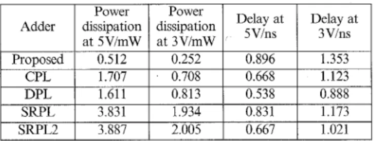
adder are summarised in Table 1. The proposed adder has a better power efficiency. It can also operate at a speed comparable to the other adders. In terms of area, the proposed adder is the most effective among all the studied adders. The transistor count of the proposed adder is 18 comparing to 48 for a DPL adder, 28 for a CPL adder and 28 for both the SRPL and SRPL2 adder. Besides, it does not require complementary input signals as in other adders. Thus, the overall circuit size is reduced farther.
Power Power
Adder dissipation dissipation at 5VlmW at 3VlmW Table 1: Comparison of adder performance
Delay at Delay at 3 Vlns 5vlns 0.252 0.896 1.353 1.707 0.708 0.668 1.123 1.611 0.813 0.538 0.888 SRPL 3.831 1.934 0.831 1.173 SRPL2 3.887 2.005 0.667 1.021
Conclusion: This Letter has described a low power and compact VLSI circuit for adder implementation. It is suitable for designs where power and size are the major design constraints. Compari- son showed that the proposed adder consumes less power than the other high speed CMOS based circuits including complementary pass transistor logic, dual pass transistor logic, and swing restored pass-transistor logic. The reduction in power consumption is the result of fewer number of transistors used in the design. Simula- tion results showed that the proposed adder consumes three times less energy than the CPL and DPL adder, and seven times less energy than the SRPL and SRPL2 adder, at both 3 and 5V sup- ply. Our simulation result also showed that the speed of the pro- posed adder is comparable to the others. Hence, the design of the circuit does not compromise the circuit performance with power consumption.
0 IEE 1997
Electronics Letters Online No: 19970464
A. Wu and C.K. Ng (EDA Centre, Department of Electronic Engineering, City University of Hong Kong, Tat Chee Avenue, Kowloon, Hong Kong)
3 February 1997
Reference
MATASUZAWA, A.: ‘Low-voltage and low-power circuit design for mixed analogueidigital systems in portable equipment’, IEEE J. Solid-State Circuits, 1994, 29, (4), pp. 470-480
KO, u., BALSARA, P.T., and LEE, w.: ‘Low-power design techniques for high-performance CMOS adders’, IEEE Trans. Very Large Scale Integr. Syst., 1995, 3, (21, pp. 321-333
YANO, K., YAMANAKA, T., NISHIDA, T., SAITO, M., SHIMOHIGASHI, K., and SHIMIZU, A.: ‘A 3.8-11s CMOS 16x16-M multiplier using complementary pass-transistor logic’, IEEE J. Solid-State Civcuits,
SUZUKI, M., SHINBO, K., YAMANAKA, T., SHIMIZU, A., SASAKI, K., and NAKAGOME, Y.: ‘A 1.5-ns 32b CMOS ALU in dual pass-transistor logic’, ZEEE J. Solid-State Circuits, 1993, 28, pp. 1145-I151
PARAMESWAR, A., HARA, H., and SAKURAI, T.: ‘A high-speed, low-
power, swing restored pass-transistor logic based multiply and accumulate circuit for multimedia applications’. Proc. IEEE 1994 CICC, pp. 278-281
NJOLSTAD, T., and AAS, E.J.: ‘Power consumption and performance of
low-voltage bit-serial adders’. Proc. IEEE 1996 ISCAS, pp. 4548
w u , A.: ‘High performance pipelined multiplier with fast carry-save adder’. 2nd NASA SERC Symp. VLSI Design, 1990
1990, 25, pp. 388-395
Optical switching in two-mode
semiconductor lasers via gain or loss
modulation
Ching-Fuh Lin, Pei-Cheng
Ku,
Yu-Li Hsueh and
Chaur-Shiuann Juang
Indexing terms: Semiconductor junction lasers, Optical switches The authors demonstrate an optical switching mechanism based on two-mode lasers in which bistability does not exist. Both theoretical analysis and experiment show that a small amount of gain or loss modulation is sufficient to cause switching between two oscillating modes.
Optical computing and optical communication require fast optical modulation and switching. Several methods have been used for this purpose. Direct intensity modulation on the laser diode pro- vides the advantage of simplicity, but it suffers the inherent limita- tion caused by relaxation oscillation. The use of a lithium niobate (LiNbO,) Mach-Zehnder modulator as an external modulator is an alternative candidate, but it usually requires a high drive volt- age ( V , 2 5) [1]. The use of an MQW electroabsorption modulator has recently attracted much attention [2]. However, it involves sophisticated material growth techniques. In this Letter, we pro- pose optical switching based on the two-mode laser via gain or loss modulation. The switching between the two oscillation modes could be achieved via a small amount of modulation. Similar switching used to be demonstrated in two-mode bistability [3], in which lasing is toggled between two competing cavity modes
[4
~ 61. However switching using bistability requires that the con-trolled variable is changed beyond the range for hysteresis. For the two-mode laser that does not have bistability, switching between the two oscillation modes can be even more easily acheved because no hysteresis regime needs to be passed during switching.
The idea of optical switching based on the two-mode laser is very simple and can be easily understood using two-mode compe- tition theory [7] although it can also be derived from the multi- mode rate equations. A slight extension from two-mode competition theory 171 can quickly lead to the condition for the simultaneously stable oscillation of both modes:
9 2
where S and C are cients, respectively; loss of each mode.
5 r -- Q2 - 12 Cl2
<-<--
g1 - 11 g2 - 12S
I
(1) 91 9 2 C2l s2the self-saturation and cross-saturation coeff-
g is the unsaturated gain and 1 is the cavity
I
a 0 0 0 2 O L 0 6 0 8 1 0 Loss of mode ICI/gl
0 0 0 2 O L 0 6 0 8 1 0
loss o f mode 1 (I/g)
a
bFig. 1 Illustrations of mode competition via loss modulation for g, = g, = 1, l2 = 0, and C,,/S, = C,JS, = 0.6 and 0.95 a 0.6 b 0.95 mode 1 mode 2 . . .
Switching between mode 1 and 2 should occur if gain or loss varies beyond the region given by eqn.
1.
The switching range also depends on the values of the ratios, S,lC2, and C121S2. Fig.1
shows the numerical calculation of the switching situation for differentratios
ofS1/C2,
and C,,IS,. Because this laser does not exhibit bistability, there is no hysteresis. For two-mode lasers with a very strong gain competition, the cross-saturation product C,,C,, is very close to the self-saturation product S,S,. Therefore, switching between these two modes can be achieved via only a very small amount of loss or gain modulation, as shown in Fig. lb.jmonochromotorl
PDI PD2
106812/ Fig. 2 Schematic diagram of optical switching in two-mode semiconduc- tor laser in experiment
PDI, PD2: photodetector G I , G2: grating
BS: beam splitter
Loss medium is cover glass mounted on rotary base
An experimental demonstration of optical switching between two oscillation wavelengths via loss modulation was carried out. A schematic diagram of the experimental setup is shown in Fig. 2. A standard ridge-waveguide laser diode is used in the setup. It has a 4 pn wide ridge-waveguide structure fabricated on an AlGaAsl GaAs substrate. The light emitted from the AR-coated facet
(R
= 4.6 x l k 3 ) is collimated byan
objective. A reflected-type grating telescope configuration [8] is used in the external cavity. As the mirror is placed at a focal distance from the lens, as shown in Fig. 2, different wavelengths will return into the same gain region, although they travel along different paths in the external cavity. V-shaped double slits are placed in front of the mirror to select two wavelengths for switching experiments.0 . 6
I
1
I
I 8 12 16
Loss of Long wavelength,%
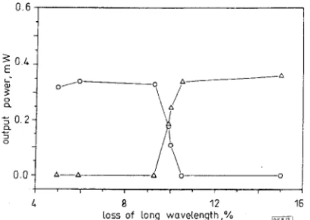
Fig. 3 Measured intensities of mode I (long Wavelength) and mode 2 (short wavelength) against insertion loss of mode I
0 long wavelength short wavelength
One or several cover glasses mounted on a rotary base are inserted in the path of mode 1, as shown in Fig. 2, so the loss of mode 1 can be modulated by rotating the cover glass or inserting more cover glasses. The Fabry-Perot effect of the cover glass makes the loss vary with rotating angle, but not monotonically
ELECTRONICS LETTERS
10th April 1997 Vol. 33
with the incident angle. Conversely, because the cover glass is very thin, it has little influence on the optical path and is experimen- tally found to cause a negligible wavelength shift
of
mode 1, regardless of the rotating angle in the experiment. Initially, theloss of
cover glass is adjustedto
havea
loss of 10% and the slitis
moved horizontally [8] to have two modes oscillating with almost equal intensity. Then switching between the two modes is observed as the cover glass is rotated. Fig.3
shows the intensity of each mode against calibrated loss. It is found that <1%
of loss varia- tion is sufficient to cause switching. Switching could also be possi- bly achieved by an electronically or optically controlled manner, e.g. via direct modulation on the monolithically integrated absorber or injection of the third-mode light, which will be further explored in the future.Such switching is different from the conventional wavelength tuning from one mode to another in a continuous way [9], where only one mode has a large gain and the others are suppressed with significant losses. In our work, both modes have significant gains and the switching is mainly caused by the cross-saturation effect. Therefore, the use of a single-stripe laser diode is essential because the two modes could then have a good overlap in the gain region to cause a strong gain competition. The farfield emission patterns for the oscillation of either mode (with one slit blocked) and the simultaneous oscillation of both modes were measured using a CCD camera. The nearly identical farfield emission patterns indi- cate that the two modes should overlap significantly in the gain region and so each mode has almost the same saturation effect on itself and the other. Therefore, S,lC,, and C121S, approach one and switching between these two modes can be achieved via a very small amount of loss. In addition, the cross-saturation characteris- tics of the two modes are mainly governed by the intraband relax- ation of the carriers. As a result, the switching speed is primarily limited by the intraband relaxation lifetime, instead of the sponta- neous-emission lifetime, and so is expected to be fast.
In conclusion, optical switching based on two-mode lasers is demonstrated theoretically and experimentally. Theoretical analy- sis shows that switching between the two oscillating modes can be achieved by a small amount of gain or loss modulation. The experiment demonstrates that < f l % of loss modulation is suffi- cient to cause optical switching between two lasing wavelengths in such a two-mode semiconductor laser. The efficient switching capability is due to the strong gain competition of the lasing modes.
Acknowledgment: This work is supported in part by the National Science Council, Taipei, Taiwan, Republic of China, under con- tract NSC85-2112-M-002-018. The authors would like to acknowl- edge Bor-Lin Lee for his technical assistance.
0 IEE 1997
Electronics Letters Online No: 19970435
Ching-Fuh Lin, Pei-Cheng Ku, Yu-Li Hsueh and Chaur-Shiuann Juang (Graduate Institute of Electro-Optical Engineering and Department of
Electrical Engineering, National Taiwan University, Taipei, Taiwan, Republic of China)
27 January 1997
References
1 LOI, K . K , SAKAMOTO, I , MEI, X.B., TU, C.W., and CHANG, W.S.C.: ‘High- efficiency I .3mm InAsP-GaInP MQW electroabsorption waveguide modulators for microwave fiber-optic links’, IEEE Photonics Technol. Lett, 1996, 8, pp. 626-628
2 SHEN, L., WIEDER, H.H., and CHANG, w.s.c.: ‘Electroabsorption
modulation at 1.3” on GaAs substrates using a step-graded low temperature grown InAlAs buffer’, IEEE Photonics Technol. Lett., 1996, 8, pp. 352-354
3 KAWAGUCHI, H.: ‘Bistability in laser diodes’ (Artech House, 1994) 4 KLEHR, A., MULLER, R , VOSS, M., and BARWOLFF, A.: ‘Gigahertz
switching behavior of polarization-bistable InGaAsP/InP lasers under high-frequency current modulation’, Appl. Phys. Lett., 1994,
64, pp. 830-832
TSUDA, H., and KUROKAWA, T.: ‘Side-light-injection MQW bistable laser using saturable absorption and gain quenching’, Electron. Lett., 1992, 28, pp. 1973-1975
5 UENOHARA, H., KAWAMURA, Y., IWAMURA, E., NONAKA, K.,
6 JOHNSON, J.E., and TANG, c.L.: 'Optical flip-flop based on two-mode
intensity bistability in a cross-coupled bistable laser diode', Appl. Phys. Lett., 1993, 63, pp. 3273-3275
7 SIEGMAN, A.E.: 'Lasers' (University Science Books, 1986)
8 LIN, : 'Selected multi-wavelength oscillation of a semiconductor laser in an external cavity'. Paper TuEB, 1995 Semiconductor Lasers: Advanced Devices and Applications, 1995, (Keystone, Colorado)
9 SCHREMER, A.T., and TANG, c.L.: 'External-cavity semiconductor laser with lOOOGHz continuous piezoelectric tuning range', ZEEE Photonics Technol. Lett., 1990, 2, pp. 3-5
...
Bandstop series stubs: To illustrate typical stub performance, the scattering parameters of a conventional, non-folded design are shown in Fig. 2. For this example the stub length is L = 1 9 0 0 ~ and the bandstop resonance occurs at 15GHz
cfo),
corresponding to a resonant length of -0.25 guide wavelengths. Each stub geom- etry considered herein exhibits a response which is similar to that of the non-folded stub up to the bandpass resonance at -2h; as an example, the scattering parameters of a 7 2 0 ~ long type DF-1 stub are also included in Fig. 2. In addition to resonant length, two other fignres of merit that will be used for comparison are the notch depth at& and the insertion loss at OS&, which are -16 and -0.9dB, respectively, for the non-folded design in Fig. 2.0
Bandstop series stubs
for
coplanar
waveguide on GaAs
T.M.
Weller,
K.J.
Herrick and L.P.B. Katehi
Indexing terms: Coplanar waveguides, Gallium arsenide
The authors present measured characteristics of several types of coplanar waveguide series tuning stubs printed on gallium arsenide. These stubs exhibit a bandstop response that is useful for microwave and m e t r e - w a v e filtering applications. Herein, the primary emphasis is placed on compact stub geometries which have resonant lengths as small as 0.1 guide wavelengths.
Introduction: Coplanar waveguide series tuning stubs are very use- ful and versatile components for microwave and millimetre-wave (mm-wave) applications [ 1 - 31. Typically, the series configuration
is implemented by routing the slots of the CPW line through the centre conductor, thereby deforming the centre conductor into multiple fingers. This laterally compact geometry enhances field confiiement and results in less radiation loss than that of stubs which are printed in the ground planes [4].
w2 T f design NF
, w
desiqn SF-I 6 * L design SF-2 design D F - 1 m-I 0 D 0 20 LO 1630121 frequency, GHzFig. 2 Measured scattering parameters for type NF-I ( L = 1900")
and type DF-I ( L = 7 2 0 ~ ) short-end stubs NF-1 Si,
NF-1 Sl, ...
- _ - _
DF-1 S,,-
__
-__
DF-1 S,,The electrical length of each short-end stub geometry at the first band-stop resonance is shown in Fig. 3. Here, the physical stub length is normalised to
5,
which is the free-space wavelength at&. The non-folded stubs resonate at -0.092&,, whde single-folded SF- 2 and double-folded DF-3 configurations resonate at 0.052% and 0.036&, respectively.0 1 0
. . . .
I " " I " " I
design DF-2 design DF-3
m
Fig. 1 Conventional and compact CPW series stub con$gurations In each case, S , refers to centre finger width and S, refers to width of all outer fingers
Coplanar ground planes are only shown for design NF
This Letter focuses on the use of short-end stub geometries in which the series stub is folded back upon itself to reduce size. The benchmark for the results is a configuration in which one pair of coupled slots is defined within the CPW centre conductor; this will be referred to as the conventional, or non-folded approach, and is shown in Fig. 1. More efficient use of circuit area can be achieved by using the single- and double-folded designs, which are also shown in Fig. 1. The primary objective of this work was to inves- tigate the relative merits of the folded stub designs on the basis of size, depth of the bandstop notch, and insertion loss.
The circuits were fabricated on 35Op-thick, high resistivity GaAs using the design specifications given in Table 1. In each case, the total ground plane width is 4(S
+
2W) and the gold lines were electroplated to a thickness of 2 . 7 ~ .0 x 1 \ O 0 . 0 6 . 0 2 0 2 0 f o , G H z LO 1630131 Pig. 3 Normalised short-end stub length against resonant frequency
&:
free-space wavelength at&-0- NF-1