國立交通大學
電信工程學系
碩士論文
新型三維微機電埋藏式結構與其應用
A Novel 3-D Embedded MEMS Structure And Its Application
研究生:林智鵬
指導教授:周復芳 博士
新型三維微機電埋藏式結構與其應用
A Newly 3-D Embedded MEMS Structure And Its Application
研究生:林智鵬 Student: Chih-peng Lin
指導教授:周復芳 博士 Advisor: Dr. Christina F. Jou
國 立 交 通 大 學
電 信 工 程 學 系 碩 士 班
碩 士 論 文
A Thesis
Submitted to Department of Communication Engineering College of Electronic engineering
National Chiao Tung University In Partial Fulfillment of the Requirements
For the degree of Master
In Communication Engineering June 2007
Hsinchu, Taiwan, Republic of China
II
新型三維微機電埋藏式結構與其應用
研究生 : 林智鵬 指導教授 : 周復芳 博士
國立交通大學電信工程學系碩士班
中文摘要
本論文裡提出了一種新型三維微機電埋藏式裝置與其相關的製作技
術,我們利用矽的深蝕刻技術與金屬化技術來製作一種新型的共平面波導
結構。
這種三維微機電埋藏式共平面波導,中心的傳導線的兩端經由微機電
技術被往下折並與地線重疊,這種結構可用來製作低特徵值阻抗的傳輸
線。跟傳統的共平面波導傳輸線比較,三維埋藏式共平面波導可以達到更
寬的特徵值阻抗(21–70 歐姆) 與較低的損耗;此外,三維埋藏式共平面波
導的製作並不複雜並可相容於
MMIC/VLSI電路的佈局與製程。三維埋藏式
共平面波導可達低特徵值阻抗的優點被利用於實現一個高效能、步階阻抗
式,操作在 X-頻帶的濾波器;此濾波器相較於傳統共平面波導所構成的濾
波器展現了明顯的優點,如較小的尺寸,較低的損耗,較寬的截止頻帶等
特徵。
A Newly 3-D Embedded MEMS Structure And Its Application
Student: Chih-peng Lin Advisor: Dr. Christina F. Jou
Institute of Communication Engineering
National Chiao Tung University
ABSTRACT
A novel embedded three dimensional (3-D) RF-MEMS devices and the related fabrication technology were shown in this thesis. The silicon deep etching and metallization technology were utilized to form a newly micromachined coplanar-waveguide (CPW) structure.
In these 3-D embedded CPW, the edges of the center conductors are bended down by micromachining techniques and partially overlapped with the ground plane to fabricate the low-impedance lines. Compared with the traditional coplanar-waveguide (CPW) lines, the 3-D embedded CPW lines show wider impedance range (21–70 Ω) and lower loss. Besides, the fabrication processes of the 3-D embedded CPW lines are not complex and compatible with MMIC/VLSI circuit layouts and processing. The advantages of 3-D embedded CPW for low-Zo lines are utilized to realize a high-performance stepped-impedance low-pass filter at X-band. The 3-D embedded CPW filter shows distinct advantages over the conventional CPW filter in terms of size, loss, skirt, and stop-band characteristics.
IV
Acknowledgement
在這兩年的碩士班生涯中,我首先要感謝指導教授周復芳老師,給
予我所研究的主題相當大的支持和體諒,讓學生在碩士生涯獲益良
多。並且特別感謝博士班黃俊源和陳一宇學長的耐心指點,在問題重
重的兩年提供我不少研究方向,並在學業上鼓勵及給予信心。
還要感謝 919 實驗室的每一份子,在這兩年間都能相處融洽並互
相砥礪互相切磋學問。多虧雄子豪和沈宜星無俚頭和低俗的搞笑,為實
驗室生活增添許多歡樂,宇清雖然鮮少出現在實驗室,不過他的精神
一直與我們大家同在,匯儀和俊緯學長也對我的碩士生涯帶來很大的
啟發和幫助,方瑞
嫻身為 919 唯一的女生,感謝她為這枯燥的環境帶
來一點活力,其他還要謝謝寶明和學弟們。
最後要感謝我的母親和妹妹,不管事精神上或是實質的供給,都讓
我無後顧之憂得順利取得碩士學位,也希望父親在天之靈能感到欣慰。
List of Figure
Fig.2-1. Schematic illustration of the basic process steps in
surface micromachining………..7
Fig.2-2.
Illustration
of
possible
bulk-micromachined
structure……….8
Fig.2-3. Typical sequence for the production of microstructure
based on the LIGA technique………...9
Fig.2-4. Phenomenon and the definition of step coverag………14
Fig.2-5. Poor step coverage shows in trench with high
aspect-ratio………15
Fig.2-6. Explanation of utilization of poor step coverage……..17
Fig.2-7. SEM picture of step coverage phenomenon………18
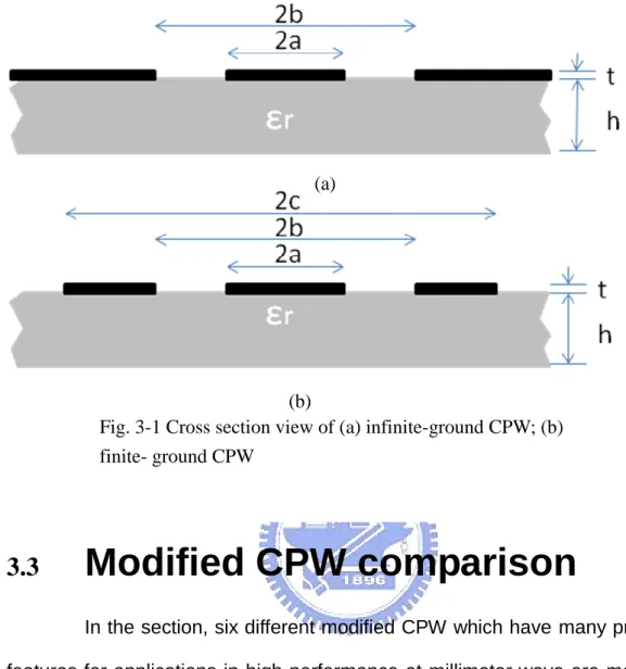
Fig.3-1.
Cross section view of (a) infinite-ground CPW; (b) finite-
ground CPW………..24
Fig.3-2.
Cross-sectional view of different CPW transmission lines
(a) elevated CPW; (b) insulated CPW; (c) micromachined
CPW with V-shaped groove; (d) microshielded
membrane CPW; (e) micromachined overlay CPW; (f)
3-D embedded CPW………27
Fig.3-3. Cross section view of CPW and 3-D ECPW………29
Fig.3-4. Comparison of characteristic impedance for 3-D
embedded CPW and traditional CPW with the same
surface area……….….30
Fig.3-5. Comparison of calculated loss for 3-D embedded CPW
and traditional CPW………30
Fig.3-6. Process flow the 3-D embedded CPW……….32
Fig.3-7. The equivalent circuit model for the contact pads and
impedance transformer………33
Fig.3-8. The comparison of the simulation and measurement
result……….35
Fig.3-9. Layouts and detailed dimensions for CPW and
OCPW………..37
Fig.3-10. Layout of CPW and 3-D embedded CPW on the
mask………....37
Fig.3-11. Simulation results of both CPW and 3-D embedded CPW
filter……….………..………...38
VI
Fig.4-2(a). Proposed antenna with 3-D embedded structure……..44
Fig.4-2(b). Antenna without 3-D embedded structure………44
Fig.4-3. The effect of varying the parameters (D) on the
impedance
matching………....……….45
Fig.5-1. DC block made by series CPW………48
Fig.5-2. coupling CPW DC block ………49
Fig.5-3. newly embedded DC block………49
CONTENTS
Chinese Abstract II
English Abstract III
Acknowledgement IV
List of Figures V
Contents VII
Chapter 1
INTRODUCTION ... 1
1.1 Background and Motivations ………1
1.2 Thesis Organization ... 2
Chapter 2
Micromachining and 3-D embedded MEMS structure ... 3
2.1 MEMS Technology ... 3
2.1.1 Surface Micromachining ... 4
2.1.2 Bulk Micromachining ... 5
2.1.3 LIGA ... 6
2.2 3-D Embedded MEMS technology ... 10
2.2.1 Introduction ... 10
2.2.2 Metal deposition ... 11
2.2.3 Utilization of poor step coverage ... 15
Chapter 3
3-D Embedded CPW ... 19
3.1 Introduction ... 19
3.2 Conventional CPW ... 20
3.3 Modified CPW comparison ... 24
3.4 Newly Structured CPW ... 28
3.4.1 Simulation of line characteristics ... 28
3.4.2 Fabrication ... 31
3.4.3 Measurement ... 33
3.4.3-1 Characteristic Impedance Measurement ... 33
3.4.3-2 Measurement Result ... 34
VIII
3.6 Conclusion ... 39
Chapter 4
Monopole antenna ... 40
4.1 Introduction ... 40
4.2 Antenna Design ... 41
4.3 Simulation Results ... 43
4.4 Conclusions ... 45
Chapter 1
INTRODUCTION
1.1
Background and Motivations
With the rapid growth of the microelectromechanical system (MEMS) in these years, it had been widely used in various fields, such as optical (MEMOS), Bio (BioMEMS) and RF (RFMEMS) applications. Besides, due to the increasing demands on the wireless systems, many researchers had paid a lot of attentions and efforts on the field of RFMEMS. The MEMS technology has the potential of replacing many Radio Frequency (RF) components such as switches, inductors, capacitors, phase shifters, surface acoustic wave (SAW) devices and ceramic filters used in today‟s mobile, communication and satellite systems. In many cases, such RF MEMS components would not only reduce substantially the size, weight, power consumption and component counts, but also promise superior performance in comparison with current technologies. In wireless and space applications complete RF systems, such as redundancy switch matrices, input multiplexers, and integrated front-end receivers, can be built with low cost, mass producibility and high reliability. Micromachining also enables new functionality and system capability that are not possible with current technologies. By using RF MEMS technology, System-on-chip (SoC) or System-in-package (SiP) wireless system can be possibly achieved. [1~3]
Due to the advantages of MEMS technology applied to RF components. This thesis uses a newly fabrication technology that is different from conventional Surface Micromachining technology. The new fabrication technology is to fabricate 3-D embedded RF-MEMS devices and it‟s slightly
2
similar to SCREAM process in Bulk Micromachining. The application of this technology is facilitate to form a newly structured CPW and a monopole patch antenna. The relative design and the characteristics are studied in detail in this dissertation.
1.2
Thesis Organization
In this thesis, MEMS technology had been employed to design and fabricate newly CPW structures and monopole antenna.
Chapter 2 is devoted to the general descriptions of the MEMS technology. The description only provides up to the level sufficient to comprehend the research work carried out in this thesis.
In chapter 3, a new 3-D embedded structure MEMS process is facilitate to form CPW and the 3-D embedded CPW line characteristics are studied in detail. To demonstrate the practical usefulness of the structure, and X-band Chebyshev seven-section step impedance low-pass filter has been designed and fabricated using low-Zo 3-D embedded CPW.
In chapter 4, the monopole patch antenna has been designed and fabricated with the 3-D embedded structure on the patch for ultra wide-band application.
In chapter 5, conclusions are made and the new ideas for further research are also suggested as the future works.
Chapter 2
Micromachining and 3-D
embedded MEMS structure
2.1 MEMS Technology
From a historical point of view, I would like to refer to a paper titled “There‟s plenty of room at the bottom” [4], which based on a seminar given in 1959 by the famous Nobel laureate physicist Richard Feynman. This paper is usually considered as the initial idea of the Microelectromachanical systems (MEMS) technology. In that paper, Dr. Feynman considered issues such as the manipulation of matter on an atomic scale and the feasibility of fabricating denser electronic circuits for computers. He also considered the issue of building smaller and smaller tools that could make even smaller tools so that eventually the individual atoms could be manipulated.
With the rapid growth and progress of the microelectronics technology which uses the single-crystal silicon as the basic material. The ability for realization of microstructure is well-established by using suitable integrated circuit (IC) process steps, such as thin film deposition, lithography, etching and so on. In the United States, such as a micro-fabrication technology is known as MEMS, whereas in Europe, it is called Microsystems technology (MST), and in Japan it is referred as Micromachines.
MEMS technology is a multi-disciplinary technology, it includes radio frequency(RF MEMS ), optical(Optical MEMS), chemistry, biology(BIO MEMS) [5] and other technologies. [6-7] Generally, it can be categorized into three
4
groups: surface micromachining, bulk micromachining, and LIGA (lithography, galvanoforming, moulding) [8-9]; each has their own advantages strengths weaknesses and applications [10]and will be discussed in the following subsections.
2.1.1 Surface Micromachining
Surface micromachining is a technology in which all functional features are built up on the surface of a substrate layer by layer[11,12]. This technique is based in deposition and patterning of thin film materials such as polysilicon, silicon nitride, or metallic thin film over a patterned sacrificial film such as silicon dioxide, polymer, or photoresist thin film. When the sacrificial layer is etched away, an undercut and freely suspended or movable structure can be obtained. The dimensions of these surface micromachined structures can be several orders of magnitude smaller than bulk-micromachined structures. The prime advantage of surface-micromachined structures is their easy integration with IC components, since the wafer is also used for IC elements fabrication. It should be noted that as miniaturization in immensely enabled by surface micromachining, the small mass structure involved may be insufficient for a number of mechanical sensing and actuation application.
Figure 2-1 shows the basic surface micromachining process. First a sacrificial layer is formed and patterned (Fig. 2-1a), followed by a similar process for the mechanical layer (Fig. 2-1b). Finally, the sacrificial layer is removed by sacrificial etching to leave the free standing structure (Fig. 2-1c). Note that the suitable sacrificial layer is dependent upon the mechanical layer used, with the important factor being the availability of an etchant which etches the sacrificial layer
without significantly etching the mechanical layer or the substrate. The prime advantage of surface-micromachined structures is their easy integration with IC components, because the wafer is also the working area for IC elements.
2.1.2 Bulk Micromachining
Bulk micromachining is the more mature one of the two silicon micromachining technologies. In bulk micromachining, structures are constructed by etching into a large single crystal substrate. Note that silicon is the most widely used material for substrate. The bulk micromachining technique can be divided into wet etching and dry etching of silicon according to the phase of etchants. Liquid etchants, almost exclusively relying on aqueous chemicals, are referred to as wet etching, while vapor and plasma etchants are referred to as dry etching. The term bulk micromachining comes from the fact that this type of micromachining is used to realize micromechanical structures within the bulk of a single-crystal silicon wafer by selectively removing („etching‟) wafer material. The microstructures fabricated using bulk micromachining may cover the thickness range from submicron to full wafer thickness (200 to 500 μm) and the lateral size range from submicron to the lateral dimensions of a full wafer. Bulk micromachining technique allows to selectively removing significant amounts of silicon from the substrate to form membranes on one side of a wafer. Fig. 2-2 shows some typical bulk- micromachining structures. Fig. 2-2(a) and (b) show the isotropic and anisotropic etching in silicon substrate. These properties are defined by the nature of the chemical reactions, the diffusion of reactants and products, the additives, and other factors. By removing parts of the substrate, floating structures can be formed, as shown in Fig. 2-2 (c). Note that the etching
6
stop layer is usually used in bulk micromachining technology to control the etching depth or construct the micro-structures, such as cantilevers and membranes.
By the combination of isotropic and anisotropic etching, robust structures can be built on or “in” the silicon wafers. Besides, by removing parts of the substrate, the performance of the RF device can be enhanced due to less substrate loss. Bulk micromachining technology now has attracted interest more in integration with complementary metal oxide semiconductor (CMOS) technology.
2.1.3 LIGA
LIGA is a German acronym standing for X-ray lithographie (X-ray lithography), galvanoformung (electroplating) and abformung (molding). The principal steps of the LIGA technology are shown in Fig.2-3. First, a thick photoresist is patterned with extend exposure to X-ray radiation, and the desired structures are formed after development (Fig.2-3a). Metal is then electroplated on the exposed conductive surface of the substrate, filling the space and covering the top surface of the resist. After the photoresist is removed, the metal structure is formed (Fig.2-3b). Then, the metal structure is used as a mold insert for injection molding to form plating bases (Fig.2-3c). The plating base replica is, in turn, used to electroplate additional metal parts, and is so-called second electroforming process (Fig.2-3d). After removing the plastic part, the final product is formed. The structures with high aspect ratio can be achieved by LIGA technique without the restriction of the crystal orientation. In addition, a large variety of materials are usable, like metals, ceramics, and polymers. The replication by micromolding offers the possibility of low cost mass production.
8
Figure 2-2: Illustration of possible bulk-micromachined structures. (a) Rounded, isotropically etched pits in a silicon substrate.
(b) Pyramidal pits etched into (100) and (110) silicon using anisotropic wet etchants, bounded by (111) crystal planes.
(c) A Pyramidal pits etched down to a buried etch-stop layer in (100) silicon, with an undercut cantilever beam
10
2.2 3-D Embedded MEMS technology
2.2.1 Introduction
VLSI and microwave monolithic integrated circuit (MMIC) applications require efficient use of chip real estate. Due to ever-increasing circuit densities, MMIC and VLSI designers seek to maximize the utility of the available space. This is demonstrated by the growing use of three-dimensional microstructures for CMOS trench isolation [13], V-grooved silicon solar cells [14], VMOS FET channel regions [15] and optical waveguides [16].
The trench waveguide structure was first described in1988 [17]. Trench waveguide is a three-dimensional interconnect structure, utilizing not only the surface area of the substrate but also the unused bulk of the substrate. However, the related research about the trench waveguide structure is rarely found. In this thesis, the fabrication steps of the trench waveguide are varied and simplified. The fabrication steps of the 3-D embedded CPW lines are shown in the following sections, and its characteristics are also studied in detail.
The advantages of trench waveguide as a circuit interconnect include the following features:
(i) Compatibility with MMIC/VLSI circuit layouts and processing (ii) Ability to realize low characteristic impedances
(iii) Reducing current density near conductor strip edges, thus reducing conductor loss
(iv) Allowing the use of thick substrates during processing, thus reducing the damage during handling and enhancing the yield of production.
(vi) Exempting from crosstalk due to the presence of ground plane between any adjacent lines.
2.2.2 Metal deposition
Chemical Vapor deposition (CVD) and Physical Vapor Deposition (PVD) are two kinds of metallization technologies used in IC fabrication processes. They are different in reaction mechanism and deposition characteristics. Both of them will be described concisely as follows.
Chemical Vapor Deposition (CVD) is the process of depositing a solid film on the wafer surface through a chemical reaction of a gas mixture. The wafer surface or its vicinity is heated in order to provide additional energy to the system to drive the reactions. There are several essential aspects of CVD listed in below.
1. Chemical action is involved, either through chemical reaction or by thermal decomposition
2. All material for the thin film is supplied by an external source. 3. The reactants in a CVD process must start out in the vapor phase.
The fundamental CVD reactions have following steps and the explanations of the reaction mechanism are also shown in it.
1. Transport of the reactants by forced convection to deposition region. 2. Gas-phase reactions leading to the formation of the film precursors and
by-products.
3. Mass transport of the precursors to the growth surface of the wafer. 4. Adsorption of the precursors to the wafer surface.
12
6. Surface process, including chemical decomposition or reaction, surface migration to attachment sites, site incorporation, and other surface reaction. 7. Desorption of the by-products of the surface reactions.
8. Transport of byproducts by diffusion through the boundary layer and back to main gas stream.
9. Transport of byproducts by forced convection away from the deposition region.
CVD is widely used to deposit metal layers. Metal CVD is a conformal deposition and has well gap-filling ability. It is usually used to fill the contact via thus formed the plug between adjacent metal layers. However, due to its conformal deposition and well gap-filling capability, metal CVD is not suitable for our applications in fabricating 3-D CPW structures..
Physical Vapor Deposition (PVD) is the process of depositing thin
films by means of heating or sputtering the solid target into vapor phase and then condenses on the surface of the substrate. The condensing of the vapor thus can form a thin film on the wafer surface. There are several differences between PVD and CVD. PVD techniques are generally more versatile than CVD methods, allowing for the deposition of almost any material. The constituent species, individual atoms or molecules, are produced by either evaporation of a solid or the atoms from a source “target”. These atoms or molecules then travel though a vacuum or a very low pressure gas phase, impinge on the wafers, and condense on the surface to form the film. CVD has better step coverage of deposited thin film and PVD has better film quality. There are two methods of PVD metal deposition, Evaporation and Sputtering. In IC metallization process, sputtering is the most common PVD process. Because sputtering process can deposit high quality metal layers also the uniformity and reliability are very good.
Besides, sputtering has better step coverage than evaporation. Though that the sputtering can not achieve conformal deposition as metal CVD do. It becomes a benefit to our applications surprisingly. DC sputtering thus is chosen as the best candidate to do the metallization process in this thesis due to its limited step coverage.
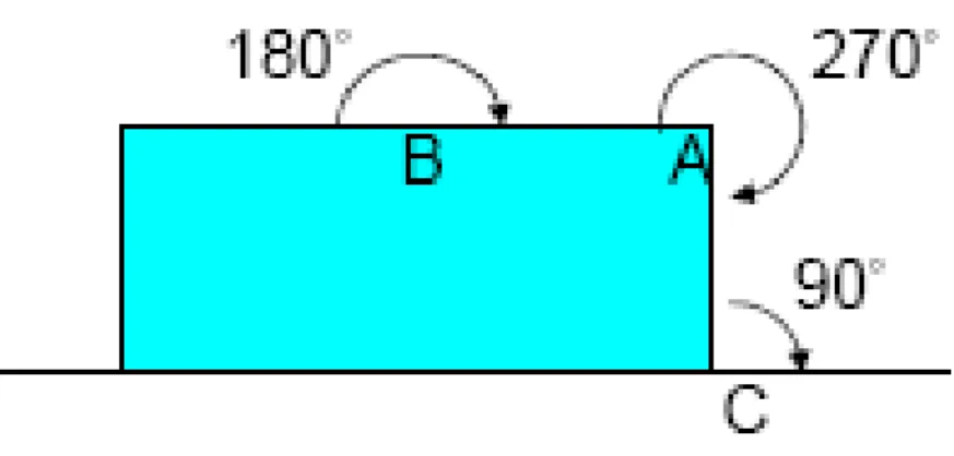
Step coverage is a measurement of the deposited film reproducing the
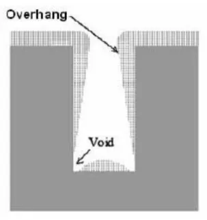
slope of a step on the substrate surface. It‟s a very important parameter of the PVD process. Fig. 2-4 shows the definition of aspect ratio, side-wall step coverage, bottom step coverage, conformality and overhang. Step coverage depends on the arriving angle and the surface mobility of the precursor. The arriving angle mentioned above is shown in Fig. 2-5. As we can see that angle A has the largest arriving angle, 270°, and the angle C is the smallest. When the source material diffuses through the boundary layer, more source material will arrive to angle A than angle C. If source material react immediately after absorb to the wafer surface and without movement, angle A will have more deposition than angle C and overhang will be formed as shown in Fig.2-6. Overhang is not expected. Because overhang on each side of the trench top will soon merges and causes a void (keyhole). By reducing the process pressure, MFP of precursor will increase. When MFP is longer than the gap depth, there will be few collisions inside the gap.Therefore precursors have little chance to go backward to reach corner A from inside the gap. This will efficiently reduce the arriving angle and improve the step coverage.
As mentioned in above paragraph, poor step coverage is unexpected in VLSI process. Because it will cause voids in metal layer then increase the metal resistivity and cause defects and reliability problems. Thus, evidently evaporation is not suitable for our application. In this thesis we will take the
14
advantage of limited step coverage of metal deposition of sputtering. The desired 3-D embedded structure is mainly relying on the utilization of this limited step coverage and the details will be shown in the following subsection.
Fig 2-4. The phenomenon and the definition of step coverage
2.2.3 Utilization of limited step coverage
As mentioned in last paragraph, we expect conformal deposition than limited step coverage deposition in semiconductor fabrication. But the characteristic of limited step coverage deposition can be utilized to form the 3-D embedded RF-MEMS devices that will be demonstrated latter in this thesis. As shown in Fig. 2-7, when the trench is deep enough, the aspect ratio of the trench will be larger than the ability of sputtering. Thus, a discontinuity will start to appear at the bottom of the side wall of the trench after thin film deposition. It means that terminal A and B in Fig. 2-7 are disconnected and there is a big
Fig 2-6. Overhang and void formed during thin film deposition. trench
16
parallel plate capacitor in the trench. Hence, it can be utilized to form a strong coupling, or tight coupling structure.
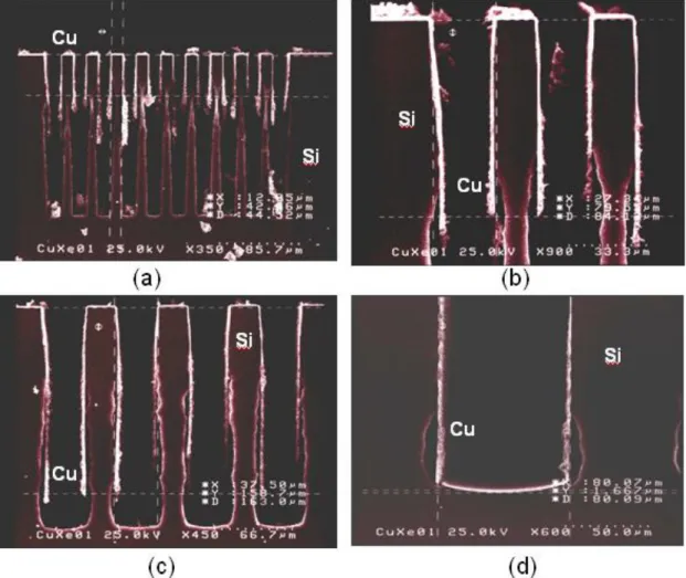
Fig. 2-8 (a) ~ (d) are the SEM pictures of Cu film deposition with DC sputtering onto the trenches with different aspect ratio followed with XeF2 isotropic etching. Note that the XeF2 isotropic etching can make us observe the depth of the deposited Cu film in the trench more easily. Besides, we can use such isotropic etching to remove the silicon underneath the CPW lines for improving its performance in the future. In Fig. 2-8, we can find that the aspect ratio of the trench must be larger than 4 so that the discontinuity could happen. It is worthy to note that this result is just suitable for certain process condition, if we modify the conditions of thin film deposition, such as pressure, gas flow and so on, the minimum aspect ratio of the trench would be different. Thus the different size of parallel plate capacitor can be achieved.
A lot of RF passive devices can be constructed by using the high coupling structure. For example, low impedance transmission line, DC block, filter, lateral type switch/relay, phase shifter …etc. Hence, we believe that we can have smaller RF passive devices with better performance by using such 3-D structure.
Fig. 2-7 Explanation of the utilization of limited step coverage
18
Fig. 2-8 (a) ~ (d) are the SEM pictures of Cu film deposition with DC sputtering onto the trenches with different aspect ratio followed with XeF2 isotropic etching.
Chapter 3
3-D Embedded CPW
3.1
Introduction
Conventional coplanar-waveguide (CPW) has been widely used in microwave and RF system. But it suffers from high conductor losses at high and low characteristic impedance extremes due to its narrowing of the center conductor and slot width, respectively [13], [14]. Moreover, very low-Zo lines are practically impossible to realize in CPW due to the minimum slot size limit imposed by the fabrication process. Therefore, designers are often restricted in their choice of impedance values when designing monolithic-microwave integrated-circuit (MMIC) circuits with CPW.
There were several papers trying to reduce the losses of the high-Zo lines, by different ways [15]–[17]. As far as the low-Zo lines are concerned, a way to elevate the edges of the center conductors and partially overlapped with the ground plane had created and showed great line characteristics. The overlap between signal and ground lines makes very low-Zo lines possible without the slot size constraint. However, the fabrication process is complex and it can‟t be facilitate to SoC system.
In this thesis, a new 3-D embedded CPW structure, in which the edges of center conductor are partially bended and overlapped with ground, as shown in Fig. 3-2(f). The broad ranges of characteristic impedance and low losses can be achieved by using such 3-D structure. The structure used in this thesis is sample comparing to other relative low-Zo CPW lines structures. Only 2 masks are needed.
20
The loss characteristics of the 3-D embedded CPW lines are studied in detail for various dimension values. Field simulations and comparative experiments have been performed to fully characterize the 3-D embedded CPW lines. An X-band Chebyshev seven-section stepped-impedance low-pass filter (LPF) is simulated and fabricated by using the low-Zo 3-D embedded CPW lines. To demonstrate the practical usefulness of the 3-D embedded CPW, an X-band 0.5-dB equiripple Chebyshev seven-section stepped-impedance low-pass filter (LPF) has been designed and fabricated using low-Zo 3-D embedded CPW lines. It is shown that low-Zo 3-D embedded CPW lines can be used as lumped capacitors, which help to solve the inherent problems of the LPF using distributed structures, such as low cutoff rates and poor attenuation in the stopband. Compared with the CPW filter, the 3-D embedded CPW filter shows distinct advantages such as small size, low insertion loss, sharp skirt characteristics, and wide stopband.
3.2
Conventional CPW
The coplanar waveguide (CPW) was invented by Wen [18] in 1969 as a novel surface strip transmission line fabricated on a dielectric substrate. The CPW transmission line has demonstrated several advantageous features over the conventional microstrip line, for instance, easy surface mounting of external devices, easy fabrication of both shunt and series passive elements, low-frequency dispersion, and easy adjustment of desirable characteristic impedance. Since its proposal, the CPW technology has been progressively gaining a tremendous application in exploration of advanced RF and microwave integrated circuits, modules, and subsystems. For this purpose, much effort has
been carried out to construct a new variety of modified CPW transmission lines with varied cross-sectional configurations and accurately characterize their propagation performance in theory and experiment, as summarized in two relevant books [19,20]. In particular, various static and fullwave methods have been effectively developed to deal with these inhomogeneous transmission lines and derive the two per unit length transmission parameters, i.e., effective dielectric constant and characteristic impedance.
GEOMETRY AND ANALYSIS
The conventional CPW transmission line [18] consists of the central strip conductor and the two infinite-width ground planes on two sides that are formed in close proximity on the same surface of a dielectric substrate with finite height. By equalizing the electric potentials at the two ground planes, only the even symmetric dominant CPW mode can be excited. At high frequencies, this CPW mode becomes non-TEM with a longitudinal component of magnetic field. In such a case, the tangential magnetic field, on the surface of the coupled slots between the strip conductor and two ground planes, becomes elliptically polarized.
In Wen‟s work [18], the relative permittivity is assumed much larger than the unity ( 1) so that the finite height of a substrate can be reasonably treated as the infinity ( ) for simplifying the theoretical analysis. But, in practice, and h have to be finite as shown in Fig. 3a. Also, the actual ground width of this CPW is usually finitely wide so as to formulate the call finite-ground CPW or FGCPW as shown in Fig. 3b.
22
a variety of CPW transmission lines in terms of per unit length characteristic impedance and propagation constants by developing the quasistatic and full-wave analysis approaches [19,20]. The quasistatic conformal mapping technique was initially utilized to model the CPW line with infinite dielectric thickness. However, an accuracy of larger than 1% for a wide range of physical dimensions and dielectric permittivity is achieved as compared with that of the full-wave spectral-domain method [21]. Of vital importance, this technique gives rise to analytical expressions for effective dielectric constants and characteristic impedance in terms of the ratio of complete elliptic integral of the first kind and its complement, K(k)/K‟ (k), where k is the variable.
The detailed mathematics of this procedure can be found in the literature [e.g., 1–7] and are not discussed here. In this section, the infinite-ground CPW is characterized by the three sets of closed-form design formulas in Figs. 3-1a with respect to various physical dimensions. The analytical expressions of the ratio K(k)/K‟ (k), are provided below in two different regions of the variable k for infinite- and finite-width-ground CPWs:
For conventional CPW with infinite-width ground as in Fig. 3-1a, the two variables and are defined in terms of the dimensions a, b, and h,
As such, the per unit length effective dielectric constant and characteristic impedance can be deduced:
By verifying the results of Eqs. (3) and (4). The impedance (Zo) definitely increases as the slot is widened for all the four listed h/W because of reduced capacitive coupling between the strip conductor and two ground planes. As h/W increases, the Zo curve converges to that with very thick thickness (h/W=20). Meanwhile, the effective dielectric constant ( ) falls down as the slot width is enlarged under the fixed finite thickness (h/W) and it eventually becomes almost independent of h if h/W is larger than 20. It can be further deduced from these results that the effect of finite dielectric substrate is almost ignorable if h exceeds 2b=W+2S.
24
3.3
Modified CPW comparison
In the section, six different modified CPW which have many promising features for applications in high-performance at millimeter-wave are mentioned and described briefly. The theoretical characteristics of multilayered CPW transmission lines have been reported in the literature [5–7]. In this paragraph, two of these CPW structures that exhibit enhanced electrical performance such as elevated and insulated CPW, are discussed here (check cross-sectional views in Fig. 3-1(a) (b)). The elevated CPW in Fig. 3-2a is proposed [22] for construction of a nonlinear transmission line fabricated with Schottky diodes on GaAs substrate. This CPW has several attractive features such as low loss, high wave velocity, and broad frequency bandwidth. By using the full-wave approach, its propagation performance is characterized with respect to varied elevated
Fig. 3-1 Cross section view of (a) infinite-ground CPW; (b) finite- ground CPW
(a)
heights [23]. The CPW is fabricated on silicon substrate for low-cost application in radio frequency integrated circuits (RFICs). Due to high attenuation, the CPW is usually constructed by forming an insulated layer, such as low-loss polyimide [24] or SiO2 [25], above the silicon substrate, as shown in Fig. 3-2b. The measured results show that attenuation can be reduced if the insulated layer is thick relative to the strip and slot widths [24].
The silicon micromachining technique has been developed to effectively remove the lossy substrate or dielectric material below, above, or around the coupled apertures in CPW in an effort to minimize propagation loss and reduce frequency dispersion. Fig. 3-2c shows the micromachined CPW [26], where the material underneath the coupled apertures is partially removed for construction of the free-space V-shaped grooves. This resulting line minimizes the total propagation loss since the EM fields are distributed mainly in the lossless V-shaped region and current density flow on the conductor is reduced. Fig. 3-2d shows a practical microshielded membrane CPW that is fabricated by attaching two silicon wafers together [3, 26]. The upper wafer, with a metallized cavity, supports a membrane with the CPW. Because of an extremely thin electric membrane, the overlapping capacitances between the top ground planes and cavity sidewalls are very large in the microwave region, thus virtually short-circuiting the overlapped region. The lower wafer is metallized on the top surface and provides the bottom wall of the cavity. Fig. 3-2e shows a micromachined overlay CPW [27]. By partially elevating the edges of the central conductor and further overlaying them with the two outer ground planes, this CPW has a lower propagation loss because the current density is redistributed on the conductors and the impedance range widens. At last, Fig. 3-2f shows the three-dimensional CPW [28]. By etching the trench and angle evaporation, the
26
structure can be fabricated. The overlay zone between central conductor and ground planes are within the trench. The loss reduction concept is similar to the structure in Fig. 3-1e. But, by doing so, the specified orientation of wafer is needed and two angle evaporation processes enlarge the complexity of the transmission line fabrication. Such a process can not be applied and integrated with other devices for further applications.
In this thesis, the focus is on the design and fabrication of 3-D embedded structure. The complete analysis of the structure is shown in the following section.
Fig. 3-2 Cross-sectional view of different CPW transmission lines (a) elevated CPW; (b) insulated CPW; (c) micromachined CPW with
V-shaped groove; (d) microshielded membrane CPW; (e) micromachined overlay CPW; (f) 3-D embedded CPW
28
3.4
Newly Structured CPW
3.4.1
Simulation Results
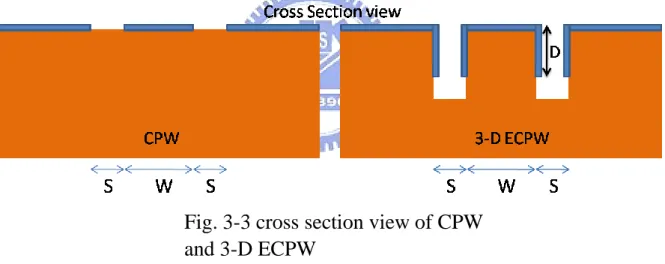
The schematic of a 3-D embedded CPW is shown in Fig. 3-3 together with the associated parameters. The edges of the center conductor and ground plane are partially bended using micromachining techniques and two of them are overlapped with each other. It can be easily varied the characteristic impedance from high-Zo to low-Zo by increasing the overlap (“D” in Fig. 3-3) between the center conductor and the ground. The 3-D embedded CPW helps to reduce the conductor loss by reducing the field concentration and current crowding at the edges of the signal lines. Moreover, the 3-D embedded CPW is expected to reduce not only the conductor loss, but also the substrate loss by confining the electric field in the air between the overlapped conductor plates.
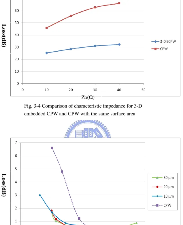
The loss analysis of both the 3-D embedded CPW ( W=10, 20 and 30μm ; D= 5, 10, 20, 40, and 80μm) and CPW ( and W=40, 30, 20, 5 and 2μm) lines is performed using a 525-μm-thick silicon substrate ( =11.9 ) and the metal plane thickness is set to be 1μm. In the 3-D embedded CPW, the width of the center conductor touching the substrate is fixed at 27μm (S=27μm). All simulations have been carried out at 20 GHz with a commercial electromagnetic (EM) simulator (Ansoft HFSS). The simulation results are shown in Fig. 3-4 and Fig. 3-5. From Fig. 3-4, as CPW and 3-D ECPW consume the same surface area, 3-D ECPW can reach lower characteristic impedance. In case of the CPW lines, it is practically impossible to achieve the values of characteristic impedance lower than 30 Ω. Due to the limit of photolithography, the minimum spacing between the signal and ground lines is about 2 μm. On the contrary, a
wide impedance range down to 20 Ω can easily be obtained by controlling the overlap (D) in the 3-D embedded CPW.
The loss of 3-D embedded CPW lines with a trench width 20μm is maintained to less than 2 dB over a wide impedance range from 20 to 70 Ω, while that of the CPW line increases rapidly as the impedance decreases below 30–40 Ω.
Fig. 3-3 cross section view of CPW
and 3-D ECPW
30
Fig. 3-5 Comparison of calculated loss for 3-D embedded CPW and CPW
Fig. 3-4 Comparison of characteristic impedance for 3-D embedded CPW and CPW with the same surface area
Zo(Ω) Zo(Ω)
Lo
ss
(dB
)
Lo
ss
(dB
)
3.4.2
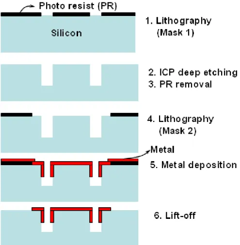
Fabrication Process
The 3-D embedded CPW lines in this thesis are fabricated on both the silicon substrates and the high resistivity silicon substrates. The fabrication steps are identical on two different substrates. The steps of fabrication process are shown in Fig. 3-6. First of all, a 5000 Å silicon dioxide is grown on the silicon substrate surface for better isolation and it can slightly reduce the conduction loss and substrate loss. In the first step, the desired trench position and size are defined by standard photolithography process. In the next step, trenches are fabricated by deep etching technology with Inductively Coupled Plasma (ICP) system. The ICP etching system has widely been used in silicon-based IC process for deep trench formation. In the forth step, the dry film photoresist is used in the photolithography process to define the desired position and area for the metallization step as followed. It is worthy to note that dry film photoresist used here is necessary for preventing the photoresist flowing into the trench. Then the metal sputtering process is used for the deposition of copper (Cu) film. Note that the thickness of the Cu is about 1 μm and a titanium (Ti) with 100 nm thick is used as the adhesion layer. The reasons for the use of sputtering process are mentioned in the section 2.2.3. In the last step, we want to get rid of the metal in the unwanted place. The “lift-off” technology is utilized to remove the photoresist together with the metal above it. Finally, the 3-D structure is completed, as shown in Fig. 3-6.
32
3.4.3
Measurement
3.4.3-1 Characteristic Impedance Measurement
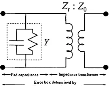
It‟s the important issue to determine the characteristic impedance of transmission lines on the lossy substrates such as silicon. This issue has been studied by several researchers. In this thesis, we adopt the method that was published in Dylan F. Williams‟ paper [29].
Fig. 3-7 shows a simple model for a transition between a probe tip and a transmission-line. The model consists of a lossy shunt contact-pad with admittance Y followed by an impedance transformer mapping the reference impedance Zr, of the probe-tip calibration into the reference impedance Zo of the second-tier TRL calibration. The transmission matrix X of the circuit in Fig. 3-7 is
Where
Fig. 3-7 The equivalent circuit model for the contact pads and impedance transformer
34
When transition parasitics are dominated by contact pad capacitance and conductance, the error box X’ measured by the calibration comparison method will be approximately equal to X.
From reference [30] estimates Г as:
It shows that Гo is insensitive to arbitrarily large reference plane transformations of the probe-tip calibration. However, while Гo, may not be sensitive to these reference plane transformations, (1) shows that it will be sensitive to Y.
On the other hand, the term YZr/2 in (1) adds to X21 but subtracts from X12,
so its effect cancels completely from the mean . Thus, even for
very large Y,.
. In the new method we propose here, we will use
(2) and the estimate
which is insensitive to contact-pad capacitance and conductance Y, to determine
Zo.
3.4.3-2 Measurement Results
The S-parameters of the lines were measured by HP 8510C network (2)
(4) (3)
analyzer, and the method for characteristic impedance calculation is as described in section 3.4.3-1. The 3-D embedded CPW structure of trench
width=10 um. The conventional CPW of W= 20μm and 30μm are also measured. The measurement result comparing to the simulation result shows in Fig. 3-8. In the figure, we can find that the measurement results are quiet reasonable
comparing to the simulation data.
Fig. 3-8 The comparison of the simulation and measurement result. Zo(Ω)
Lo
ss
(dB
36
3.5 Low-pass Filter Application
In this thesis, we have employed low-Zo 3-D embedded CPW lines as capacitive elements in the stepped-impedance LPF. Thus, this LPF is expected to benefit from the low-loss and low-Zo capabilities of 3-D embedded CPW structures. For experimental verification, X-band Chebyshev seven-section stepped-impedance LPFs have been implemented using both CPW and 3-D embedded CPW lines on 525- μm-thick silicon substrate. The element values of the filters were calculated using a standard design procedure [11]. The simulation is carried out by Ansoft HFSS. Based on these informations, the lengths of each section were determined so that they might meet the element values of the filters. In the actual layout, the inductive sections were realized using meandered high-Zo CPW lines for size reduction and were common to both filters. The capacitive sections were implemented with low-Zo 3-D embedded CPW lines for the 3-D embedded CPW filter, while low-Zo CPW lines were employed for the conventional CPW filter. The detailed dimensions and the schematics are shown in Fig. 3-9 and Fig. 3-10 shows the mask layout of the filters. The length of the center conductor of low-Zo lines was fixed at 97 μm for both filter cases. Due to the enhanced capacitance, the 3-D embedded CPW line showed lower characteristic impedance and smaller effective dielectric than the CPW line. Therefore, the length of low-Zo lines of the 3-D embedded CPW filter was effectively reduced. In this way, the capacitive sections using the low- 3-D embedded CPW line show the properties more similar to the lumped elements. The comparison between the simulated performance of both filters is shown in Fig. 3-11. Besides the benefit of size reduction as I stated earlier, the 3-D embedded CPW filter offers additional advantages of low insertion loss, and
sharp skirt characteristic.
Fig. 3-9 The layouts and detailed dimensions of CPW and OCPW X-band LPFs.
38
Fig. 3-11 Simulation results of both CPW and 3-D embedded CPW filters. X-band LPFs. 0 5 10 15 20 25 30 35 40 -60 -50 -40 -30 -20 -10 0 S11 3-D embedded S21 3-D embedded S21 traditional S11 traditional Frequency(GHz) 0 2 4 6 8 10 12 -2 -1.8 -1.6 -1.4 -1.2 -1 -0.8 -0.6 -0.4 -0.2 0 S21 S21 3-D embedded S21 traditional Frequency(GHz) L oss(d B )
3.6 Conclusions
In this section, a 3-D embedded CPW structure was developed to solve the loss problems of the low-impedance CPW lines and to extend the usable impedance ranges. Micromachined technology was employed to bended both the center conductor and ground plane partially overlap with each other. A systematic and comparative study has been performed to characterize the 3-D embedded CPW lines. Compared with the conventional CPW, the fabricated 3-D embedded CPW lines with 20- μm trench width showed lower losses (less than 3 dB on silicon substrate at 20 GHz) over a wider range (20–90Ω). To demonstrate practical usefulness of the 3-D embedded CPW lines, an X-band stepped-impedance LPF was fabricated using 3-D embedded CPW lines. The 3-D embedded CPW LPF showed distinct advantages over the conventional CPW filter such as lower loss and reduced size, together with improved spurious responses, including sharp skirt and wide stop-band characteristics. Thanks to their wide impedance and low-loss characteristics, the proposed 3-D embedded CPW is expected to be very useful for integration with various uniplanar microwave/millimeter-wave integrated circuits.
40
Chapter 4 Applications in Monopole Antenna
4.1 Introduction
Nowadays, wireless communication systems are becoming increasingly popular. However, the technologies for wireless communication still need to be improved further to satisfy the higher resolution and data rate requirements. That is why ultra wideband (UWB) communication systems covering from 3.1 GHz to 10.6 GHz released by the FCC in 2002 [31] are currently under development. Various antennas for wideband operation have been studied for communications and radar systems for many years [32], [33]. The design of wideband antenna is a very difficult task especially for hand-held terminal since the compromise between size, cost, and simplicity needs to be achieved. In UWB communication systems, one of key issues is the design of a compact antenna while providing wideband characteristic over the whole operating band. Due to their appealing features of wide bandwidth, simple structure, omidirectional radiation pattern, and ease of construction several wideband monopole configurations, such as circular, square, elliptical, pentagonal, and hexagonal have been proposed for UWB applications [34]–[36].
In this thesis, a new microstrip-fed patch antenna with a tuning 3-D trench is presented. In order to improve the impedance bandwidth, a 3-D trench on the patch and stepped ground are used in the design of the antenna.
4.2 Antenna Design
Fig. 4-1 (a) shows the evolution of the proposed antenna fabricated on the quartz substrate, which consists of a rectangular patch with two notches at the two lower corners of the rectangular patch and a truncated ground plane with the notch structure. These notches alter the electromagnetic coupling between the rectangular patch and the ground plane. Matching improvement can also be obtained by inserting a slot in the truncated ground plane. It is found that much enhanced impedance bandwidth can be achieved for the proposed antenna. Moreover, the 3-D embedded technology mentioned in chapter 2 will be applied to this monopole antenna in order to improve the band-width and matching. The proposed antenna has compact dimension of 36 mm X 16 mm with thickness of 0.52 mm and relative dielectric constant of 3.7. From the simulation, the optimized dimensions are: W=8.4 mm, L=10.6 mm, Wg=16mm, Lg=23.5 mm, Ws=6 mm, Ls= 1mm, Wn=1.6 mm, Ln=1.4 mm, We=2.4mm, Lf1=1mm, Lf2=23mm and the width of fed-in line is 1mm. The detail trench dimensions is shown in Fig. 4-1(b)
42 Lf1 Lf2 (a) (b) D
4.3 Simulation Results
Fig. 4-2 (a) and (b) show the comparison of the simulation results of the antennas with and without 3-D embedded structure. The bandwith for -10 dB return loss covers the range of 3.28~11.2 GHz. Comparing with the antenna without 3-D embedded structure, the proposed antenna shows better impedance matching.
The geometrical parameters related to the trench include the dimensions of the trench (0.05mm X 0.01mm) and the metal depth (D). Fig. 4-3 exhibits the effects of varying the parameters on the impedance matching. From Fig. 4-3, we can see that the length of the metal (D) would affect the impedance matching especially at the lower operating frequencies around 5 GHz and increasing the length extend the higher edge frequency of the bandwidth. The depth of the metal (D) and location of the trench slightly affect the higher edge frequency. In general, all the trench-related parameters influence the impedance matching to a certain extent.
44
(a)
Fig. 4-2 (a) proposed antenna with 3-D embedded structure; (b) the antenna without 3-D embedded structure
4.4 Conclusions
In this section, a monopole patch antenna has been proposed for promising ultrawideband applications. The antenna has been designed to supply a new matching structure by placing the trench on the radiator. The study has shown that the trench is able to vary the matching of bandwidth of the antenna and offer a better matching characteristic.
Fig. 4-3 The effect of varying the parameters (D) on the impedance matching.
46
Chapter 5 Conclusions and Future Works
5.1
Conclusions
The 3-D embedded structure mentioned in this thesis shows several advantages as below:
(i) compatibility with MMIC/VLSI circuit layouts and processing, (ii) ability to realize low characteristic impedances,
(iii) reducing current density near conductor strip edges, thus reducing conductor loss,
(iv) allowing the use of thick substrates during processing, reducing damage during handling and enhancing yield,
(v) eliminating the need for via holes, thus reducing associated parasitics,
(vi) exempting from crosstalk due to presence of ground plane between any adjacent lines.
The 3-D embedded structure is used to design the newly structured CPW and monopole antenna. Compared with the conventional CPW, the fabricated 3-D embedded CPW lines with 20- μm trench width showed lower losses (less than 3 dB on silicon substrate at 20 GHz) over a wider range (20–90Ω). Moreover, the 3-D embedded CPW LPF showed distinct advantages over the conventional CPW filter.
The monopole antenna has been designed to supply a new matching method by etching the trench on the radiator. The designed antenna satisfies the 10 dB return loss requirement from 3.2 to 11 GHz and provides good monopole-like radiation patterns.
5.2 Future Works
The results presented in this thesis represent a work in progress, and hence there are still other efforts can be done. The 3-D embedded CPW mentioned in chapter 3 is considerable to integrate to MMIC/VLSI process. Besides, other applications of 3-D embedded structures are described as follows:
(1) DC Block
DC Block is widely used in microwave circuit in order to isolate the DC voltage level from different blocks. In general, DC block must have very low insertion loss and tolerable to high voltage. In normal high frequency circuit, DC block is composed of electromagnetic coupling structure. Fig. 5-1 and Fig. 5-2 show the layouts of traditional DC blocks.
However the structures in Fig. 5-1 and 5-2 are a 2-D circuit, they consume big area of the substrate to get the desired capacitance value. Moreover, it can only operate in high frequency because the capacitance value is not big enough. By using the 3-D embedded structure, high coupling effect can be achieved due to the increase of the effective capacitance and the area consumption will be less. Both top and cross section view is shown in Fig. 5-3.
(2) Coupler
As mentioned in last paragraph, the 3-D embedded structure can also facilitate to fabricate coupler. The size of the coupler would be reduced due to the high coupling effect in the 3-D embedded structures. Fig. 5-4 shows the construction of the coupler with 3-D embedded structures in it.
Comparing with the traditional planer (vertical type) RF-MEMS device, the 3-D embedded structure shows more advantages. For instance: size
48
reduction, compatible with CMOS process, low cost, easy to fabricate (1~2 masks can be done) and etc. Besides, with proper design, movable parts would be added in the 3-D embedded structure and thus the ability of tuning could be achieved.
Fig. 5-2 coupling CPW DC block
50
Reference
[1] C. T.-C. Nguyen: Micromechanical components for miniaturized low-power communications, Proceedings, 1999 IEEE MTT-S International Microwave Symposium RF MEMS Workshop June 18, 1999, pp. 48-77.
[2] J Jason Yao: RF MEMS from a device perspective, J. Micromech. Microeng. 10, 2000, pp. R9 - R38.
[3] Linda P.B. Katehi, James F. Harvey and Katherine J. Herrick: 3-D Integration of RF Circuits Using Si Micromachining, Microwave Magazine, IEEE Volume 2, Issue 1, March 2001 Page(s):30 – 3.
[4] Harrie A. C. Tilmans, Walter De Raedt and Eric Beyne: MEMS for wireless communications: „from RF-MEMS components to RF-MEMS-SiP‟ J.
Micromech. Microeng. 13 (2003), pp. S139–S163.
[5] Héctor J. De Los Santos, Georg Fischer, Harrie A.C. Tilmans, and Joost T.M. van Beek: RF MEMS for Ubiquitous Wireless Connectivity: Part-1 Fabrication, IEEE Microwave Magazine, Volume 5, Issue 4, Dec. 2004 Page(s):36 – 49.
[6] Héctor J. De Los Santos, Georg Fischer, Harrie A.C. Tilmans, and Joost T.M. van Beek: RF MEMS for Ubiquitous Wireless Connectivity: Part-2 Application, IEEE Microwave Magazine, Volume 5, Issue 4, Dec. 2004 Page(s):50 – 65. [7] Esashi, M.: MEMS technology: optical application, medical application and
SOC application, Symposium on VLSI Technology, 2002. Digest of Technical Papers. 2002, 11-13 June 2002 Page(s):6 – 9.
[8] Chowdhury, S.; Ahmadi, M.; Miller, W.C.: Microelectromechanical systems and system-on-chip connectivity, IEEE Circuits and Systems Magazine, Volume 2, Issue 2, 2002 Page(s):4 – 28.
52
[9] Chen, H.J.H.; Chuen-Uan Huang; Kuo Yu Tseng; Hsu Chun Chen; Wang, S.S., Huang, S.R.S.: A novel technique for integrated RF-MEMS
system-on-chip, Proceedings of IEEE Sensors, 2004, 24-27 Oct. 2004 Page(s):615 - 618 vol.2.
[10] Santos, Hector J. de los.: RF MEMS circuit design for wireless communications, Boston, MA : Artech House,2002.
[11] Vijay K. Varadan, K. J. Vinoy, and K.A. Jose.: RF MEMS and their applications, New York :J. Wiley,2003.
[12] Gabriel M. Rebeiz: RF MEMS : theory, design, and technology, Hoboken, N.J. :Wiley-Interscience,2003.
[13] CHAM, K. M., and CHIANG. s. Y.: 'A study of the trench surface inversion problem in the trench CMOS technology', IEEE Electron Dei.. Left., 1983, EDL-4, pp. 303-305
[14]IMKAOKA. c. K.. and BRANDHORSHT. ,w .: 'V-grooved silicon solar cells'. Conference Record of the 1 lth IEEE Photovoltaic Spectral Conference. Scpttsdale. Arizona, USA. May 1975, pp. 44-48
[15] JHABvAL.A. M. I ) . . 'Precision process control for VMOS FET channel regions', In.sul.,'Circuits, 1980, 26, p. 86
[16] KIMLIKA. M.. and MIYAMOTO, T.: 'Optical waveguides along both sides of :I groove in silicon', Jpn. J . Appl. Phys., 1980, 19, pp. L372-L374
[17]A. D. YARBROUGH G. C. DALMAN and C. A. LEE : Fabrication techniques for a novel three-dimensional monolithic integrated circuit transmission line in silicon
[18]C. P. Wen, Coplanar waveguide: A surface strip transmission line suitable for nonreciprocal gyromagnetic device applications, IEEE Trans. Microwave Theory Tech. 17(12):1087–1090 (1969).
[19]K. C. Gupta, R. Garg, I. Bahl, and P. Bhartia, Microstrip Lines and Slotlines, Artech House, Norwood, MA, 1996.
[20] R. N. Simons, CoplanarWaveguide Circuits, Components, and Systems, Wiley, New York, 2001.
[21]. S. S. Bedair and I. Wolff, Fast, accurate and simple approximate analytic formulas for calculating the parameters of supported coplanar waveguides for (M)MIC‟s, IEEE Trans. Microwave Theory Tech. 40(1):41–48 (1992).
[22]. U. Bhattacharya, S. Allen, and M. J. W. Rodwell, DC-725GHz sampling circuits and subpicosecond nonlinear transmission lines using elevated coplanar waveguide, IEEE Microwave Guided Wave Lett. 5(2):50–52 (1995).
[23]. S. Hofschen and I. Wolff, Simulation of an elevated coplanar waveguide using 2-D FDTD, IEEE Microwave Guided Wave Lett. 6(1):28–30 (1996). [24]. G. E. Ponchak and L. P. B. Katehi, Measured attenuation of coplanar waveguide on CMOS grade silicon substrates with polyimide interface layer, IEE Electron. Lett. 34(13):1327–1329 (1998).
[25]. C. M. Nam and Y. S. Kwon, Coplanar waveguide on silicon substrate with thick oxidized porous silicon (OPS) layer, IEEE Microwave Guided Wave Lett. 8(11):369–371 (1998).
[26]. K. J. Herrick, T. A. Schwarz, and L. P. B. Katehi, Si-micromachined
coplanar waveguides for use in high-frequency circuits, IEEE Trans. Microwave Theory Tech. 46(6):762–768 (1998).
[27]. H. T. Kim, S. Jung, J. H. Park, C. W. Baek, Y. K. Kim, and Y. Kwon, A new micromachined overlay CPW structure with low attenuation over wide
impedance ranges and its application to low-pass filters, IEEE Trans. Microwave Theory Tech. 49(9):1634–1639 (2001).
54
novel three-dimensional monolithic integrated circuit transmission line in silicon” [29] D.F. Williams,, “Accurate Characteristic Impedance Measurement on
Silicon” IEEE MTT-S Digest 1998.
[30] D.F. Williams, R.B. Marks, and A. Davidson, “Comparison of on-wafer calibrations,” 38„” ARFTG Conference Digest, pp. 68-8 1, Dec. 199 1. [31] FCC, “First Report and Order on Ultra-Wideband Technology,” Tech. Rep., 2002.
[32] J. Young and L. Peter, “A brief history of GPR fundamentals and
applications,” in Proc 6th Int Conf. Ground Penetrating Radar, 1996, pp. 5–14. [33] D. J. Daniels, “Surface-penetrating radar,” Proc. Inst. Elect. Eng., ser. 6, pp. 72–93, 1996.
[34] Z. N. Chen, M.W. Y. Chia, and M. J. Ammann, “Optimization and comparison of broadband monopole,‟‟,” Proc. Inst. Elect. Eng., vol. 150, no. 6, pp. 429–435, Dec. 2003.
[35] N. P. Agrawall, G. Kumar, and K. P. Ray, “Wide-band planar monopole antennas,” IEEE Trans. Antennas Propag., vol. 46, no. 2, pp. 294–295, Feb. 1998.
[36] E. Antonino-Daviu, M. Cabedo-Fabre‟s, M. Ferrando-Bataller, and A. Valero-Nogueira, “Wideband double-fed planar monopole antennas,”
Electron. Lett., vol. 39, no. 23, pp. 1635–1636, Nov. 2003.
Kai Chang “Encyclopedia.of.RF.and.Microwave.Engineering”