This content has been downloaded from IOPscience. Please scroll down to see the full text.
Download details:
IP Address: 140.113.38.11
This content was downloaded on 26/04/2014 at 04:00
Please note that terms and conditions apply.
Formation of a precursor layer in self-assembled CdTe quantum dots grown on ZnSe by
molecular beam epitaxy
View the table of contents for this issue, or go to the journal homepage for more
2007 Nanotechnology 18 385602
(http://iopscience.iop.org/0957-4484/18/38/385602)
2Department of Physics, Chung Yuan Christian University, Chung-Li 32023, Taiwan 3Center for Nano-Technology, Chung Yuan Christian University, Chung-Li 32023, Taiwan 4R&D Center for Membrane Technology, Chung Yuan Christian University, Chung-Li 32023,
Taiwan
5Department of Physics, National Changhua University of Education, Changhua 50058,
Taiwan
6Department of Materials Science and Engineering, I-Shou University, Kaohsiung 840,
Taiwan
E-mail:[email protected]@mail.nctu.edu.tw
Received 5 June 2007, in final form 27 July 2007
Published 29 August 2007
Online at
stacks.iop.org/Nano/18/385602
Abstract
The growth mode of CdTe quantum dots (QDs) grown on highly
lattice-mismatched ZnSe buffer was investigated. CdTe QDs (0.6 to 5.0
mono-layers (MLs)) were deposited on the Se-stabilized ZnSe buffer layers
using an alternating supply of Cd and Te atomic sources. Cross-sectional
transmission electron microscopy and photoluminescence (PL)
measurements revealed the existence of a CdSe-like two-dimensional
precursor layer (PCL). The prominent difference in the
temperature-dependent PL peak shift was associated with the emissions from
the respective CdSe PCL and CdTe QDs. In addition, the PL excitation
measurement demonstrated the existence of the first QD excited excitonic
state.
1. Introduction
Self-assembled quantum dots (SAQDs) grown using Stranski– Krastanow (SK) and Volmer–Weber (VW) growth modes exhibit distinct physical properties [1, 2]. For SK SAQDs, a two-dimensional wetting layer (WL) develops before the formation of the three-dimensional QDs. However, no WL is present between the buffer layer and the VW SAQDs because of the large lattice mismatch between them. As a result, the injected electrons and/or holes are transferred between QDs through the underlying WL in SK QDs but not VW QDs [2]. In addition, the carrier capture efficiency for SK QDs is higher because of the existence of the WL. Therefore, identifying the growth mode of SAQDs is one of the most important issues in the study of QD devices and physics.
7 Authors to whom any correspondence should be addressed.
The self-assembled CdTe/ZnSe QD has a large conduction band offset (0.58 eV) and valance band offset (0.61 eV) [3]. It also exhibits a large lattice mismatch of 14.4% between CdTe and ZnSe. The large lattice mismatch leads to the VW growth mode, according to both theoretical calculations [4] and experimental results [5–7]. Two growth processes have been used to grow CdTe/ZnSe SAQDs. Matsumura et al grew CdTe SAQDs [5,6] on Zn-stabilized buffer by Te-irradiation and then supplying Cd. For samples with atomic supplies above 1.0 cycle, broad photoluminescence (PL) spectra were observed. However, for samples with a supply of only 0.5 cycle, no PL signal was detected. CdTe SAQDs have also been grown on Se-stabilized ZnSe buffer [7]. Similar PL spectra were obtained, regardless of the order in which the atoms were supplied. Chang et al attributed the bright and broad PL to the compositional heterogeneity [7]. All of the aforementioned investigations verify the theoretical
Nanotechnology 18 (2007) 385602 C S Yang et al
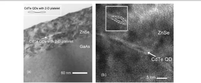
Figure 1. (a) Cross-sectional TEM (XTEM) image and (b) high resolution XTEM image of the CdTe 5.0 MLs QDs. The arrow denotes CdTe
QDs with a two-dimensional (2D) platelet. A schematic diagram of the CdTe QDs and the 2D platelet are shown in the inset.
prediction [4] of the VW growth mode of CdTe/ZnSe SAQDs. On the contrary, this study reports the formation of a two-dimensional precursor layer (PCL) between the CdTe SAQDs and the Se-stabilized ZnSe buffer layer using an alternating supply (AS) method. Cross-sectional transmission electron microscopy (XTEM) proves the existence of the PCL. PL measurements were utilized instead of resonance-PL [8] or PL excitation (PLE) measurements [9] to verify that the PCL was CdSe-like. Furthermore, ground- and excited-state transitions of the CdTe QDs were observed by making PLE and power-dependent PL measurements.
2. Experiments
CdTe/ZnSe SAQDs were grown on semi-insulating epi-ready GaAs(001) using Veeco-Applied EPI 620 molecular beam epitaxy (MBE). Before growth, the native oxide of the substrate was removed by chemical etching with NH4OH and a
thermal desorption process. The ZnSe buffer layer consisted of several mono-layers (MLs) that had been grown by migration-enhanced epitaxy and a layer with a thickness of 50 nm was subsequently grown by conventional MBE. Atomic force microscopy (AFM) measurements indicated that the average roughness of the ZnSe buffer layer was only approximately 0.5 nm. At the end of the buffer layer growth, the Zn shutter was closed and the Se shutter remained open for 5 s to form a Se-stabilized surface. Then, Cd was initially supplied, and the supply was interrupted by opening the Te source using the AS method. The CdTe growth rate was approximately 0.2 ML s−1, as determined by the reflectance spectra and scanning electron microscopic images of the thick CdTe epilayers. The CdTe coverage varied from 0.6 to 1.0, 2.0 and 5.0 MLs. After CdTe deposition, the sample with/without a 50-nm-thick ZnSe capped layer was used for PL/AFM measurement. The AFM image of the 1.0 ML CdTe QDs sample revealed an increase in the surface roughness of the 50-nm-thick ZnSe buffer layer from 0.5 to 1.2 nm. A 325 nm He–Cd laser was used as the excitation source to obtain the PL spectra. A TRIAX-550
spectrometer equipped with a thermal electric cooled photo-multiplier tube was used to analyze the PL spectra. Slit widths were set to 100µm to yield a resolution of better than 1.0 meV. A 300 W xenon lamp with a H10 mono-chromator was used as an excitation source for the PLE measurements.
3. Results and discussion
A bright-field cross-sectional TEM image of the 5.0 MLs coverage sample is shown in figure1. In figure1(a), a two-dimensional platelet associated with CdTe QDs was observed (marked by the arrow). A schematic drawing of the QDs with the platelets is shown in the inset. Note that the existence of the platelet has been verified in several II–VI SK mode QDs systems, such as CdSe/ZnSe QDs [10, 11], CdTe/ZnTe QDs [12], and ZnMnTe/ZnSe QDs [13]. Despite the large lattice mismatch between CdTe and ZnSe, the AS method makes the initial deposition process of Cd atoms on Se-stabilized ZnSe similar to that for CdSe/ZnSe QDs. The thickness of the PCL fluctuates and is discontinuous. It is consistent with aforementioned research in CdSe/ZnSe QDs [10, 11]. Kim et al proposed that the inter-diffusion has an important role in the growth dynamics of CdSe QDs, i.e. the composition of CdZnSe is better than pure CdSe [10]. Figure 1(b) shows a high resolution XTEM. An embedded CdTe QD in a ZnSe matrix with a platelet is clearly observed. The diameter and height of the three-dimensional dot are about 5 and 2 nm, respectively. The planar dot density is estimated to be about 108cm−2from the linear density of figure1(a).
Figure2 presents the PL spectra for CdTe coverages of 0.6, 1.0, 2.0, and 5.0 MLs at 10 K. The near-band-emission (NBE) of the ZnSe buffer layer was found at 2.800 eV. A broad and asymmetric peak was observed at the lower energy side. The peak energy decreased as the CdTe coverage increased, because of CdTe QDs-related emission. The peak energies (marked as open circles) for CdTe coverages of 0.6, 1.0, 2.0, and 5.0 MLs are about 2.654, 2.646, 2.636, and 2.538 eV, respectively. A simple evaluation of the ground state of CdTe QDs by effective-mass approximation [14] reveals that 2
Figure 2. PL spectra at 10 K. Inverted triangles represent emissions
from the CdSe-like two-dimensional precursor layer (PCL) and the phonon replicas (CdSe-1LO and CdSe-2LO). Open circles represent emissions from CdTe QDs. The inset shows the PL excitation spectrum of the 5.0 MLs sample.
a large excitonic blue-shift from the band-gap of bulk CdTe is around 1 eV while the dot diameter is 2 nm. Accordingly, the energies of these peaks significantly exceed the band-gap of bulk CdTe (∼1.580 eV at 10 K), because of the strong quantum confinement that is associated with the large band-offset and small dot size, strain-induced shifts of conduction and valence bands, and the possible inter-mixing between CdTe and ZnSe [7]. In addition, the full width at half maximum (FWHM) increased with CdTe coverage. The FWHM in figure 2(a) is as large as 174 meV, which includes a broad QDs emission and a sharp CdSe-like PCL emission. The broad line shape is attributable to the dot size, the height variation of the 1.0 ML sample is about 1.0 nm by AFM measurement, and the compositional fluctuation. Chang et al calculated that the FWHM of the composition fluctuation in the Zn0.5Cd0.5Te0.5Se0.5epilayer is about 180 meV [7]. Between
the ZnSe buffer and the CdTe QD emissions for the 0.6 and 1.0 ML samples there is another peak near 2.75 eV. This peak is attributed to the emission from the CdSe PCL. Since the lattice mismatch between CdSe and ZnSe is much smaller than between CdTe and ZnSe, a two-dimensional PCL [10,11] can be developed on the Se-terminated surface by irradiating the Cd atoms before the formation of the three-dimensional CdTe QDs by the further deposition of Te atoms. The possible reasons for the large energy shift of the CdSe PCL from the bulk CdSe band-gap are the quantum size effect and the material intermixing between the CdSe PCL and the ZnSe buffer layer. In addition to PL from the CdSe PCL, the longitudinal optical (LO) phonon replicas, labeled CdSe-1LO and CdSe-2LO, were also observed, and the difference between the energies of the phonon replicas is around 30 meV. This is close to the phonon energy, which was measured by the resonance micro-PL and Raman scattering, of the two-dimensional platelet in the CdSe/ZnSe QDs system [8, 15]. The CdTe QDs dot sizes increased with CdTe coverage above 1 ML. Accordingly, the laser-pumped electrons and holes tend to relax to the CdTe QDs of a lower energy state and the emission from the CdSe PCL is suppressed. The PLE
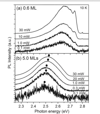
Figure 3. Power-dependent PL spectra of CdTe QDs with (a) 0.6 ML
and (b) 5.0 MLs at 10 K.
spectrum was employed to observe the emission from the CdSe PCL of the 5.0 MLs CdTe QDs sample, as presented in the inset of figure2. The detection photon energy (ED) of the
PLE spectrum was 2.535 eV. The two features at 2.800 and 2.740 eV correspond to the ZnSe NBE and CdSe-like PCL states, respectively.
Figures3(a) and (b) show the power-dependent PL spectra at 10 K for the CdTe QDs of 0.6 ML and 5.0 MLs, respectively. For the 0.6 ML sample with an excitation power of 0.1 mW, only emission from the CdTe QDs was observed, as presented in figure3(a). When the excited power was increased above 1.0 mW, carriers may recombine in the CdSe-like PCL. Moreover, the phonon replica of the CdSe-like PCL emission was observed when the excitation power exceeded 10 mW. Most importantly, the peak energy of the CdTe QDs was independent of the excitation power. This is a characteristic of type-I QDs. In contrast, in figure3(b), the emission of the 5.0 ML CdTe QDs was blue-shifted as the excitation power increased, as plotted using solid circles. This phenomenon is understood as the combined emission of the ground and excited excitonic QD states for larger QDs (5.0 MLs), which is consistent with the previous discussion.
The PLE spectra revealed the existence of the excited state of larger CdTe QDs. Figure4presents the PL spectrum (a) and the PLE spectra (b) and (c) of the 5.0 ML CdTe QDs. A weak peak at 2.494 eV was observed when the PLE was monitored at ED = 2.138 eV (figure4(b)). This peak was attributed to
the first excited state (ES) of the CdTe dots, whose ground state (GS) ED = 2.138 eV. The energy difference between
the GS and ES was about 356 meV. WhenEDwas reduced to
2.067 eV to monitor the emission from larger CdTe QDs, a PLE peak was observed at 2.417 eV. The energy difference between the GS and ES decreases to 350 meV because the quantum confinement is weaker. Accordingly, the broad PL peak in
Nanotechnology 18 (2007) 385602 C S Yang et al
Figure 4. PL excitation measurements of CdTe QDs with 5.0 MLs at
10 K. (a) PL spectrum; (b) and (c) PLE spectra at detection photon energies(ED) of 2.067 eV and 2.138 eV, respectively.
figure2(d) is caused not only by the dot size and concentration fluctuation, but also by the combined emissions of the ground and excited states of CdTe QDs.
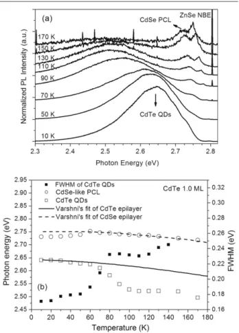
The temperature-dependent PL spectra of a 1.0 ML CdTe QD are shown in figure5(a). The PL peak energies and line widths of the CdSe-PCL and CdTe QDs versus temperature are shown in figure5(b). The open circles and squares represent the peak positions of the emissions from the CdSe-PCL and CdTe QDs, respectively. The solid and dashed lines represent Varshni’s fits to the energy gaps of the CdTe and CdSe epilayers, respectively. The peak energy of the CdSe-PCL follows the dashed line, which corroborates the assignment of a CdSe-like PCL rather than a CdTe-like PCL. At low temperature, the data points are slightly below the dashed line, implying the existence of a PCL localized state [16]. CdTe QD emission is consistent with Varshni’s fit for the CdTe epilayer (solid line) below 60 K. At over 60 K, a significant red-shift occurs due to the thermally activated transfer of carriers from the smaller CdTe QDs to the larger CdTe QDs through the CdSe-like PCL or the ZnSe matrix. As the temperature increased above 140 K, the PL was thermally quenched and the peak energy decreased monotonically as the temperature increased. However, Chang et al noted that the peak energy of CdTe QDs increased with temperature due to the existence of a localized state at a temperature exceeding 150 K [7]. This significant discrepancy implies that no localized state related emission could be observed in our QDs. In addition, the growth mode found in [7] was identified as the VW mode; the PL peak energy of their CdTe QDs fitted to the CdTe bulk Varshni’s curve. In this study, the strong red-shift implies the existence of a PCL [17] and growth by the SK mode. Below 80 K, the FWHM (solid squares) of the CdTe QD emission exhibits monotonic broadening as the temperature increases. As the temperature increased above 80 K, the FWHM exhibited initial narrowing followed by broadening, due to the initial transfer of carriers from the smaller to the larger dots, and the subsequent thermal electron–phonon coupling. These are typical phenomena of SK QDs with a wetting layer [17,18].
Figure 5. (a) Temperature-dependent PL spectra of 1.0 ML CdTe
QDs. (b) Variation of PL peak energy (open circles and squares) and full width at half maximum (solid squares) of 1.0 ML CdTe QDs with temperature. The solid and dashed lines represent Varshni’s fits with the energy gaps of the CdTe and CdSe epilayers, respectively.
4. Conclusion
In summary, this investigation establishes the existence of a CdSe-like PCL between the CdTe QDs and the Se-stabilized ZnSe buffer by XTEM and PL measurements. The PLE measurements reveal the presence of the first excited state in the larger CdTe QDs. The temperature-dependent PL spectra of the 1.0 ML CdTe QDs demonstrate that the thermally activated carriers are transferred from the smaller QDs to the larger QDs through the CdSe-like PCL.
Acknowledgments
This work was supported by MOE-ATU, and the National Science Council under grant numbers NSC 95-2112-M-009-047 and 95-2112-M-033-008-MY3, and the Center-of-Excellence Program on Membrane Technology, the Ministry of Education, Taiwan. The authors are grateful for the support from the National Nano-Device Lab.
References
[1] Lin T Y, Lyu D Y, Chang J, Shen J L and Chou W C 2006
Appl. Phys. Lett.88 121917
[2] Lee M E, Yeh Y C, Chung Y H, Wu C L, Yang C S, Chou W C, Kuo C T and Jang D J 2005 Physica E26 422