Invited Paper
Holographic
polarization-selective elements in optical network applications
Yang-Turig Huang, Meng-Fu Lin, Jiun-Shiou Deng, Kai-Tirig Fan, and Mu-Jung Cheri Department of Electronics Engineering and Institute of Electronics
National Chiao Tung University, ilsinchu, Taiwan, Republic of China
ABSTRACT
Highly polarization-selective holographic elements can be achieved with suitable designs. The presented holographic polarization-selective elements are compact and light-weight, and the fea-ture of normally incident and output coupling provide better flexibility and easier alignment for system applications. With suitable designs and arrangements, these elements can be combined to implement star couplers to distribute equal optical power from each input channel to all output
channels. In addition, based on our holographic polarization-selective elements with electro-optic halfwave plates, holographic polarization-dependent and polarization-independent optical switches are introduced. The structures to use these switches in various compact three-dimensional multi-stage interconnection networks for reconfigurable interconnections and in self-healing rings (SHR) for network service restoration are presented.
Keywords: holographic optical elements, polarization beam splitters, optical networks, wavelength-division multiaccess, star couplers, optical interconnection networks, protection rings.
1. INTRODUCTION
Volume-type holographic optical elements perform polarization-dependent l With suitable designs, highly polarization-selective holographic elements can be achieved, and these
corn-ponents have been designed and fabricated.28 In this presentation, we first review the basic struc-ture of our holographic selective elements. Based on our holographic selective elements with electro-optic halfwave plates, we also introduce holographic polarization-dependent and polarization-inpolarization-dependent optical switches.
In a wavelength-division multiaccess (WDMA) network passive star couplers are important
elements. The function of a star coupler is to distribute optical power of each input beam
asso-ciated with a unique wavelength equally to all outputs with their respective tunable receivers.9"0 With suitable arrangements, our holographic polarization-selective elements can be used to imple-ment polarization-dependent and polarization-independent star couplers. With holographic optical switches to implement various three-dimensional multistage interconnection networks for reconfig-urable interconnections are also discussed.114 In addition, we apply our polarization-independent holographic optical switches in a self-healing ring with passive protection ring (SHR/PPR) for ser-vice survivability in synchronous optical networks (SONET).15'16 All of our deser-vices are compact and light-weight, and the feature of normally incident and output coupling provide better flexibility and easier alignment for system applications.
2. HOLOGRAPHIC POLARIZATION-SELECTIVE ELEMENTS
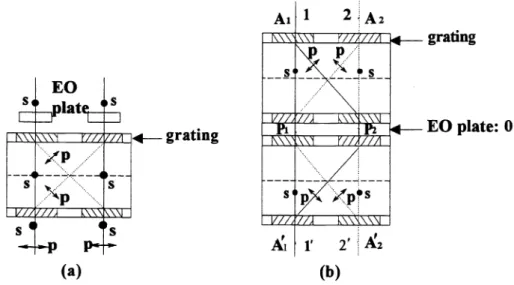
The basic structure of our holographic polarization-selective elements is shown in Fig. 2_8 Two symmetric polarization-selective grating pairs are formed on two sides of a dielectric substrate.
The diffraction angle in the film medium is 9D, and the Bragg reconstruction input angle is 00, i.e.
the input beam is normally incident on the device. On the other hand, in the output coupling, the reconstruction angle is 9D and the output diffracted beam is also normal to the device as
shown in Fig. 1. Based on Kogelnik's coupled wave theory,1 the diffraction efficiencies of s- and
p-polarization fields with respect to the grating plane for each grating, r and i,,arerespectively
given as
— . 2 rn1d
_
. 2rmldVcos9Dlls—Slfl , ?7—S1fl 1
\\/cosOD A
where A is the operating wavelength, d is the thickness of the grating film, and n is the index modulation of the grating, respectively. From the above equations, suitable values for 9D and
nid/A can be solved as shown in Table 1 to obtain high polarization-selective property (0%- and 100%-diffraction for s- and p-fields, respectively; or 100%- and 0%-diffraction for s- and p-fields, respectively), and these devices have been designed and some were fabricated.28
Using s-transmission/p-diffraction gratings in the structure shown in Fig. 1 as an example,
when the input beams are s-polarized, the device will perform the function of straight connections
(direct transmission) as shown by the solid connection lines in the figure. On the other hand,
when the input beams are p-polarized, the device will perform the function of swap connections
(diffraction) as shown by the dashed connection lines. (For s-diffraction/p-transmission gratings, this holographic polarization-selective element will perform s-swap/p-straight function.)
3. STAR COUPLERS USING HOLOGRAPHIC POLARIZATION-SELECTIVE ELEMENTS 3.1 Polarization-dependent star couplers
A basic 2 x 2 coupler with our holographic polarization-selective elements to construct our
polarization-dependent passive star coupler is operated as shown in Fig. 2. When the polarization
of light from the laser source is specified, the polarization of input light is arranged such that it has the same amount of s- and p-components with respect to the grating planes, i.e., 45° with respect to the x- and y-axes as shown in the figure. Two input signals from channels 1 and 2
with wavelengths of A1 and A2, respectively, are normally incident on the device. Since the device performs s-straight/p-swap connection, s-and p-components of signals with wavelength A1 from channel 1 will be equally distributed to channels 1' and 2', respectively. On the other hand, p- and s-components of signals with wavelength A2 from channel 2 will be equally distributed to channels 1' and 2', respectively. This 2 x 2 coupler is the basic unit to form our holographic star couplers.
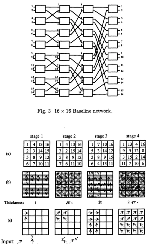
In order to implement a star coupler, an efficient N x N connection network is also required.
A 16 x 16 baseline interconnection network for our one design example is shown in Fig. 3•14 Based on the baseline network structure and channel number assignment illustrated in Fig. 3, we can
obtain a table to describe channel connection relations between stages as shown in Table 3. From these connection relations, we determine mapping tables of all stages as shown in Fig. 4(a). The numbers of these mapping tables indicate the corresponding input channel numbers of all stages. For example, the output of channel 1 at stage I is connected to the input of channel 1 at stage 2, whereas the output of channel 2 at stage 1 is connected to the input of channel 3 at stage 2. In these mapping tables each channel pair to form a coupler is at 45° with respect to the corresponding pair of the preceding stage. In this case, the polarization of the output optical field of each channel is at 45° with respect to the input grating plane of the following stage, and the optical power can be equally distributed to two output channel through the coupler as shown in Fig. 4(b) and (c).
Fig. 4(b) shows the grating pairs for all couplers at all stages. Each two-end arrow represents
a grating pair of a coupler corresponding to the channel numbers in Fig. 3. Each quantity in the SP!EVol. 2885 / 113
tables represents the output power ratio compared to the input power of the first stage. In this
power distribution description example, we only couple an optical power into the input of channel 1 at the first stage. The corresponding polarizations of input and output optical fields of all stages
are shown in Fig. 4(c). In this figure, x'- and y' axes are at 45° with respect to x- and y-axes.
When an optical field with a unity power and the polarization at x'-direction is incident to channel 1 of the first stage, then the power of 1/2 is distributed to output channel 1 with the polarization at x-direction and 1/2 to channel 2 at y-direction, and goes to input channels 1 and 3 of the second stage. Through the couplers at the second stage, the power of 1/4 is distributed to channels 1,2,3,4, and the corresponding input channel numbers of the third stage are 1, 3, 5, 7. Through the third stage, the power of 1/8 is distributed to channel 1, 2, .. . , 7,8, and the corresponding input channel
numbers of the fourth stage are 1 ,3,.. . , 11,13. Finally, through the fourth stage, the power of 1/16 to each channel is equally distributed to channels 1—16 as shown in the figure, and the function of a star coupler is achieved. Optical fields with the polarization at x'-direction incident to other channels will follow the same process to equally distribute the power to all channels through the whole star coupler. As shown in Fig. 2, the required thickness of a coupler is proportional to the distance between the centers of two coupled channel, and the corresponding thicknesses t, 2t, and2v't for all stage layers are also shown in Fig. 4(b). When grating pairs are fabricated with the corresponding substrate thickness as shown in 4(b), all suitable coupler layers are formed. Stacking
all layers in order as shown in the figure, a compact holographic star coupler with no interconnection
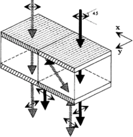
lines is built. To view the three-dimensional structure of this device for easy understanding. the three-dimensional configuration for a 4 x 4 star coupler composed of two stages of holographic polarization-selective elements is illustrated in Fig. 5.
The procedures to design a passive star coupler using our holographic polarization-selective elements can be summarized as:
(1) Determine an efficient connection network, such as a baseline network in our case shown in
Fig. 3, based on 2 x 2 coupler, where i-th (odd number) and (i + 1)-th channels form a pair of 2 x 2 coupler at each stage to equally distribute optical power from one input channel into two output channels as shown in Fig. 2.
(2) Determine the channel connection tables from the network connection structure as shown in
Table 3.
(3) Assign input channel numbers of hologram set for each stage to form mapping tables as
shown in Fig. 4(a). Each pair must be maintained at 45° with respect to the pair of the
same designated channel numbers of the preceding stage such that optical power at the input of each channel can be equally distributed into two channels with two different (s-andp-)
polarizations through one 2 x 2 holographic coupler as shown in Fig. 2.
(4) Determine the orientation of each grating plane pair based on the rule that i-th (odd number) and (i + 1)-th channels form a pair at each stage, and determine the corresponding thickness of the polarization beamsplitter set for each stage, which is proportional to the center distance of the grating pair as shown in Fig. 4(b).
(5) Follow the mapping tables to stack all stages in order, a compact holographic star coupler with no connection lines between stages is constructed.
3 .2 Polarization-independent star couplers
In some applications such as fiber optic communications, the input light of a star coupler might not be linearly polarized. In this case, the above polarization-dependent star coupler is not suitable. Therefore, we need to design polarization-independent star couplers for this kind of applications.
The proposed method is to add one more stage in front of the first stage of the original
polarization-dependent star coupler and with a grating structure the same as the original sec-ond stage (45° with respect to the original first stage) such that the input beams can be splitted
to two orhogonal polarized fields and both these two orthogonal polarized fields can be equally distributed to all output channels through the original polarization-dependent star coupler. There-fore, all output channels obtain equal optical power for both two orthogonal polarized fields. Fig. 6 shows the polarization of the fields and the power distribution process is illustrated. As shown
in the figure, x and y are the unknown proportions for two orthogonal polarizations of an input
beam. and splitted to two directed channels after passing the first stage. For a N x N star coupler with log2P + 1 stages, the output power for each channel is about (x + y)/N (for a low-loss case). The power distribution process for a 16 x 16 star coupler is illustrated in Fig. 6.
4. HOLOGRAPHIC OPTICAL SWITCHES 4.1 Polarization-dependent optical switches
2 x 2 switch is a basic unit for multistage switching networks12t4 and protection rings in
optical communications.'5'16 Basically, a polarization beam splitter (PBS) in conjunction with an electro-optic halfwave can form this type of optical switch. Wollaston and Rochen prism cubes are conventionally used for polarization beamsplitting. Our holographic polarization-selective elements
can be used to replace conventional prism cube PBSs in switching applications.27 The typical unidirectional polarization-dependent holographic optical switch with our structure is shown in Fig. 1. These type switches are used only for specified linearly-polarized input beams (s- or p-polarization with respect to the grating planes). In the example shown in the figure, the input
beams are s-polarized. When the electro-optic half plate is inactive (state 0), the switch performs
the straight connections (solid lines); when the plate is active (state 1), the fields are rotated by
450andthe device performs the swap connections (dashed lines). 4.2 Polarization-independent holographic optical switches
Polarization-independent optical switches with electro-optic halfwave plates and polarization beamsplitting prisms have also been investigatedJ7'18 The structure we propose for a
polarization-independent holographic optical switch is shown in Fig. 7(b). This switch is composed of an
electro-optic halfwave plate sandwiched by two holographic polarization-selective elements. In this example the gratings perform s-transmission/p-diffraction functions. For convenience of discussion, we denote six positions on the connection paths by points A1, A2 (corresponding to channels 1 and
2), P1, P2 (corresponding to plate positions), and A, A (corresponding to channels 1' and 2').
The inactive state (State 0) of the electro-optic halfwave plate will make the switch perform the function of bidirectional straight connections (1 -+1', 2 2')as shown in Fig. 7(b). In the other case, i.e., when the electro-optic halfwave plate is active (State 1), the field polarizations will be changed after passing through the plate, and the electro-optic halfwave plate will make the switch perform the function of bidirectional swap connections (1 -+2',2 -+1'). All connection states are also clearly shown in Table 2.
For s-diffraction/p-transmission gratings, the holographic polarization-selective element in Fig. 1 will perform s-swap and p-straight beam splitting functions. However, the structure of Fig. 7 with
s-diffraction/p-transmission holographic PBS's can provide the same 2 x 2 bidirectional
polarization-independent switching functions as with s-transmission/p-diffraction holographic PBS's. The oniy difference is that the propagation paths of s-andp-polarization fields are interchanged within this
switching device.
5 . MULTISTAGEINTERCONNECTION NETWORKS
WITH HOLOGRAPHIC POLARIZATION-SELECTIVE ELEMENTS
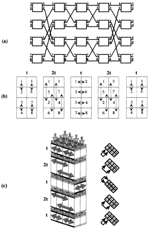
Benes network is a classical multistage nonblocking interconnection network and the its fabric for a 8 x8network is shown in Fig. 8(a).11 When we build these networks with use of holographic optical switches, the fixed interconnection lines between stages must be considered. Instead of using additional elements to change propagation directions of light beams after each stage for
these fixed interconnections, we employ two-dimensional input channel layouts and implement the connections between stages by appropriate grating-orientation arrangement of each switching units at each stage. Then the network can be constructed by piling up those elements. Fig. 8(b) shows the mapping tables for channel interconnection numbers between stages as described Section 3.
Channels 1, 2, 3, 4, 5, 6, 7 and 8 at stage 1 are connected to 1, 5, 2, 6, 3, 7, 4, and 8 at stage
2, respectively. Each arrow "—÷" denotes
the switching relation by a 2 x 2 switch unit. The
relative thickness t, 2t, t, 2t or t of the substrate glass for each stage is also shown in the figure.
Three-dimensional structure with our holographic optical switches is shown in Fig. 8(c). The
unidirectional networks consisting of unidirectional switching units can be changed to bidirectional networks just by adding a layer of electro-optic half-wave plate at the output end.
6. APPLICATION OF HOLOGRAPHIC OPTICAL SWITCHES
TO SONET SELF-HEALING RINGS
A self-healing ring, which is a ring network that provides redundant network equipment and/or bandwidth so that disrupted services can be automatically restored, is one of the restoration tech-niques for service survivability.'6 In a synchronous optical network (SONET), an SHR is totally
automatic and provides complete restoration capability for a single fiber cut or equipment
fail-ure. It can also provide some survivability for hub digital cross-connect system (DCS) failures and major hub failures (e.g., flooding or fires). This self-healing capability is commonly offered by a second communication ring parallel to the first working ring as shown in Fig. 9. In the figure, the add-drop multiplexers (ADMs) are the multiplexing devices that add and drop local channels and pass through transit channels.16 The hub in this ring provides an access point to another network for central offices (COs). A self-healing ring with passive protection ring is composed of two parts: a SONET ring for working signals and a totally passive protection ring for protection signals. The passive protection ring is a standby ring dedicated to the working ring.
Polarization-independent holographic optical switches shown in Fig. 7 can perform protection
switching in a self-healing ring by both line switch and loopback functions. In addition, both fiber failure and node failure can be retrieved here. Fig. 9(a)-(c) illustrates the scenarios of no failure, fiber failure between two nodes, and node failure, respectively, where the loopback function
is utilized. The fiber failure scenario using the line switch function is depicted in Fig. 9(d). In Fig.
9(b), there is a break in both rings between CO1 and CO2. The 2 x 2 optical switches OSB in
CO1 and OSA in CO1 change their states to "swap" connections. Then a new ring is formed and
the ring network is restored. If node failure occurs as shown in Fig. 9(c), both optical switches
OSB in CO1 and C03 change their states to "swap" connections and a new ioop is set up. If only 116/SPIE Vol. 2885
the working fiber is broken as shown in Fig. 9(d). the protection approach of line switch can be
exploited. In this case, all optical switches alter their functions and the whole protection fiber
serves as the working fiber temporarily.
7. SUMMARY
In this presentation, the basic structure of our holographic polarization-selective elements are reviewed. With suitable designs and arrangements, these elements can be combined to implement polarization-dependent and polarization-independent star couplers to distribute equal optical power from each input channel to all output channels. Based on our holographic polarization-selective elements with electro-optic halfwave plates, holographic dependent and polarization-independent optical switches are discussed. The structures to use these switches in various compact three-dimensional multistage interconnection networks for reconfigurable interconnections and in
self-healing rings (SHR) for network service restoration are presented. All of our devices are compact and light-weight ,andthe feature of normally incident and output coupling provide better flexibility and easier alignment for system applications.
8. ACKNOWLEDGEMENT
This work was supported by the National Science Council of the Republic of China under contract NSC86-22 15-E-009-055.
References
1. H. Kogelnik, "Coupled wave theory for thick hologram gratings," Bell Sys. Tech. J., vol. 48,
no. 9, pp. 2909—2947, Nov. 1969.
2. M. Kato, H. Ito, T. Yamamoto, F. Yamagishi, and T. Nakagami, "Multichannel optical switch
that uses holograms," Opt. Lett., vol. 17, no. 11, pp. 769—7'71, June 1992.
3. Y.-T. Huang and Y.-H. Chen, "Polarization-selective elements with a substrate-mode grating pair structure," Opt. Lett., vol. 18, no. 11, pp. 921—923, June 1993.
4. Y.-T. Huang, "Polarization-selective volume holograms: general design," Appi. Opt., vol. 33,
no. 10, pp. 2115—2120, April 1994.
5. Y.-T. Huang and Y.-H. Chen, "Optical switches with a substrate-mode grating structure," Optik, vol. 98, no. 1, pp. 41—44, Nov. 1994.
6. J.-T. Chang, D.-C. Su, and Y.-T. Huang, "Substrate-mode holographic polarization-division
multi/demultiplexer for optical communications," Appi. Opt., vol. 33, no. 35, pp. 8143—8145,
Dec. 1994.
7. Y.-T. Huang "Polarization-independent optical switch composed of holographic optical
ele-ments," Opt. Lett., vol. 20, no. 10, May 15, 1995.
8. J.-T. Chang, D.-C. Su, and Y.-T. Huang, "A four channel polarization and wavelength separa-tion element using substrate-mode stacked holograms," Appi. Physics Lett., vol. 68, no. 25, pp.
3537—3539, 1996.
9. I. P. Kaminow, P. P. Lannone, J. Stone, and L. W. Stulz, "FDM-FSK star network with a
tunable optical filter demultiplexer" ,ElectronicsLett., vol. 23, pp. 1102-1103, 1987.
cz
7°A3IdS/911 suotpauuozdig
,j+—
11V'd
V
—--d
4—ry
Zy(Atpe)
I+
j
VdtV
'd
ZytV
suo!puuo
1Z ci cid
V
—r
v
(Atpur)
0,T—I
d
ty
ty4__td__ty
uoicpunj P1MSes
°'°D
tjd
rus
aip uoU0!Z1I0d
PTa!daes
aTd
SfiSllIV1IEMoII3VJdIU/MoIsSHAsNV'llI-S
HuM
HDJJMS TIVDIIdO DIHdYUOOIOH1NNadcIMIMOIuvZn1vnIOd
dO SLVILS NOIJLDNNOD:
[\TJJ
LI
T
LOLy/ptu
0VTT7O09
cr6 %00I %0 %OOT d[ %0 %00T %0 iLd
J
IL JLS
sDMIIV'aDAIIDaTIas-MoIuvzn1vTrod
JO
Sf1IYA
:
TIHV
66I
auttç 'SIL—ILdd
'9
0u'
J0A'd7
•lotltpaLL uoioz/jjsAiz
prnbrreuxau
posi
jo
pasodmo
pps
pdo
xjssoi-o'j,.
'!!cd
A 8166I
qa
'S0—90 dd •ou'ç
10A'7
•lOUZId6LL •UOlOZIcf¶[I
A'!!cd
xi3!do
ips
pasodwoDjo
wau
p!nbH 'sTIa3L1
66T
'UOSO
'asno}jJ3aJv
'11iiqvainindzaLs
JoaN
Z[
'rLMH-J
91 0661 qaj '6cT—I dd'
•ou'
J0AZ/df
acwTip/57f
¶3J
'9a1ptMs TD!d0uisn
aincappre
ioau
iaq
aApaJp-so
aqArAJnse u!uireTd
ioj
saojouipa
pu
sa!aeJs,,
'q!qH
.d
Sv"
M
11-1i
UT1JDJMS¶I
9UaLJ UO 'UflULULULOQ TOA'
0U '01 dd'6LI0TLI
P0
0661ctuooijd pue
uoJpaJa
paads-itt
u
suorDqdde
J!aTfl pire S)JOMOU N0T-!TflI'\I,, a'T[1-3
N
886T daS 'I0—LT0 dd '01 °' 'L 10A 'ldO ctdV'suxass
lossaDoJdtlInw aeDs-areJ ioj sjJoau aesqjnm iezndO,,'as
aj
v
9S6Tuf
'—0
dd'
ou 'L JOA'yzd
snq T!dO,, 'uuuxTToJy
c961'T°A
MM 'DtuIap'eDV'10aN
flUilddtLUO3 Jo Pt4O2t/1 lIXfliV WDIIJ 'sauaH'
A TI66I
ny
'çc-9
dd'gj
¶7T'rJ'UflpJMS
UI S3iUOO1j,, 'UOUill S H 0TTABLE 3: CHANNEL CONNECTIONS BETWEEN STAGES OF A BASELINE NETWORK Output channel of 1st stage
—* Inputchannel of 2nd stage
Output channel of 2nd stage
—Inputchannel of 3rd stage
Output channel of 3nd stage
— Input channel of 4th stage
1— 1+2x0= 1
2— 1+2x1= 3
1— 1+2x0= 1
2— 1+2x1= 3
3
1+2x2= 5
4—41+2x3= 7
1—1+2xO= 1
2—1+2x1= 3
31+2x2=
54—1+2x3=
75—1+2x4= 9
6—1+2x5=11
7—1+2x6=13
81+2x7=15
3 2+2x0= 2
4—?2+2x1= 4
5—4 5+2x0= 56—
5+2x1= 7
5— 2+2x0= 2
6—+2+2x1= 4
7— 2+2x2= 6
8
2+2x3= 8
7—4 6+2x0=
68
6+2x1= 8
9—? 9+2x0= 91o— 9+2x1=11
9— 9+2x0= 9
1O—+ 9+2x1=11 11—v9+2x2=13
12—9+2x3=15
9—+2+2x0= 2
1O—2+2x1= 4
11—+2+2x2=
612—+2+2x3=8
13—2H-2x4=1O
14—2-F2x5=12
15—2+2x6=14
16—+2+2x7=16
11—+1O+2x0= 10
12—1O+2x1=12
13—13+2xO=13
14—13+2x1=15
13—÷1O+2x0=1O
14—1O-F2x1=12
15—+1O+2x2=14
16—+1O+2x3=16
15—14+2xO=14
16—14+2x1=16
>i' P4 S\Lr77
•..P4
---
p /i'kI\\
>p P4<*
Fig. 1 The structure of a holographic polarization-selective element.
Fig. 2 The structure of a 2 x 2 coupler to construct holographic star couplers.
Fig. 3 16 x 16 Baseline network.
stage 1 stage 2 stage 3 stage 4
1 4 13 16
1 4 13 16
1t7 10 16
1 13 4 1
2 3 14 15
3 2 15 14 T3
14 12 9 5 12 81 (a) —I58912
58912 28915 315214
671011
761110 641311 117106
2t 24'tv'
(b) Thickness: t (c) Input:,
Fig. 4 Power distribution process of a 16 x 16 star coupler. (a) Mapping tables.
(b) Grating orientations, device thicknesses, and power distribution ratio. (c) Output field
polarizations at each channel.
Fig. 5 Three-dimensional structure of a 4 x 4
polarization-dependent star coupler.
added stage 1
stage 2x+ y< 1 (Power Ratio) (Thickness)
Fig.
6 Grating orientations, device thicknesses and power distribution ratio at each stage
of a 16 x 16 polarization-independent star coupler.
Ai 1
2A2
grating 1777 777\\ ri/VIA
vz I/A \\\\N— EO
plate: 0 SPIE Vol.2885 / 121F
stage 5t
wx/4y142t
2 4
S 5(a)
Ai 1'2'A'2
(b)Fig. 7 The structure of a holographic optical switch s-transmission /p-diffraction
grat-ings. (a) Unidirectional dependent switch. (b) Bidirectional
t
2t 1 3 (a) (b) (c)2t
/t"
t
2t
t
2t
t
S
Fig.
8 8 x 8 Benes interconnection network. (a) Network fabric. (b) Mapping tables. (c)
Three-dimensional structure with holographic optical switches.WF: Working Fiber PF: Protection Fiber
CO : Central Office ADM: Add-Drop Multiplexer
OS: Holographic Optical Switch
Fig. 9 SHR/PPR using two holographic optical switches at each node (a) Normal
opera-tion. (b) Fiber failure between two nodes. (c) Node failure. (d) Working fiber failure.
SPIE Vol.2885 / 123 switch
(a) (b)