This content has been downloaded from IOPscience. Please scroll down to see the full text.
Download details:
IP Address: 140.113.38.11
This content was downloaded on 28/04/2014 at 12:07
Please note that terms and conditions apply.
Electrical Characteristics of CO2-Sensitive Diode Based on WO3 and IrO2 for Microsensor
Applications
View the table of contents for this issue, or go to the journal homepage for more 1998 Jpn. J. Appl. Phys. 37 L245
(http://iopscience.iop.org/1347-4065/37/2B/L245)
Jpn. J. Appl. Phys. Vol. 37 (1998) pp.L245–L247 Part 2, No. 2B, 15 February 1998
c
°1998 Publication Board, Japanese Journal of Applied Physics
Electrical Characteristics of CO
2-Sensitive Diode Based on WO
3and IrO
2for Microsensor Applications
Shuchi CHAO
Department of Electrophysics, National Chiao-Tung University, Hsin-Chu, Taiwan, ROC
(Received October 22, 1997; accepted for publication December 26, 1997)
Devices based on the contact of sputtered WO3and IrO2that are covered by an HCO−3-containing polymer exhibit reversible and reproducible CO2-dependent, diodelike current rectification at 1 atm and room temperature. The gain or loss of current in the forward direction as a function of CO2concentration is found to be tunable by controlling the thickness ratio of the WO3 and IrO2films. The rectification mechanism is uniquely governed by the thermodynamic free energies; this is the key to the durability previously not attainable using conventional diodes in microsensor applications. These diodes are useful as a basis of construction for durable microsensors operating in gases or liquids.
KEYWORDS: diode, microsensor, CO2, rectification, sputtered WO3, IrO2
port of charge across the WO3/IrO2interface is allowed only in the forward direction and forbidden in the opposite direc-tion. The current growth in the forward direction can occur readily via the thermodynamically favored reduction of IrO2 by the reduced HxWO3. In fact, the attenuation of current in the reverse direction is more an indication that the ox-idation of Ir(OH)3 by the oxidized WO3 is thermodynami-We present a new diode as a basis of construction for fab-ricating durable microsensors that are operable in gases and liquids at 1 atm and room temperature. The device is based on pH-sensitive WO3and IrO2, which interact with H+in the reversible redox reactions,1, 2)
WO3(bleached) + xH++ xe−↔ HxWO3(colored), and (1) IrO2· (H2O)(colored) + H++ e− ↔ Ir(OH)3(bleached).
(2) Both WO3 and IrO2 reductions to the conducting HxWO3 and insulating Ir(OH)3occur at more positive electrochemi-cal potentials in acidic media over a range of pH values be-tween∼2-123, 4) (reactions (1) and (2)). These redox
trans-formations arise due to the insertion of ionic species into the oxides, which can produce large conductance changes.4, 5)
The present work is inspired by the earlier discoveries in this laboratory that a bicarbonate (HCO−3)-doped, polyvinyl al-cohol (PVA) solid polymer matrix interfaced with WO3 or IrO2, can respond to CO2 in terms of resistance or potential across closely spaced microelectrodes at 1 atm and room tem-perature.6, 7)Despite the advantages of such relatively simple chemical-sensitive resistors and potentiometers, practical use is less attractive due to the lack of a built-in current “turn-on” capacity commonly found in diode and transistor-based microsensors.8) However, WO3 and IrO2 are known to be
complementary cathodic and anodic electrochromic materi-als,9)and have been used to demonstrate optical attenuation.
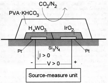
By connecting WO3 and IrO2 in series, as shown in Fig. 1, both oxides become conducting under positive bias in the forward direction and insulating under negative bias in the reverse direction. However, the device function cannot be fully explained by treating the oxides simply as variable series resistors. Since HxWO3/WO3 is cathodically electroactive whereas Ir(OH)3/IrO2 is anodically electroactive, the
trans-cally not feasible. In our view, this type of rectification gov-erned by thermodynamic free energies is the major advantage for constructing such diodes based on the contact of WO3 and IrO2. The devices will be durable since they are made of robust materials. Unlike previous microsensors based on conventional or organic diodes,8, 10)their electrical functions in gases and liquids are not susceptible to the environmen-tal variabilities arising from interfacial or material instability. Exploratory experiments in this area have led to our results that the electrical contacts of solid WO3and IrO2films, sput-tered on adjacent Pt electrodes and covered by the polymer blend PVA·KHCO3 (Fig. 1), can be used to generate diode-like current-voltage outputs that respond to CO2 changes in the atmosphere.
The Pt-pad electrodes in Fig. 1 are fabricated using simi-lar procedures as described earlier.6)The electrodes are
typi-cally 290 µm wide and 580 µm long (excluding the lead por-tion) and are separated by a distance of 480 µm. To avoid annealing the IrO2due to heating by subsequent WO3 depo-sition, sputtering of the WO3target (99.99%, Pure Tech) at radiofrequency is carried out first under 20% O2 in Ar at a total pressure of 90 mTorr, in the same apparatus as used be-fore.7)A Si wafer with micromachined V-grooves is used as
Fig. 1. Scheme showing the forward-biased diode based on the contact of WO3and IrO2on Si under CO2modulation.
the deposition mask. The mask and devices on the wafer are pressed onto a heated substrate platen at 676 K.3)The WO
3 films exhibit broad cyclic voltammograms in aqueous 1.0 M HClO4over the potential range of 0.3 to−0.3 V vs a saturated calomel electrode, as reported previously.3)Characterization
of the films on indium-tin oxide glass shows electrochromism in the visible region and a wide range of absorption change under potential cycling in aqueous 1.0 M H2SO4. The change is∼15–85% in transmittance at 650 nm, near the wavelength of maximum difference in the absorption band. The pro-cess for derivatizing the Pt electrode with the amorphous IrO2 film, next to the WO3film (Fig. 1), by the reactive sputtering method and the characterizations have been described ear-lier.7) The prepared WO3 and IrO2 films are robust and ad-here strongly to the Pt surface. No difficulty such as peeling has been encountered throughout the course of our experi-ment. After deposition of the oxide films, electrical contact of individual Pt electrodes is made using Ag epoxy, which is later encapsulated using insulating epoxy. Next, the whole de-vice active area is covered with the polymer blend, polyvinyl alcohol (PVA, average molecular weight=1.33× 10⁵g/mol) with potassium bicarbonate (Fig. 1). The polymer blend, PVA·KHCO3,7)used for creating a CO2-modulated pH
envi-ronment for the diodes, is ready for use as an aqueous solution with 0.06 mM of PVA and 2 mM of KHCO3. No other sup-porting electrolyte has been added since the polymer blend functions only as a source or sink for H+, and not as an electrolyte to carry ionic current. After evaporation of H2O at 35◦C for 24 h, the cured polymer blends form transparent films that are highly adhesive to WO3and IrO2. No peeling or fogging of the films has been encountered throughout the electrical and light transmission experiments. The current-voltage sweeps are generated using a Keithley 236 source-measure unit (Fig. 1). The relative transmittance through the optical-quality oxide films is measured by reflection off the Pt surfaces on which the films are deposited, Fig. 1. Since colored IrO2films show featureless transmission in the vis-ible region7) and colored HxWO3 films show the optimal
absorption difference near 650 nm, a stabilized He–Ne laser (632.8 nm) is used as the light source. Optical microscopy re-veals that uniform bleaching and coloring can occur in each of the oxide films on Pt. As shown in Fig. 1, each film has only one underlying Pt electrode. This forces the potential drop to be confined to the WO3/IrO2 interface, leaving the individual films on Pt approximately at equipotential and of the same color. Light is chopped and split for simultaneous focusing onto one Pt surface within the diode sample (Fig. 1) and a second Pt surface that is oxideless within a specially made “diode” reference blank. The reflected beams are each collected by a detector (UDT 10DP) whose photocurrents are ratioed by lock-in amplifiers (Stanford 830) to obtain the rela-tive transmittance as a function of the bias voltage. When the CO2atmospheres are needed, the diodes packaged into inte-gral flow cells are used, as earlier.11) The %CO2 concentra-tion in N2and the %H2O saturation conditions are generated as described earlier.11)
The current-voltage characteristic of diodes based on WO3 and IrO2are shown in Figs. 2 and 3. The CO2gas creates a pH-regulated environment for the diodes (Fig. 1), through its pH-lowering effect, as previously reported.7)It equilibrates in
the bicarbonate-blended polymer PVA·KHCO3according to
the dissociative reaction
(CO2+ H2O↔)H2CO3↔ H++ HCO−3 ↔ 2H +
+ CO23−. (3) It has been established in this laboratory7) that the pH in
PVA·KHCO3can be reversibly modulated using CO2gas. It has also been determined that this pH is proportional to the negative logarithm of the concentration of CO2, -log[CO2], to which PVA·KHCO3is exposed. Accordingly, changing -log[CO2] in the atmosphere in Fig. 1 is, in effect, equivalent to linearly shifting the pH in the PVA·KHCO3coating of the diode. As the results of the CO2-dependent experiment in Fig. 3 show, diodes based on WO3and IrO2 undergo a
cur-Fig. 2. Typical diode current-voltage characteristics and the relative trans-mittance changes in the oxides under 1% CO2in N2at 1 atm, 298 K and
100% H2O saturation.
Fig. 3. The current in the forward direction under CO2 modulation at
1 atm, 298 K and 100% H2O saturation.
Jpn. J. Appl. Phys. Vol. 37 (1998) Pt. 2, No. 2B S. CHAO
rent decrease in the forward direction when the CO2 concen-tration is increased within the range of 1–100% in N2. In the inset in Fig. 3, the voltage at which an arbitrary small current (1.4 µA) in the forward direction is derived, VSC, is plotted vs
-log[CO2] for each of the CO2-dependent I/V curves. The observed proportionality reveals that VSCof the diode is also
proportional to the pH in the diode environment. These re-sults are consistent with the WO3 and IrO2 redox processes (reactions (1) and (2)). The electrochemical potentials in both reactions become more positive in more acidic environments. This shift can be considered to result from the pH-dependent changes in the potential drop across the Helmholtz layer at the surface of both oxides, as stated earlier.6, 7)On the
poten-tial scale, the shifting of redox potenpoten-tials towards the positive region renders reductions more favorable than oxidations un-der fixed driving force. When the bias voltage is unchanged, the current passing through a less fully oxidized IrO2in series with a more fully reduced HxWO3 in the forward direction still shows a loss due to the current-limiting effect exerted by the higher resistance (Fig. 3). The fact that the experimen-tally determined pH sensitivity for our IrO2(∼58 mV/∆pH) in aqueous solutions,7)is higher than that for our WO3(∼52 to 54 mV/∆pH), is relevant and should be noted. This means that up to∼5 mV/∆pH positive displacement of IrO2 poten-tial in excess of that of WO3 can be expected in the more acidic diode environments created by CO2, that should fur-ther contribute to the current loss in the forward direction. In Fig. 2, the light transmission through the oxides is mea-sured as direct evidence of the CO2 sensitivity observed in Fig. 3. As shown by the relative transmittance changes in Fig. 2, Ir(OH)3only begins to conduct and turn colored last at a more positive bias than WO3, which is approximately the threshold voltage for initiating current in the forward di-rection. The threshold voltages, or currents, are therefore “pinned” by the potential for oxidizing Ir(OH)3as the pH is varied in the PVA·KHCO3by CO2gas. The current loss in Fig. 3 in the forward direction is also confirmed by the ob-served progressive coloration in HxWO3and discoloration in IrO2as the pH is lowered in PVA·KHCO3by CO2gas under a fixed positive bias.
Our new diodes are markedly durable and reproducible. Repeated voltage sweeps under each CO2 concentration in Fig. 3 give almost identical current-voltage signals. Neither the threshold voltages nor the currents show signs of degrada-tion. Under a fixed 1.2 V bias, switching the atmosphere be-tween 1% and 100% CO2in N2turns the diodes to the “on” and “off” states with 4 µA and only 1 µA in the forward direc-tion, respectively. The current switchings are reversible and reproducible without significant deterioration for >5 h. Since the rectification in Fig. 2 is thermodynamic in nature, direct physical contacts between the WO3 and IrO2are not essen-tial, as long as a hard-wire link between the films can be es-tablished. Separate experiments show that the WO3and IrO2 films, when contacted via a third Pt electrode in between, can still be used to generate the same rectification as in Fig. 2. Our results also show that geometrical areas involved in the direct overlap of WO3and IrO2affect the current magnitude shown in Fig. 2 but the overall rectification is not changed.
During the course of our experiments, efforts directed at achieving maximum conductance in each material reveal that
thicker HxWO3films are necessary to properly offset the con-ductivity of metallic IrO2in the diodes. For this reason, 360-nm-thick WO3 and only 90-nm-thick IrO2are normally de-posited on Pt (Fig. 1) to obtain almost equal conductance in the reduced HxWO3 and oxidized IrO2. However, when we tested WO3:IrO2 thickness ratios that are further unbal-anced, reaching about the 720-nm-thick WO3to 60-nm-thick IrO2 mark, instead of the previous current decrease shown in Fig. 3, a current gain in the forward direction under high CO2concentrations is observed. The light transmission ex-periments also indicate a change in the previous order of col-oring in Fig. 2. Finally, WO3begins to conduct and becomes colored at a more positive bias than Ir(OH)3, which, as before, is approximately the threshold voltage for initiating current in the forward direction. Apparently, the thin Ir(OH)3 with much less redox material is now easily completely oxidized and is conducting, while the thick WO3 is still fractionally reduced and is not conducting. As H+ becomes more abun-dant under CO2, the current change in the forward direction changes to a gain since more of the WO3is reduced. This can work to our benefit since it means that choices in the derived device sensitivity and in switching the device on or off in the forward direction using CO2gas, can be made by tuning the thickness of the oxide films. The relation between conduc-tivity and film thickness for both WO3 and IrO2 are, there-fore, critical to the rational design and electrical modulation of diode systems.
This work reveals that oxide-based microsensors are durable and that, in principle, many oxides with widely vary-ing properties can be used to fabricate sensvary-ing devices with special electrical characteristics. Work is already under way, in this laboratory, to incorporate this diode in microsensors. Preliminary results show that the blended layer of PVA in Fig. 1 and similar polymer blends can sense gas molecules such as CO2, SO2and NH3. The diode can also function with an insoluble enzyme layer12) to sense glucose in biological fluids.
Acknowledgments
This work was sponsored by the National Science Council of the Republic of China under contract NSC86-2215-E009-049.
1) M. O. Schloh, N. Leventis and M. S. Wrighton: J. Appl. Phys. 66 (1989) 965.
2) B. Scrosati: Applications of Electroactive Polymers, ed. B. Scrosati (Chapman & Hall, London, 1993) p. 256.
3) M. J. Natan, T. E. Mallouk and M. S. Wrighton: J. Phys. Chem. 91 (1987) 648.
4) K. P´asztor, A. Sekiguchi, N. Shimo, N. Kitamura and H. Masuhara: Sens. & Actuat. B 12 (1993) 231.
5) M. J. Natan and M. S. Wrighton: Prog. Inorg. Chem. 37 (1989) 391. 6) S. Chao: Jpn. J. Appl. Phys. 32 (1993) L1346.
7) J. C. Lue and S. Chao: Jpn. J. Appl. Phys. 36 (1997) 2292.
8) J. W. Gardner: Microsensors, Principles and Applications (John Wiley, Chichester, 1994) p. 235.
9) R. D. Rauh and S. F. Cogan: J. Electrochem. Soc. 140 (1993) 378. 10) N. Leventis, M. O. Schloh, M. J. Natan, J. J. Hickman and M. S.
Wrighton: Chem. Mater. 2 (1990) 568. 11) S. Chao: Meas. Sci. Technol. 7 (1996) 737.
12) Y. Hanazato, M. Nakako and S. Shiono: IEEE Trans. Electron Devices 33 (1986) 47.