雙向放大器之實現與改善暨主動式混頻器與被動式分離器之整合
77
0
0
全文
(2) 雙向放大器之實現與改善暨主動式混頻器與被動式分離器之整合. 指導教授:鍾世忠博士. 學生:楊淑君. 國立交通大學. 電信工程學系碩士班. 摘. 要. 本論文分為雙向放大器與 90。 hybrid及混頻器三個部份。利用標準 TSMC 0.18μm RF CMOS 製程完成本論文中所設計的電路。 第一部份描述應用在回波式天線陣列的雙向放大器之分析與設計。此雙向器 據有不須使用切換器或控制電壓方向即可達到雙向放大之功用,它包含了兩個反 射式放大器與一個 90。 hybrid。此雙向放大器可達增益為 11dB,S11<-10dB,功 率損耗為 9mW。 。 第二部份描述設計一個縮小化 90 Hybrid以改善第一部份利用集總原件設計. 的 90。 hybrid。使用主動式電感取代一般電感可降低面積的損耗及增加品質因 子,另一個優點可以增加可調範圍使其在 5~6GHz頻段皆可使用。量測結果 S11<-10dB、S21 為-4dB、S31 為-2dB、S41< -15dB,相位差為 94~100 度。 最後一部份是主動混頻器與被動式分離器之整合,所設計的重點在於微小化 的被動式分離器,利用並聯電容方式使耦合線縮短長度並且在電容與耦合線共振 時可增加兩個極點,模擬結果 CG 為 11.7 ± 0.6 dB、IIP3 為-3.7 dBm、P-1dB 為-11 dBm、功率損耗為 5mW. I.
(3) Implementation and Improvement of Bi-directional Amplifier and Active Mixer with an Integrated Passive Balun. student:Shu-Jyun Yang. Advisors:Dr. Shyh-Jong Chung. Institute of communication engineering National Chiao Tung University. ABSTRACT. The thesis consists of three parts: bi-directional amplifier and quadrature hybrid and mixer. These proposed circuits are fabricated using a standard TSMC 0.18μm RF CMOS process technology. The first part of the thesis describes the design and analysis of a bi-directional amplifier for retro-directive antenna. A modified bi-directional amplifier is used to amplify the signals coming from both ports without any switch or controlled voltage. It contains two identical reflection-type amplifiers and a 3-dB quadrature hybrid. The achieved gain is 11dB , return loss is under -10dB, and the power consumption is 9mW. Since the lump element of quadrature hybrid cost more area, the second part is the design of miniaturized quadrature hybrid. By employing the active inductors, the area can be reduction in this design and the quality factor can be improved. And another advantage of this design is the tuning range from 5GHz to 6GHz. The measurement S11 is under -10dB, S21 is about -4dB, S31 is about -2dB, S41 is under -15dB and the phase difference between S21 and S31 is. 。 。 94 ~100 .. The finally part is the design of an active mixer with miniaturized balun. It focus on the design of the miniaturized balun, applied in the integration of mixer. By adding two capacitors, the coupled lines length can be reduced and two poles induce because of the coupled resonators. The simulation results of proposed mixer achieves power conversion gain of 11.7 ± 0.6 dB, IIP3 of -3.7 dBm, and P-1dB of -11 dBm in the power consumption of 5 mW. II.
(4) Acknowledgements 從對於射頻電路一知半解到現在順利完成畢業,研究所兩年的學習過程,衷 心的感謝指導教授鍾世忠博士指導,提供我一個很優質的研究環境學習成長,除 了相當充足的資源,感謝指導教授在這兩年內給予非常大的自由度,並且在廣大 的思考空間內不斷的指引正確的方向,使我在高頻晶片設計領域獲益良多。也衷 心地感謝口試委員孟慶宗教授、郭建男教授以及張志揚教授,能在百忙之中抽空 前來,給予論文上的指導與建議,讓我受益良多,也使論文更為完備。. 我還要感謝實驗室的所有成員們,感謝佩宗、清標、阿信三位學長不辭辛勞 的給予我指導與建議,感謝源哥、竣義、顯鴻、郁娟、天建、小 J、威聰豐富了 我在電資的生活,感謝小巴、digo、小花、小圓、小黃、凱哥、馬爺、阿雷、阿 本、紹宣、煥昇這群嘴泡達人也增添了我在研究所的趣味,感謝常帶我們到處啪 啪造、一起玩樂的煥能、彥圻、小洪、彥志,感謝閃亮亮公主團珮小華、小龍、 淳齡、玫翎、嘟嘟、又巧,給了我很多難忘的派對,讓我體會到不一樣的生活, 感謝陪我跋山渉水的、聽我吐苦水的、一起 high 翻天的菁小偉,再次感謝大家 陪我度過研究所的美好時光,所有的酸苦甘甜的回憶,因為你們都覺得美好。祝 福你們在未來都能完成自己心中的夢想。. 最後最感謝我的家人,從不給我壓力讓我無後顧之憂地完成學業與研究,親 愛的爸爸、媽媽,還有一直很疼我的哥哥、姊姊,謝謝你們的支持、關懷、與無 怨無悔的付出。謹以此論文獻給所有幫助過我與關心我的人。. III.
(5) CONTENTS ABSTRACT (CHINESE)...................................................................................Ⅰ ABSTRACT (ENGLISH)………………………………………………….......Ⅱ ACKNOWLEDGEMENT..................................................................................Ⅲ CONTENTS............................................................................................................Ⅳ LIST OF TABLES................................................................................................ Ⅶ LIST OF FIGURES..........................................................................................VIII. Chapter1 Introduction. 1. 1.1 Motivation........…...............…..…………………………………………....……...1 1.2 Thesis Organization…...…………………………………………………………...2. Chapter2 General Backgrounds. 3. 2.1 Retro-directive Antenna………………………..………………………………….3 2.2 The Basic Microwave Transistor Amplifier……………………………………….6 2.2.1 Power Gain Equations…………………………………………………….……………………6 2.2.2 Stability Consideration…………..……………….…………………………………………….6. 2.3 The Direct Conversion Receiver…………….…………………………………….7 2.4 Mixer Fundamentals………………………………………...…………………....10 2.4.1 Principles of Mixer……………………………………………………………………………10 2.4.2 Performance Parameters………………………………………………..…..…………………11 2.4.3 The Basic Mixer Architecture………………………………. …………..……..………….....14. IV.
(6) Chapter3 The Design of 5.8GHz Bi-directional Amplifier. 15. 3.1 Architecture of the Bi-Directional Amplifier…………………………….………15 3.2 Circuit Design of the Bi-Directional Amplifier……………………………..……17 3.2.1 Quadrature Hybrid……………………………………………………………………………17 3.2.2 Reflection-type Amplifier………………………………………………………………….....19 3.2.3 Noise Discussion……………………………………………………………………………...21 3.2.4 Bi-directional Amplifier………………………………………………………………………23. 3.3 Simulated and Measured Results………………………………………………...23 3.3.1 Simulation Performance………………………………………………………………………23 3.3.2 Measured result……………………………………………………………………………….26 3.3.3 The reason for bad measured performance…………………………………………………...27 3.3.4 Improvement………………………………………………………………………………….30. 3.4 Comparison and Summary…………………………………………………….…31. Chapter4 The Design of A Miniaturized Quadrature Hybrid. 33. 4.1 Architecture of the Quadrature Hybrid…………………………………..………34 4.2 Circuit Design of the Quadrature Hybrid………………………………………...36 4.2.1 Passive Inductor………………………………………………………………………………36 4.2.2 Active Inductor…….…………………………………………………………………………37 4.2.3 Quadrature Hybrid…………………………………………………………………..………..40. 4.3 Simulation and Measurement Results……………………………………………43 4.4 Comparison and Summary……………………………………………………….48. Chapter4 The Design of Mixer with an Integrated Passive Balu. 49. 5.1 Architecture of the proposed Mixer…………………………….………..………50 5.2 Circuit design of the proposed Mixer…………………………………………….50 5.2.1 Balun……………………………………………………………………….…………………50. V.
(7) 5.2.2 Input matching………………………………………………………………………………..52 5.2.2 Double-balance mixer………………………………………………………………………...53 5.2.3 The proposed Mixer…………………………………………………………………………..54. 5.3 Simulation Results………………………………………………………………..55 5.4 Comparison and Summary……………………………………………………….59. Chapter6 Conclusion. 60. REFERENCES.....................................................................................................62. VI.
(8) LIST OF TABLES. Table 3.1 Summary of the bi-directional amplifier simulation results………….....25 Table 3.2 Summary of the comparison…..……………………………………...…32 Table 4.1 Summary of the quadrature hybrid simulated and measured results…....48 Table 4.2 Summary of the comparison…………………………………………….48 Table 5.1 Summary of mixer simulation results………..………………………….59 Table 5.2 Summary of the comparison…. ………………………………………...59. VII.
(9) LIST OF FIGURES Fig. 2.1. The principle of Van Atta Array……...……………………………………5. Fig. 2.2(a) Passive Van Atta retro directive array….……………...………………..….5 Fig. 2.2(b) Active Van Atta retro directive array with unilateral amplifier……………5 Fig. 2.2(c) Active Van Atta retro directive array with bi-directional amplifier………..5 Fig. 2.3. Transistor amplifier block diagram…….…………..……………………...6. Fig. 2.4. Block diagram of direct conversion receiver architecture………………...8. Fig. 2.5. LO signal leakage…………………………………………………………9. Fig. 2.6. A strong interferer signal leakage…………………………………………9. Fig. 2.7. Even order distortion………………………………………………………9. Fig. 2.8. P1dB……………………………………………………...………………13. Fig. 2.9. IIP3……………………………………………………………………….13. Fig. 2.10. Passive mixer…………………………………………………………….14. Fig. 2.11 Active mixer……………………………………………………………...14 Fig. 3.1. Configuration of the proposed bi-directional amplifier………………….16. Fig. 3.2. The principle of the bi-directional amplifier………………..……………17. Fig. 3.3. Circuit diagram of the conventional quadrature hybrid………………….17. Fig. 3.4. The lumped quadrature hybrid…………………………………………...18. Fig. 3.5(a) The S parameters of the quadrature hybrid………………………………18 Fig. 3.5(b) The phase difference between S31 and S41……………………………...19 Fig. 3.6. Schematic of the reflection-type amplifier…………………………...…..20. Fig. 3.7. Small-signal equivalent circuit model of reflection-type amplifier……...20. Fig. 3.8. The input resistance of reflection amplipier…………………………..…20. VIII.
(10) Fig. 3.9. Bi-directional Amplifier with ideal negative resistance………………….21. Fig. 3.10 The noise figure of bi-directional amplifier with ideal negative resistance..21 Fig. 3.11 Bi-directional Amplifier with negative resistance………………………….22 Fig. 3.12 The noise figure increase as the width increase……………………………22 Fig. 3.13 The gain increase as the width increase……………………………………22 Fig. 3.14 Schematic of the proposed Bi-directional Amplifier………………………23 Fig. 3.15 |S21| & |S11| simulation……………………………………………………24 Fig. 3.16 |S12| & |S22| simulation……………………………………………………24 Fig. 3.17 NF simulation………………………………………………………………25 Fig. 3.18 Layout of the proposed bi-directional amplifier…………………………...26 Fig. 3.19 |S21| and |S11| measurements……………………………………………...26 Fig. 3.20 |S12| and |S22| measurements……………………………………………...27 Fig. 3.21 Bug of the proposed layout………………………………………………...28 Fig. 3.22 Shielding ground of inductors supplied by TSMC………………………...28 Fig. 3.23 Measurement with no DC bias……………………………………………..28 Fig. 3.24 Simulation with no DC bias………………………………………………..29 Fig. 3.25 Simulation with shielding ground effect and no DC bias………………….29 Fig. 3.26 Simulation with shielding ground effect…………………………………...30 Fig. 3.27 Simulation with shielding ground effect…………………………………...30 Fig. 3.28 Layout of the improved bi-directional amplifier…………………………...31 Fig. 3.29 EM consideration…………………………………………………………..31 Fig. 4.1. Circuit diagram of the conventional quadrature hybrid………….………..35. Fig. 4.2. Transmission line section………………………………………………….35. Fig. 4.3. Lumped T-network………………………………………………………...35. Fig. 4.4. Lumped quadrature hybrid………………………………………………...35. Fig. 4.5. Simulation of the spiral inductor using a 0.18 um CMOS process………..36 IX.
(11) Fig. 4.6. The die size of an inductor is about 0.26*0.26 mm2….…………………...37. Fig. 4.7. Spiral inductor connect with negative resistance………………………….37. Fig. 4.8. The diagram of active inductor……………………………………………37. Fig. 4.9. Schematic of the basic active inductor…………………………………….38. Fig. 4.10 Small-signal model of the basic active inductor…………………………...39 Fig. 4.11 Equivalent RLC model of active inductor…………………………………40 Fig. 4.12 Q-enhanced of cascode active inductor……………………………………41 Fig. 4.13 Simulation inductance of cascade active inductor…………………………41 Fig. 4.14 The die size of an inductor is about 0.0851*0.070 mm2 …………………..42 Fig. 4.15 Complete schematic of quadrature hybrid with active inductors…………..42 Fig. 4.16 The chip layout of the proposed quadrature hybrid………………………..43 Fig. 4.17 Microphotograph of the proposed quadrature hybrid……………………...43 Fig. 4.18 Simulated and measured S11 and S21……………………………………..44 Fig. 4.19 Simulated and measured S31 and S41……………………………………..44 Fig. 4.20 Simulated and measured phase difference between S21 and S31…………45 Fig. 4.21 S11 tuning range…………………………………………………………...45 Fig. 4.22 S21 tuning range…………………………………………………………...46 Fig. 4.23 S31 tuning range…………………………………………………………...46 Fig. 4.24 S41 tuning range…………………………………………………………...47 Fig. 4.25 Phase difference tuning range……………………………………………...47 Fig. 5.1 The block diagram of the proposed Mixer………………………………...50 Fig. 5.2. The schematic of the proposed balun……………………………………...51. Fig. 5.3. The simulation s-parameters of the proposed balun………………………51. Fig. 5.4. The simulation phase difference of the proposed balun…………………..51. Fig. 5.5. The layout of the proposed balun………………………………………….52. X.
(12) Fig. 5.6. The commonly input match with Ls and Lg………………………………52. Fig. 5.7. The input match with balun……………………………………………….52. Fig. 5.8. The prototype of the CMOS Gilbert mixer………………………………..53. Fig. 5.9. The Gilbert mixer with extra current sources……………………………..54. Fig. 5.10 Complete schematic of the proposed mixer………………………………..54 Fig. 5.11 Layout of the proposed mixer……………………………………………...55 Fig. 5.12 Conversion Gain VS. LO power…………………………………………...55 Fig. 5.13 Conversion Gain VS. RF Frequency……………………………………….56 Fig. 5.14 Conversion Gain VS. IF frequency………………………………………...56 Fig. 5.15 P1dB and IIP3 at 5.2GHz…………………………………………………..57 Fig. 5.16 P1dB and IIP3 at 5.8GHz…………………………………………………..57 Fig. 5.17 RF Return Loss…………………………………………………………….58 Fig. 5.18 IF Return Loss……………………………………………………………...58. XI.
(13) Chapter 1 Introduction. Chapter 1 Introduction. 1.1 Motivation Recently the wireless communication becomes more and more popular. The wireless communication systems must be portable, low cost, high performance, highly integration, low power and small size. All of these constraints combine to make the design quite challenging. One approach to reach the requirements for wireless communication is CMOS technology. The CMOS circuits have many drawbacks such as noisy and low current driving capability. But with the rapid scaling of CMOS process technologies, it has dramatically improved CMOS performance and achieving frequency of gigahertz. In addition, CMOS offers low power and highly integration. For these reasons, many papers of CMOS RF circuits have been published. Based on the CMOS RFIC advantages of integrated with baseband circuits, more transceiver circuits are realized by using CMOS process. Therefore, CMOS RFIC becomes a new trend for the wireless communication system. The goal of this thesis is to research the radio frequency circuits in CMOS process technology. In this thesis, we focus on bi-directional amplifier, quadrature hybrid, and mixer. A modified bi-directional amplifier is used to amplify the signals coming from 1.
(14) Chapter 1 Introduction. both ports without any switch or controlled voltage. The main problem of quadrature hybrid is to reduce chip size. We will describe how to improve it in later chapters. Mixer has played an important role in wireless communication receivers. A modified passive balun, used to reduce balun size and power consumption, is integrated with mixer.. 1.2 Thesis Organization This thesis is organized into 6 chapters. It was devoted to the implementation and improvement of bi-directional amplifier and active mixer with an integrated passive balun. This chapter is the first one and introduces the motivation of the research and the arrangement of this thesis. In Chapter 2, we will introduce the fundamentals of bi-directional amplifier, quadrature hybrid, and mixer with passive balun. Chapter 3 is a main chapter that has the implement of the bi-directional amplifier. This chapter encompasses the detailed analysis of the proposed circuits. The simulation and measurement results will be included. Chapter 4 is improving on the design of reducing the quadrature hybrid size. Also, the simulation and measurement results will be included. Chapter 5 is focus on the design of the miniaturized balun, applied in the integration of mixer. The simulation results will be included. At last, the conclusion is made in chapter 6.. 2.
(15) Chapter 2 General Backgrounds. Chapter 2 General Backgrounds. In this chapter, we will introduce the fundamentals of retro-directive antenna, basic amplifier architecture, direct conversion receiver, and mixer.. 2.1 Retro-directive Antenna Retro-directional antenna arrays are applied in many wireless communication systems, such as RF identification apparatuses and intelligent transport systems [1]-[4].. These kinds of antenna systems can reflect the received signals along the. incident direction without any portended signals as shown in Fig. 2.1. There are two familiar categories of retro-directional antennas. One is the type of phase-conjugated-array elements; the other is the form of Van Atta arrangement [5]. The former antenna has to connect an oscillator on each unit cell in order to form the 3.
(16) Chapter 2 General Backgrounds. conjugated phase. Therefore, the reflection-type waveform transports along the incident way by this approach. The advantages of this antenna are that the distance between random unit cells can be the same. And it is able to modulate readily the reflected signals by modifying the operating frequency of oscillators. Nevertheless, the frequent difference between the RF and LO signals of each oscillator must be large extremely. This shortcoming will make the antenna system much complex and expensive. The antennas of Van Atta arrangement have to let each unit cell symmetrize to the central point. And two unit cells are connected by simple microwave transmission line. The framework of the antenna of Van Atta arrangement is shown in Fig. 2.2(a). The corresponding electric field in the incident direction is. E Passive (θ ) = C ⋅ N ⋅ F 2 (θ ) , where C is the constant value which has relations with the distance of a signal source and the strength of an incident waveform, N is the amount of antennas in the array and F(θ) is the pattern of each unit cell. For the sake of improving the strength of the radiating field, the transmission line can be replaced by an active amplifier, as shown in Fig. 2.2(b) and Fig. 2.2(c). The architecture in Fig. 2.2(b) only has a half of antennas in the array to receive the incident waveform due to utilizing a unilateral amplifier. This kind of antennas possesses the corresponding field EUni −amp (θ ) = C ⋅ N ⋅ G ⋅ F 2 (θ ) , where G is the gain of a unilateral amplifier. If 2 the architecture adopts a bi-directional amplifier, each unit antenna can be used to receive and transmit a signal, which field is E Bi − amp (θ ) = C ⋅ N ⋅ G ⋅ F 2 (θ ) . Compared with two architectures, we can acquire a conclusion that the reflected power level of a system which adopts a bi-directional amplifier has 6dB much than the one with a unilateral amplifier. Similarly, when two antennas are designed to have the same reflected power level, the system which utilizes a bi-directional amplifier can reduce the half amount of unit antenna cells. 4.
(17) Chapter 2 General Backgrounds. Van Atta Array Fig. 2.1 The principle of Van Atta Array Antennas. l1 l2 Connecting Transmission Line. Fig. 2.2(a) Passive Van Atta retro directive array. Antennas. l1 l2 Unilateral amplifier. Fig. 2.2(b) Active Van Atta retro directive array with unilateral amplifier. Antennas. l1 l2 Bi-directional amplifier. Fig. 2.2(c) Active Van Atta retro directive array with bi-directional amplifier 5.
(18) Chapter 2 General Backgrounds. 2.2 The Basic Microwave Transistor Amplifier This section develops some basic principles used in the analysis and design of microwave transistor amplifier. Based on the S parameters of the transistor and certain performance requirements, a systematic procedure is developed for the design of a microwave transistor amplifier.. 50Ω + E1 -. Input matching network. Output matching network. Transistor. Γs. Γin. Γout. 50Ω. ΓL. Fig. 2.3 Transistor amplifier block diagram. 2.2.1 Power Gain Equations The transducer power gain GT, the power gain GP, and the available power gain GA are defined as followes: 2. 2. 1 − Γs 1 − ΓL P 2 GT = L = S 21 2 2 PAVS 1 − ΓinΓs 1 − S 22 ΓL. (2.1). 2. 1 − ΓL P 1 2 GP = L = S 21 2 2 Pin 1 − Γin 1 − S 22 ΓL. (2.2). 2. 1 − Γs P 1 2 GA = L = S 21 2 PAVS 1 − S11Γs 1 − Γout. 2. (2.3). 2.2.2 Stability Consideration The stability of an amplifier, or its resistance to oscillate, is a very important. 6.
(19) Chapter 2 General Backgrounds. consideration in a design and can be determined from the S parameters, the matching networks, and the terminations. The two-port network shown in Fig. 2.3 is said to unconditionally stable at a given frequency if the real parts for Zin and Zout are great than zero for all passive load and source impedances. If the two-port is not unconditionally stable, it is potentially unstable. That is, some passive load and source terminations can produce input and output impedances having a negative real part.. 2.3 The Direct Conversion Receiver Because of the rapid growth in demand for broadband wireless communications, wireless local area networks (WLAN) are becoming more attractive not only to exchange large amount of data locally but also as access points for the cellular infrastructure. The superheterodyne has been the architecture of choice for wireless transceivers for many years. On the other hand, due to the increase of the integration level of RF front-ends, alternative architectures, targeting reduced power consumption and minimization of the number of off-chip components, have been considered, in the recent past. Among them, the direct conversion receiver (DCR) or zero-IF receiver has increasingly gained widespread attention due to its potentially of low power consumption, lower complexity, low manufacturing costs, and easy integrating with the baseband circuits [6]-[9]. Fig. 2.4 shows the block diagram of the direct conversion RF front-end, where the LO frequency is equal (or approximate) to input carrier frequency and the LO will translate the center of the desired signal to zero IF or low IF.. 7.
(20) Chapter 2 General Backgrounds. Mixer. LPF. Baseband ADC. I. RF Filter. I. LNA 90. VCO 0. LPF. Baseband ADC. Q. Q. Mixer. Fig. 2.4 Block diagram of direct conversion receiver architecture. The most important advantage of the direct conversion receiver is that the intermediate frequency (IF) passband filter can be neglected and replaced by a low pass filter. Low pass filter is much easier to integrate in standard semiconductor technology. However, some issues which do not exist or are not serious in the heterodyne architecture become critical in the direct conversion receiver. These drawback include DC offset, flicker noise, even order distortion, I/Q mismatch, and so on. Among these the DC offset generated by self-mixing is the most critical. The DC offset is caused by carrier leakage from the local oscillator to the mixer input and to the antenna as shown in Fig. 2.5 Interferer leakage will also cause a DC offset at the mixer output as shown in Fig. 2.6 To overcome the drawback of DC offset, the improving isolation between LO and RF ports is important. The second-order intermodulation distortion (IMD2) is a fundamental problem, because the second-order intermodulation term interferes the reception of the wanted signal as shown in Fig. 2.7. In a perfectly balanced Gilbert cell mixer, the IMD2 is a common-mode signal and therefore does not a serious problem. However, due to the mismatch of device, the balance between the negative and positive branch of the mixer is degraded and the IMD2 becomes a problem. About I/Q mismatch, if the 8.
(21) Chapter 2 General Backgrounds. modulation is complex modulation, the I/Q mismatch can equal to image interferer. This mismatches between the amplitudes of the I and Q signal corrupt the constellation of the down converted signal. Therefore influences the bit error rate. Finally, flicker noise or l/f-noise may be a problem in the mixer and subsequent filter because the signal is converted directly to baseband.. RF Filter. LNA. Mixer. LPF. Baseband ADC. coswt. Fig. 2.5 LO signal leakage. RF Filter. LNA. Mixer. LPF. Baseband ADC. coswt. Fig. 2.6 A strong interferer signal leakage. LNA IM2. LNA IM3 Mixer IM2. Interferer Desired channel coswt. Fig. 2.7 Even order distortion 9.
(22) Chapter 2 General Backgrounds. 2.4 Mixer Fundamentals 2.4.1 Principles of Mixer The mixer is an essential building block in the receivers, which is responsible for frequency up-conversion and down-conversion. It is also an important component associated with the linearity of the front-end receivers. The first stage of mixer must have high linearity to handle the large input signals from LNA without significant intermodulation. Nonlinearity causes many problems, such as cross modulation, desensitization, harmonic generation, and gain compression, but even-order nonlinearity can be easily reduced by differential architecture. However, odd-order nonlinearity is difficult to be reduced, especially the third-order intermodulation distortion (IMD3). IMD3 is the dominant part of the odd-order nonlinearity. Mixer is a three ports circuit, which are the RF port, the LO port and the IF port. It is a multiplication of two signals which are the RF signal amplified from the low noise amplifier and the signal from the local oscillator (LO) to achieve the function of frequency transformation. This is depicted by equation (2.4). Then the RF signal is down-converted to the intermediate frequency (IF).. ( A cos ω1t )( B cos ω2t ) =. AB ⎡cos (ω1 + ω2 ) t + cos (ω1 − ω2 ) t ⎤⎦ 2 ⎣. (2.4). From the equation (2.4), the multiplication of two signals at the frequencies of ω1 and ω2 together produce signals at the sum (ω1+ω2) and difference (ω1-ω2) frequencies. The amplitudes are proportional to the RF and LO amplitudes. The multiplications in the time domain would result in convolutions in the frequency domain. Thus, the mixer can responsible for frequency translation. In equation (2.4), signals at the frequency of (ω1+ω2) can be easily filtered out because they are far away from desired frequency in the frequency domain. The signals at the frequency of (ω1-ω2) are our desired outputs. In circuit implementations, the multiplication can be. 10.
(23) Chapter 2 General Backgrounds. achieved by passing the input signal A cos ω t from RF through a switch driven by another signal B cos ω t from LO. If the LO amplitude is constant, any amplitude modulation in the RF signal is transferred to the IF signal. The most important parameters for determining the performance of a mixer are power conversion gain, and linearity.. We will describe these parameters in the. subsequent contents.. 2.4.2 Performance Parameters 2.4.2.1 Conversion Gain One of important parameters of mixer’s characteristics is conversion gain, which is defined as the ratio of the desired IF output to the value of the RF input as shown in equation (2.5). In general, the conversion gain of the mixer has two types: one is voltage conversion gain and the other is power conversion gain. Conversion Gain =. The desired output IF power The input RF power. (2.5). Assuming input a sinusoidal signal and the output would include signals at integer multiples of the frequencies of the input signal as equation (2.6). In equation (2.6), the terms with the input frequency are called the fundamental signal, and the higher order terms are called the harmonics. The harmonics would cause performance degradations. VOUT (t ) = α1 ( A cos ωt ) + α 2 ( A cos ωt ) + α 3 ( A cos ωt ) + ...... 2. = α1 ( A cos ωt ) +. α 2 A2 2. 3. (1 + cos 2ωt ) +. α 3 A3 4. ( 3cos ωt + cos 3ωt ) + ....... (2.6). The output function of mixers is a compressive function of input levels. When the input level grows sufficiently high, the output eventually saturates and the conversion gain begins decreasing. If α3 holds a negative value, this phenomenon will happen. At small values of input level A, the second term is negligible and the gain remains. 11.
(24) Chapter 2 General Backgrounds. constant. The gain starts decreasing when the input level gets large as shown in equation (2.7). Gain = α1 +. α 3 A2 4. (2.7). 2.4.2.2 Linearity The mixers are assumed to be linear and time-invariant. The linearity is a significant parameter in the mixer design. Here we will introduce two parameters of linearity: P1dB and IIP3. The IF output is proportional to the RF input signal amplitude ideally. However, as the input signal becomes large, the output signal fails to exhibit this characteristic. We use the value departing the ideal linear curve 1 dB as the referenced point, 1 dB compression point, shown in Fig. 2.8. The dashed line in Fig. 2.8 shows our desired output characteristics. The solid line shows the real characteristic. The 1dB compression point characterizes the input level where the output level is 1dB less than our desired output level. A higher 1dB compression point stands for a better linearity performance. The linearity of a mixer can also be evaluated by intermodulations. The two-tone third-order intercept is often used to characterize mixer linearity. Ideally, each of two different RF input signals will be translated without interacting with each other, and we can only gain the desired IF signal from the output port. However, practical mixers will always exhibit some intermodulation effects. This is because that two or more different frequencies of input signals will degrade the linear region of the system. The third intercept point (IP3) is measured with two tone test. Two tones are closely placed and injected as input simultaneously. If we consider the region where the input level is small, the output characteristic is approximately linear. The third-order. 12.
(25) Chapter 2 General Backgrounds. intercept is the intersection of these two curves as illustrated in Fig. 2.9 which is the extrapolation of the signal line and the third-order harmonic line. The higher intercept, the more linear. IF output power 1dB. A 1dB. RF input power. Fig. 2.8 P1dB. IF output power IF power 3rd intercept point 3rd intermodulation product RF input power. Fig. 2.9 IIP3. 2.4.2.3 Isolation Another important parameter of mixer is isolation, which shows the interaction among RF, IF and LO ports. The isolation between each two ports of the mixer is important. The LO to RF feedthrough is means the LO leakage to the LNA and (or) leakage to the antenna. The RF to LO feedthrough allows strong interferers in the RF path to interact with the LO driving the mixer. The LO to IF feedthrough is also important. If substantial LO signal exists at the IF output, the following stage may be 13.
(26) Chapter 2 General Backgrounds. desensitized. The feedthrough can be reduced largely by use double balanced mixers. The RF to IF isolation means the signal in the RF path directly appears in the IF. In the homodyne receivers, this is a critical issue with respect to the IMD2 problem.. 2.4.3 The Basic Mixer Architecture The implementation of CMOS down-conversion mixer can be passive or active. The simple passive mixer is shown in Fig. 2.10 It is usually using MOS transistor as a switch to modulate the RF signal by LO signal and down convert to IF band. Because passive mixer operates in the linear region, it has high linearity and excellent IIP3. But it provides poor conversion gain and noise figure. The simple active mixer is presented in Fig. 2.11 The active mixer provides better conversion gain than passive mixer. Its conversion gain is decided by the product of the input conductance gm and load impedance to suppress the noise contributed by the subsequent stages. But the linearity of an active mixer is worse than that of a passive mixer. LO. RF. IF. Fig. 2.10 Passive mixer. IF. LO RF. Fig. 2.11 Active mixer 14.
(27) Chapter 3 The Design of 5.8GHz BDA. Chapter 3 The Design of 5.8GHz Bi-directional Amplifier. Based on the background, a bi-directional amplifier plays a significant role in the Retro-directional antenna system of active Van Atta arrangement. When a bi-directional is designed to possess the high gain, the circuit must be watched out for the isolation of signal in the input port so as to prevent the reflected signal from affecting the circuit performance of the input port. The contents of this chapter below will introduce the complete framework of this bi-directional amplifier using a 0.18 um CMOS process in detail and discuss the principles and considerations of each section.. 3.1 Architecture of the Bi-Directional Amplifier A two-port bi-directional amplifier, which may simultaneously amplify the waves. 15.
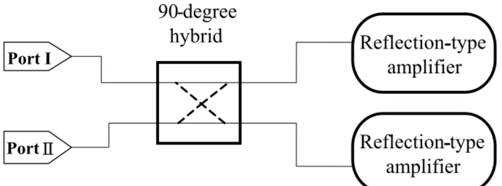
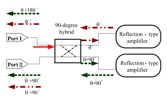
(28) Chapter 3 The Design of 5.8GHz BDA. coming from both ports, is proposed and demonstrated in this chapter. Fig. 3.1 shows the proposed configuration of the bi-directional amplifier, which contains two identical reflection-type amplifiers and a 3-dB quadrature hybrid [10]. The quadrature hybrid circuit can separate the input signal into two output signals with the phase difference of 90 degree and the same power level, and eliminate the signal at isolation port. The reflection-type amplifier, the device of only one end as the input and output ports, can amplify and reflect the incident signal. Port I and port II are the input and output of the bi-directional amplifier. In accordance with the principles of this circuit above, two signals produced by the quadrature hybrid circuit will be amplified by the reflection-type amplifiers and flash back to the hybrid circuit. Let a wave be incident on the bi-directional amplifier from port I as shown in Fig. 3.2, the signals with the same power and out of phase resulted at port I will cancel and the signals with the same power and the same phase resulted at port II will add. The Port I and Port II is the input and output ports of this amplifier. The role of two ports can be exchanged due to its bi-directional amplified capability. This designed process must pay attention to the oscillation condition of this circuit because its principles are similar to them of an oscillator.. 90-degree hybrid Port Ι. Reflection-type amplifier. PortⅡ. Reflection-type amplifier. Fig. 3.1 Configuration of the proposed bi-directional amplifier. 16.
(29) Chapter 3 The Design of 5.8GHz BDA. θ +180。 θ。. θ。. 90-degree hybrid. Port Ι θ。 θ+90。. PortⅡ θ +90。. Reflection - type amplifier. Reflection - type amplifier. θ+90。. θ +90。 Fig. 3.2 The principle of the bi-directional amplifier. 3.2 Circuit Design of the Bi-Directional Amplifier 3.2.1 Quadrature Hybrid As shown in Fig. 3.3, the quadrature hybrid must be realized by means of transmission lines with the quarter wavelength. The length is about 8mm at the operating frequency of 5.8GHz. The transmission line is not suitable for integrated circuit implementation.. Fig. 3.3 Circuit diagram of the conventional quadrature hybrid. 17.
(30) Chapter 3 The Design of 5.8GHz BDA. It is completed by adopting lump devices as shown in Fig 3.4 [11]. The symmetry of this circuit is important so that the inductors L1~L4 are using symmetric inductors provided by the standard CMOS process. Due to the lower Quality factor of the inductor implemented in integrated circuit implementation, the quadrature hybrid exhibits a through loss (S31) of 2 dB and a coupling loss (S41) of 2dB. The return loss and isolation, characterized by |S11| and |S21|, is better than 15dB as shown in Fig. 3.5(a). The phase difference between S31 and S41 is about 88∘ as shown in Fig. 3.5 (b).. Port 1. Port 2. L1 L2. L2 L1. Port 4. Port 3. C1. Fig. 3.4 The lumped quadrature hybrid. S-parameter (dB). 0. -10. S11 S21 S31 S41. -20. -30 4. 5. 6. 7. Frequency(GHz). Fig. 3.5(a) The S parameters of the quadrature hybrid 18.
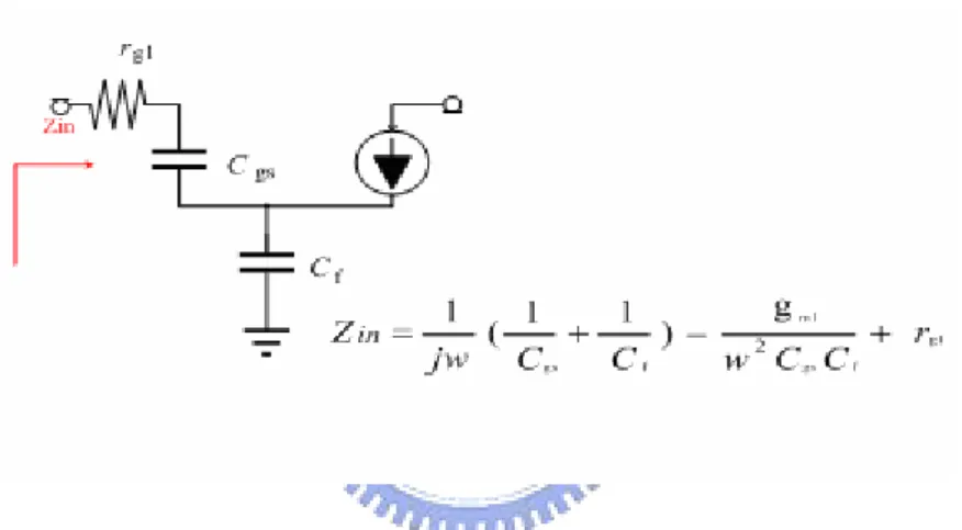
(31) Chapter 3 The Design of 5.8GHz BDA. phase difference (Degree). 200. 100. 0. S21 & S31 phase difference -100. -200 4. 5. 6. 7. Frequency (GHz). Fig. 3.5(b) The phase difference between S31 and S41. 3.2.2 Reflection-type Amplifier The incident signal can be reflected and amplified by the reflection-type amplifier. It means that the reflection coefficient Γ must be greater than one. The reflection coefficient Γ at the input port of the reflection-type amplifier is expressed as. Γ=. Z L − ZO Z L + ZO. (3.1). where ZL is the input impedance of the reflection-type amplifier and Z0 is the output impedance of the quadrature hybrid. From equation (3.1), the reflection coefficient Γ will be greater than one when the input impedance ZL is negative [12]-[13]. The reflection-type amplifier is designed as shown in Fig. 3.6. And Fig. 3.7 illustrates small-signal circuit of the reflection-type amplifier. The input resistance Zin can be derived as Zin =. g 1 1 1 ( + ) − 2 m1 + rg1 jw C gs C f w C gs C f. From (3.2), the negative resistance −. (3.2). g m1 can decrease by increasing gm1 or w C gs C f 2. decreasing Cf. The rg1 , resulted from MOS poly-gate, can be ignored due to multi-finger. Fig. 3.8 illustrates the simulation of input resistance. 19.
(32) Chapter 3 The Design of 5.8GHz BDA. Zin. Cf. Fig. 3.6 Schematic of the reflection-type amplifier. Fig. 3.7 Small-signal equivalent circuit model of reflection-type amplifier. 0. input resistance(Ohm). -10. -20. -30. Real(Z(1,1)) Image(Z(1,1)). -40. -50. -60 4.0. 4.5. 5.0. 5.5. 6.0. 6.5. 7.0. 7.5. Frequency (GHz). Fig. 3.8 The input resistance of reflection amplipier. 20.
(33) Chapter 3 The Design of 5.8GHz BDA. 3.2.3 Noise Discussion Fig. 3.10 shows the noise figure at operating frequency if the negative resistance shown in Fig 3.9 is ideal. The noise figure in Fig. 3.10 is caused by the loss of quadrature hybrid. However, there is no ideal negative resistance in practice. The negative resistance is designed as shown in Fig. 3.11. The noise figure and gain is depended on channel width. Fig. 3.12 illustrates the bi-directional amplifier noise figure increased when the channel width increase gradually. Fig. 3.13 illustrates the bi-directional amplifier gain increased when the channel width increase gradually. It means that the noise figure and gain in this design must be trade off. In order to improve the radiating filed, the focus of this design is the gain of the bi-directional amplifier.. Fig. 3.9 Bi-directional Amplifier with ideal negative resistance. 10. With ideal negative resistance. 9 8 7. NF(dB). 6 5 4 3 2 1 0 4.0. 4.5. 5.0. 5.5. 6.0. 6.5. 7.0. 7.5. Frequency (GHz). Fig. 3.10 The noise figure of bi-directional amplifier with ideal negative resistance 21.
(34) Chapter 3 The Design of 5.8GHz BDA. Fig. 3.11 Bi-directional Amplifier with negative resistance. n=1 n=21 n=31 n=41 n=51 n=64. 10 9 8 7. NF(dB). 6 5 4 3 2 1 0 4.0. 4.5. 5.0. 5.5. 6.0. 6.5. 7.0. 7.5. Frequency (GHz). Fig. 3.12 The noise figure increase as the width increase. n=1 n=21 n=31 n=41 n=51 n=64. 20. 15. Gain(dB). 10. 5. 0. -5. -10 4. 5. 6. 7. Frequency (GHz). Fig. 3.13 The gain increase as the width increase 22.
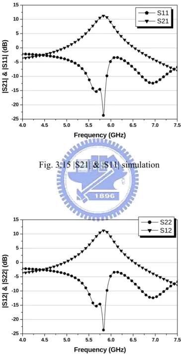
(35) Chapter 3 The Design of 5.8GHz BDA. 3.2.4 Bi-directional Amplifier According to above analysis, Fig. 3.14 shows the proposed bi-directional amplifier, which is composed of a quadrature hybrid, two identical reflection-type amplifiers and current source for reflection-type amplifiers.. Fig. 3.14 Schematic of the proposed Bi-directional Amplifier. 3.3 Simulated and Measured Results In this section, we show the simulation performance and measurement results of the bi-directional amplifier. For the poor experience in the beginning, the result is bad. Then we find the reason that the result is bad and improve on the layout.. 3.3.1 Simulation Performance Fig. 3.15 shows the magnitude of S11 and S21. Fig. 3.16 shows the magnitude of S12 and S22. The characteristic of the bi-directional amplifier was verified from Fig.. 23.
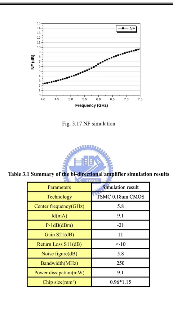
(36) Chapter 3 The Design of 5.8GHz BDA. 3.15 and Fig. 3.16. Fig. 3.17 shows the noise figure of the bi-directional amplifier. Table 3.1 summarizes the bi-directional amplifier performance of simulated results.. 15. S11 S21. 10. |S21| & |S11| (dB). 5 0 -5 -10 -15 -20 -25 4.0. 4.5. 5.0. 5.5. 6.0. 6.5. 7.0. 7.5. Frequency (GHz). Fig. 3.15 |S21| & |S11| simulation. 15. S22 S12. 10. |S12| & |S22| (dB). 5 0 -5 -10 -15 -20 -25 4.0. 4.5. 5.0. 5.5. 6.0. 6.5. 7.0. Frequency (GHz). Fig. 3.16 |S12| & |S22| simulation. 24. 7.5.
(37) NF (dB). Chapter 3 The Design of 5.8GHz BDA. 15 14 13 12 11 10 9 8 7 6 5 4 3 2 1 0. NF. 4.0. 4.5. 5.0. 5.5. 6.0. 6.5. 7.0. 7.5. Frequency (GHz). Fig. 3.17 NF simulation. Table 3.1 Summary of the bi-directional amplifier simulation results Parameters. Simulation result. Technology. TSMC 0.18um CMOS. Center frequency(GHz). 5.8. Id(mA). 9.1. P-1dB(dBm). -21. Gain S21(dB). 11. Return Loss S11(dB). <-10. Noise figure(dB). 5.8. Bandwidth(MHz). 250. Power dissipation(mW). 9.1. Chip size(mm2). 0.96*1.15. 25.
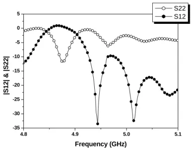
(38) Chapter 3 The Design of 5.8GHz BDA. 3.3.2 Measured results Fig. 3.18 shows the layout of the proposed bi-directional amplifier. The size of the layout is 1.13mm by 1.05mm including pads. The measurements were performed with the chip AC probe and DC bond-wire. Fig. 3.19 and Fig. 3.20 show the measured results of the bi-directional amplifier.. Fig. 3.18 Layout of the proposed bi-directional amplifier. S21 S11. 5 0. |S11| & |S21| (dB). -5 -10 -15 -20 -25 -30 -35 4.8. 4.9. 5.0. Frequency (GHz). Fig. 3.19 |S21| and |S11| measurements 26. 5.1.
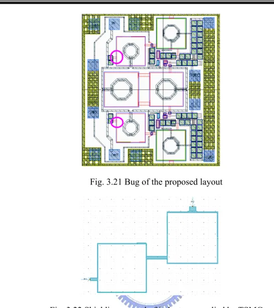
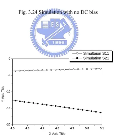
(39) Chapter 3 The Design of 5.8GHz BDA. S22 S12. 5 0. |S12| & |S22|. -5 -10 -15 -20 -25 -30 -35 4.8. 4.9. 5.0. 5.1. Frequency (GHz). Fig. 3.20 |S12| and |S22| measurements. 3.3.3 The reason for bad measured performance Experience teaches it. The grounding effect is important in the IC environment in spite of the short line. The quadrature hybrid consists of four grounding capacitances. In the layout the four capacitances didn’t connect to ground but to connect to shielding ground of the inductors as shown in Fig. 3.21. The shielding ground of the inductor is excessively narrow. Considering the shielding ground effect, we flatten the model of the inductors provided by the standard CMOS process and take the thin lines as shown in Fig. 3.22. Then we run EM simulation by ADS Momentum and obtain the layout effect model. Because of the effect caused by the shielding ground, the measurement with no DC bias was shown in Fig. 3.23. Fig. 3.24 shows the simulation with no DC bias. Fig. 3.25 shows the simulation with the shielding ground effect and no DC bias. Fig. 3.26 and Fig. 3.27 show the bi-directional amplifier simulation results with the shielding ground effect. We can verify that the bad results due to the shielding ground from above pictures. 27.
(40) Chapter 3 The Design of 5.8GHz BDA. Fig. 3.21 Bug of the proposed layout. Fig. 3.22 Shielding ground of inductors supplied by TSMC. Measurement S11 Measurement S21. 0 -2. |S11| & |S21| (dB). -4 -6 -8 -10 -12 -14 -16 -18 4.5. 4.6. 4.7. 4.8. 4.9. 5.0. 5.1. Frequency (GHz). Fig. 3.23 Measurement with no DC bias. 28.
(41) Chapter 3 The Design of 5.8GHz BDA. 0. S11 S21. |S21| & |S11| (dB). -2 -4 -6 -8 -10 -12 -14 4.6. 4.8. 5.0. 5.2. 5.4. 5.6. 5.8. 6.0. Frequency (GHz). Fig. 3.24 Simulation with no DC bias. Simultaion S11 Simulation S21. 0. Y Axis Title. -5. -10. -15. -20 4.5. 4.6. 4.7. 4.8. 4.9. 5.0. 5.1. X Axis Title. Fig. 3.25 Simulation with shielding ground effect and no DC bias. 29.
(42) Chapter 3 The Design of 5.8GHz BDA. S11 S21. 5 0. |S21| & |S11| (dB). -5 -10 -15 -20 -25 -30 -35 -40 -45 4.6. 4.8. 5.0. 5.2. 5.4. 5.6. 5.8. 6.0. Frequency (GHz). Fig. 3.26 Simulation with shielding ground effect S12 S22. 5 0. |S12| & |S22| (dB). -5 -10 -15 -20 -25 -30 -35 -40 4.6. 4.8. 5.0. 5.2. 5.4. 5.6. 5.8. 6.0. Frequency (GHz). Fig. 3.27 Simulation with shielding ground effect. 3.3.4 Improvement Fig. 3.28 shows the layout of the proposed bi-directional amplifier. The size of the layout is 1.15mm by 0.96mm including pads. Considering the layout effect, we take the long layout line as shown in Fig. 3.29 and run EM simulation by ADS Momentum so as to obtain the layout effect model. The improved chip will be back in August.. 30.
(43) Chapter 3 The Design of 5.8GHz BDA. Fig. 3.28 Layout of the improved bi-directional amplifier. Fig. 3.29 EM consideration. 3.4 Comparison and Summary The comparison of the proposed bi-directional amplifier against recently reported on amplifiers with bi-direction characteristic is shown in Table 3.2. It needn’t any switch to change the amplifier direction and needn’t control voltage to change the amplifier direction.. 31.
(44) Chapter 3 The Design of 5.8GHz BDA. Table 3.2 Summary of the comparison Ref.. Freq-Range (GHz). Gain S21 (dB). Return Loss (dB). switch. Voltage Control Direction. Size (mm2). Yes. NO. N/A. Yes. NO. 7.6*8.3. 42. 6. 10. 40. 10. 8. 2 ~ 18. 0 ~ 4.5. 12 ~ 30. 6 ~ 18. 0 ~ 12. 12 ~ 30. [16]. 8~12. 10. 10. NO. Yes. 5. [10]. 6. 9. 6. NO. NO. Off-chip. This work. 5.8. 11. 15. NO. NO. 1.15*0.96. [14] [15]. This section presents the amplifier provided with two directions by consisting of a quadrature hybrid and two reflection amplifier. The simulation result shows the achieved gain of 11 dB at 5.8GHz while the bi-directional amplifier draws 9.1mA. The size of the layout is 0.96mm by 1.15mm including pads.. 32.
(45) Chapter 4 The Design of Quadrature Hybrid. Chapter 4 The Design of A Miniaturized Quadrature Hybrid Using CMOS Active Inductors. Quadrature hybrid has been widely used in microwave systems for decades. Typically, quadrature hybrids are useful as power dividers or power combiners in various microwave circuits such as balanced amplifiers, balanced mixers, and phase shifters. Up to now, quadrature hybrids were implemented using the microstrip [17], stripline [18], finite-ground coplanar waveguide (CPW) [19], multilayer structures [20], and low-temperature co-fired ceramic (LTCC) [21]. Their sizes are relatively large due to the use of quarter-wavelength transmission lines, however the quarter-wavelength transmission line length has long impeded its applications in monolithic microwave integrated circuits (MMICs), especially for frequencies below 10 GHz. The ways to reduce the size of transmission lines such as using the folded lines configuration, capacitive loading, lumped element components, or the T or π equivalent-circuit model were employed to miniaturize quadrature hybrid [14]. 33.
(46) Chapter 4 The Design of Quadrature Hybrid. Though a smaller circuit size can be achieved, it suffers from higher insertion loss due to the lower quality factor (Q) in monolithic microwave integrated circuits. In this chapter, a lumped quadrature hybrid with active inductors is proposed to overcome the limitations of the on-chip passive components. The contents of this chapter below will introduce the complete framework of this quadrature hybrid using a 0.18 um CMOS process in detail and discuss the principles and considerations of each section.. 4.1 Architecture of the Quadrature Hybrid As shown in Fig. 4.1, the quadrature hybrid must be realized by means of transmission lines with the quarter wavelength. In order to reduce the circuit size effectively, the concept of replacing the transmission line sections with lumped passive components has also been adopted. Equation (4.1) is the ABCD matrix of the transmission line as shown in Fig. 4.2. Equation (4.2) is the Z matrix of the T-network as shown in Fig. 4.3. From equation (4.1), (4.2) and (4.3), a transmission line section with a characteristic impedance Z0 and electrical length βd can be replaced by its lumped equivalent T-network if βd=90°.. ⎡ A B ⎤ ⎡ cos βd ⎢C D ⎥ = ⎢ jY 0 sin βd ⎣ ⎦ ⎣. ⎡ Z11 Z12 ⎤ ⎡ ZA + ZC ⎥=⎢ ⎢Z ⎣ 21 Z 22 ⎦ ⎣ ZC ⎡ ⎡ Z11 Z12 ⎤ ⎢ ⎢Z ⎥=⎢ Z 22 ⎦ ⎣ 21 ⎢ ⎣⎢. A C 1 C. 34. jZ 0 sin βd ⎤ cos βd ⎥⎦. (4.1). ⎤ ZB + ZC ⎥⎦. (4.2). AD − BC ⎤ ⎥ C ⎥ D ⎥ C ⎦⎥. (4.3). ZC.
(47) Chapter 4 The Design of Quadrature Hybrid. Fig. 4.1 Circuit diagram of the conventional quadrature hybrid. Fig. 4.2 Transmission line section. Fig. 4.3 Lumped T-network. Fig. 4.4 Lumped quadrature hybrid 35.
(48) Chapter 4 The Design of Quadrature Hybrid. Since shunt inductance is preferable for the implementation of active inductors, an electrical length of 3λ 4 is employed in the proposed circuit topology. By replacing the transmission line sections with the π-networks, the equivalent circuit of the lumped quadrature hybrid is illustrated in Fig. 4.4.. 4.2 Circuit Design of the Quadrature Hybrid 4.2.1 Passive Inductor Using the spiral inductor provided by the standard CMOS process is convenient for designer. However, it is bad to use due to the lower Quality factor (Q) of the inductor implemented in integrated circuit implementation. Fig. 4.5 shows the inductance value and lower Q-factor of spiral inductor using a 0.18 um CMOS process. It means that the higher insertion loss suffers from the higher parasitical resistance of the spiral inductor implemented in integrated circuit implementation than SMD component. Also, the die size of one inductor as shown in Fig. 4.6 is about 0.26*0.26 mm2, and it will be larger if the inductance value is increasing. In order to reduce the circuit size and improve the Q-factor, the active inductor will be used and discussed later.. Fig. 4.5 Simulation of the spiral inductor using a 0.18 um CMOS process 36.
(49) Chapter 4 The Design of Quadrature Hybrid. Fig. 4.6 The die size of an inductor is about 0.26*0.26 mm2. Fig. 4.7 Spiral inductor connect with negative resistance. Fig. 4.8 The diagram of active inductor. 4.2.2 Active Inductor There are two ways to increase the quality factor, which plays an important role in the insertion loss. One is using spiral inductor connecting with a negative resistance [22]; the other is using the active inductor [23]. The former used negative resistance to cancel the parasitic resistance of spiral inductor as shown in Fig. 4.7. Though the quality factor is improved, the die size is large. Active inductors have advantages of 37.
(50) Chapter 4 The Design of Quadrature Hybrid. superior quality factor and small die size. The basic principle of the active inductor is based on a well-known gyrator theory [24]. The input impedance in Fig. 4.8 can be expressed by using Kirchoff's law. 1 ⎞ ⎛ − Ix = −G m 2 ⎜ G m1V x × ⎟ sC ⎠ ⎝. (4.4). sC p Vx = = sL I x Gm1Gm 2. (4.5). Leq =. Cp Gm1Gm 2. (4.6). From equations (4.4)、(4.5)、(4.6),Gm1 and Gm2 are the transconductor of the amplifier and Cp is the parasitic capacitance of the amplifier. The basic active inductor based on a gyrator topology can be realized by using a single MOS transistor as the transconductance (G ) element, as shown in Fig. 4.9. m. Fig. 4.9 Schematic of the basic active inductor 38.
(51) Chapter 4 The Design of Quadrature Hybrid. Fig. 4.10 Small-signal model of the basic active inductor. The input impedance of this basic active inductor, the small signal model as shown in Fig. 4.10, can be expressed by using Kirchoff's law.. Vin + (Vin − Va ) × ( sCgs 2 + sCgd 1 + gm 2) + Vin × sCgs1 = Iin ro 2. Va × ( sCgd 2 +. Yin = sCgs1 +. 1 ) + (Va − Vin) × ( sCgs 2 + sCgd 1) + Va × gm1 = 0 ro1. 1 + ro 2. (4.7). (4.8). 1 + sCgs1 × gm1) ro1 1 sCgs 2 + sCgd1 + sCgd 2 + ro1. ( sCgs 2 + sCgd1 + gm2)( sCgd 2 +. (4.9) ≈ sCgs1 +. 1 + gm2 + ro 2. gm1gm2 1 sCgs 2 + ro1. (Q sCgdi << sCgsi ). 39.
(52) Chapter 4 The Design of Quadrature Hybrid. From equation (4.9), Zin is equivalent to the conductance Yin. For the real part and the imaginary part, Zin can be equivalent RLC network as shown in Fig. 4.11. Equation (4.10)、(4.11)、(4.12) 、(4.13), derived by equation (4.9), show the values of all components in Fig. 4.11.. Fig. 4.11 Equivalent RLC model of active inductor. L=. Cgs 2 gm1gm 2. (4.10). R=. 1 gm1gm2ro1. (4.11). Cp = Cgs1. Gp =. 1 + gm 2 ro 2. (4.12). (4.13). 4.2.3 Quadrature Hybrid There are many methods to improve quality-factor of active inductors. Gain boosting, here we choose as shown in Fig. 4.12 [25], have the advantages of lower resistance. Fig. 4.13 shows the inductance and quality-factor simulation of this active inductor. The quality-factor of active inductor as shown in Fig. 4.13 is higher than spiral inductor. Also, the die size of one inductor as shown in Fig. 4.14 is about 40.
(53) Chapter 4 The Design of Quadrature Hybrid. 0.0851*0.070 mm2. The shunt inductances in the lumped equivalent circuit, as shown in Fig. 4.4, are replaced by the cascode active inductors. By employing the active inductors, the area can be reduction in this design. Fig. 4.15 shows the total circuit element. Also, another advantage of this design is the tunable frequency. The inductance is depended on the bias currents of transistors. The center frequency of the quadrature hybrid can be tunable by adjusting the bias current.. Fig. 4.12 Q-enhanced of cascode active inductor. 150. 2.0. L Q 1.5. 1.0. Q. L (nH). 100. 50 0.5. 0. 0.0 2. 4. 6. 8. 10. Frequency (GHz). Fig. 4.13 Simulation inductance of cascade active inductor 41.
(54) Chapter 4 The Design of Quadrature Hybrid. Fig. 4.14 The die size of an inductor is about 0.0851*0.070 mm2. Fig. 4.15 Complete schematic of quadrature hybrid with active inductors 42.
(55) Chapter 4 The Design of Quadrature Hybrid. 4.3 Simulation and Measurement Results In this section, we show the simulation performance and measurement results of this minimized quadrature hybrid. The chip layout and microphotograph of the proposed quadrature hybrid are shown in Fig. 4.16 and Fig. 4.17. The size of the layout is 0.74mm by 0.81mm including pads. The measurements were performed with the chip AC and DC probes.. Port1. Port4. Port2. Port3. Fig. 4.16 The chip layout of the proposed quadrature hybrid. Fig. 4.17 Microphotograph of the proposed quadrature hybrid. 43.
(56) Chapter 4 The Design of Quadrature Hybrid. Based on the corner-case SS, the compare of simulation performances and measurement results at 1.8V and 1.5V supply voltage was shown from Fig. 4.18 to Fig. 4.21. Fig. 4.18 shows the simulated and measured S11 and S21. The measurement S11 is under -10dB and S21 is about -4dB. Fig. 4.19 shows the simulated and measured S31 and S41. The measurement S41 is under -15dB and S31 is about -2dB.. 0. |S11| & |S21| (dB). -10. -20. Measurement Simulation. -30. -40 4. 5. 6. 7. Frequency (GHz). Fig. 4.18 Simulated and measured S11 and S21. 0. |S31| & |S41| (dB). -10. -20. Measurement Simulation -30. -40 4. 5. 6. 7. Frequency (GHz). Fig. 4.19 Simulated and measured S31 and S41 44.
(57) Chapter 4 The Design of Quadrature Hybrid. The phase difference between S21 and S31 is 94。~100。 as shown in Fig. 4.20. Another advantage of this design is the tuning range. Fig. 4.21 shows the tuning range of S11.. Phase Difference (Degree). 200. 100. 0. Measurement Simulation. -100. -200 4. 5. 6. 7. Frequency (GHz). Fig. 4.20 Simulated and measured phase difference between S21 and S31. 0. S11 (dB). -10. -20. S11 tuning range. -30. -40 4. 5. 6. Frequency (GHz). Fig. 4.21 S11 tuning range. 45. 7.
(58) Chapter 4 The Design of Quadrature Hybrid. Fig. 4.22 shows the tuning range of S21. The tuning range of S31 is shown in Fig. 4.23.. 0. S21 (dB). -10. -20. S21 tuning range. -30. -40 4. 5. 6. 7. Frequency (GHz). Fig. 4.22 S21 tuning range. 0. S31 (dB). -10. -20. S31 tuning range -30. -40 4. 5. 6. Frequency (GHz). Fig. 4.23 S31 tuning range. 46. 7.
(59) Chapter 4 The Design of Quadrature Hybrid. The tuning range of S41 is shown in Fig. 4.24. Fig. 4.25 shows the phase difference between S21 and S31. The tuning range of this design is from 5GHz to 6GHz. Table 5.1 is the summary of the quadrature hybrid simulation and measurement results.. 0. S41 (dB). -10. -20. -30. S41 tuning range -40 4. 5. 6. 7. Frequency (GHz). Fig. 4.24 S41 tuning range. Phase Difference (degree). 200. 100. 0. -100. Phase difference tuning range. -200 4. 5. 6. Frequency (GHz). Fig. 4.25 Phase difference tuning range. 47. 7.
(60) Chapter 4 The Design of Quadrature Hybrid. Table 4.1 Summary of simulation and measurement results Specification. Simulation results. Measurement results. Id(mA). 20.6. 21mA. Central frequency(GHz). 5.3. 5.4. Through loss (dB). 0.7. 1. Coupling loss (dB). 0.7. -1. Return Loss S11(dB). <-20. <-10. Isolation (dB). <-20. <-15. Phase difference. 90∘+ 2∘. 95∘ ~ 100∘. Bandwidth (MHz). 500. 280. Tuning Range (GHz). 5~6. 5~6. Power dissipation(mW). 37. 37.8. 0.33*0.5 / 0.732*0.8. NA / 0.8*0.9. Active Area/ Die Area (mm2). 4.4 Comparison and Summary The comparison of the proposed quadrature hybrid with active inductors against recently reported quadrature hybrid is shown in Table 4.2. It indicates that the proposed quadrature hybrid provides more compact chip size, good dissipated loss and tuning range. Table 4.2. Summary of the comparison. Ref.. Process. FreqRange (GHz). S11 (dB). S21 (dB). S31 (dB). S41 (dB). Phase difference. Tuning range (GHz). Active Area/ Die Area (mm2). [11]. Si substrate. 8.5. <-18. -4.6. -5.2. <-20. 90。. No. 0.6 * 0.6. [20]. GaAs. 18-27. <-15. -5.5+0.5. -5.5+0.5. <-15. N/A. No. 0.49 * 0.53. [21]. LTCC. 2.147-2.47. <-15. -4 ~ -5.1. -2.6~ -2.89. <-15. 93。 ~105。. No. 4.126 * 3.835. This work. 0.18um CMOS. 5.4. <-10. -4. -2. <-15. 95。 -100。. 5-6. 0.33*0.5 / 0.8*0.9. 48.
(61) Chapter 5 The Design of Mixer. Chapter 5 The Design of WiMAX Mixer with an Integrated Miniaturized Passive Balun. Balun is useful for conversion between differential and single-ended signal. The balance LNA usually involves double power consumption than single topology. Balun, transition the single-ended input signal to differential output signal, is necessary while the LNA is single topology. On-chip balun can reduce the size of off-chip balun. Passive baluns is preferred for the reduction of power consumption in wireless system than general active baluns. In this chapter, the miniaturized balun is applied in the integration of Gilbert Mixer and implemented on 0.18 um CMOS process.. 49.
(62) Chapter 5 The Design of Mixer. 5.1 Architecture of the proposed Mixer Fig. 5.1 shows the block diagram of the proposed Mixer. Connecting single-ended LNA and double-balance mixer, the on-chip balun is necessary. The passive loss of On-chip balun is higher than off-chip or active balun due to the worst quality-factor. The loss incurs noise penalty, however the signal incurs only a slight noise penalty because the passive loss occur after the LNA.. Fig. 5.1 The block diagram of the proposed Mixer. 5.2 Circuit design of the proposed Mixer 5.2.1 Balun Most balun structures utilize either distributed or lumped elements. Distributed baluns are composed of sections of λ/2 transmission line orλ/4 coupled line. These structures occupy large size especially in the integrated circuit implementation. As 。 lumped element balun is formed with low pass filter, 90 ahead, and high pass filter,. 90。 behind, it always exhibit poor balun balance across frequency [26]. Recently, balun structures consisted of both distributed and lumped elements have been proposed [27]. The balun as shown in Fig. 5.2 has been investigated in [28]. By adding two capacitors C2 and C3, the coupled lines length can be reduced and two poles induce because of the coupled resonators. C1 is the input matching. Fig. 5.3 shows the S-parameter. The phase difference is as shown in Fig. 5.4. Fig. 5.5 shows the die size of the proposed balun is about 0.26*0.26 mm2. 50.
數據
+7
相關文件
了⼀一個方案,用以尋找滿足 Calabi 方程的空 間,這些空間現在通稱為 Calabi-Yau 空間。.
Wang, Solving pseudomonotone variational inequalities and pseudocon- vex optimization problems using the projection neural network, IEEE Transactions on Neural Networks 17
volume suppressed mass: (TeV) 2 /M P ∼ 10 −4 eV → mm range can be experimentally tested for any number of extra dimensions - Light U(1) gauge bosons: no derivative couplings. =>
Define instead the imaginary.. potential, magnetic field, lattice…) Dirac-BdG Hamiltonian:. with small, and matrix
• Formation of massive primordial stars as origin of objects in the early universe. • Supernova explosions might be visible to the most
(Another example of close harmony is the four-bar unaccompanied vocal introduction to “Paperback Writer”, a somewhat later Beatles song.) Overall, Lennon’s and McCartney’s
專案執 行團隊
Microphone and 600 ohm line conduits shall be mechanically and electrically connected to receptacle boxes and electrically grounded to the audio system ground point.. Lines in
