國
立
交
通
大
學
顯示科技研究所
碩
士
論
文
量子點面射型雷射高頻特性之研究
High Speed Characteristics of Quantum Dot
Vertical Cavity Surface-Emitting Laser
研 究 生:蔡文凱
指導教授:郭浩中 教授
量子點面射型雷射高頻特性之研究
High Speed Characteristics of Quantum Dot Vertical Cavity
Surface-Emitting Laser
研 究 生:蔡文凱 Student:Wen-Kai Tsai
指導教授:郭浩中 Advisor:Hao-Chung Kuo
國 立 交 通 大 學
顯示科技研究所
碩
士 論 文
A ThesisSubmitted to Institute of Electronics College of Engineering National Chiao Tung University
in partial Fulfillment of the Requirements for the Degree of
Master in
Electo-Optical Engineering
July 2006
量子點面射型雷射高頻特性之研究
研究生:蔡文凱 指導教授:郭浩中教授
國立交通大學顯示科技研究所
摘要
本論文旨在研究量子點面射型雷射以及其動態特性的分析。論文分為三個部 分,第一個部分,我們提出從雷射的直流特性,包括 LIV 曲線、發光頻譜圖及其變 溫特性。此外也展示此量子點雷射的高頻特性,且展示了 2.5Gb/s 的眼圖。論文的 第二部分,則是利用外部注入鎖定( injection locking )的技術,來改善雷射的高 頻特性,包括增進雷射的小信號頻寬,從原本的 1.7GHz 提升到 7.2GHz,並且在 7GHz 的頻帶載入 50Mb/s 信號,可以觀測出一個清晰的眼圖。此外,利用注入鎖定技術, 可以改善雷射的諧波失真項的特性,從 100MHz~1.4GHz 都能改善 10dB 以上。論文的 最後,則是利用量子點面射型雷射來當作延遲光行進速度的元件,隨著偏壓電流的 不同,可以形成不同延遲的效果,在 10GHz 的操作之下,可以達到 42ps 的延遲,我 們同時也針對不同輸入信號強度以及不同頻率下的操作,來觀測其延遲的情形。High Speed Characteristics of Quantum Dot Vertical
Cavity Surface Emitting Laser
Student:Wen-Kai Tsai Advisor:Prof. Hao-Chung Kuo
Display Institute
National Chiao Tung University
Abstract
The thesis studies the fabrication, measurements and the high speed characteristics of quantum dots vertical cavity surface-emitting laser (QD VCSEL). This thesis can be divided into three parts. In the first parts, we present monolithic QD VCSELs operating in the 1.3 µm optical communication wavelength. The QD VCSELs have adapted fully doped structure on GaAs substrate. The output power is ~ 330 µW with slope efficiency of 0.18 W/A at room temperature. Single mode operation was obtained with side-mode suppression ratio of > 30 dB. Modulation bandwidth and eye diagram in 2.5 Gb/s was also presented. In the second part of this thesis, we report the dynamic characteristics of 1.3µm QD VCSEL without and with light injection. The 3 dB frequency response of QD VCSEL based on TO-Can package is enhanced from the free-running 1.75 GHz to 7.44 GHz with the light injection technique. We also report the second harmonic distortion of QD VCSEL with and without external light injection. We observed that the second harmonic distortion of the QD VCSEL with light injection has been suppressed by more than 14 dB. A 50 Mb/s non-return-to-zero (NRZ) pseudo-random binary sequence (PRBS) data with 231 – 1 pattern length from a pattern generator is mixed with a 7 GHz RF carrier and then used to directly modulate the QD VCSEL. The QD VCSEL without light injection cannot generate 7-GHz 50-Mb/s data due to the limited frequency response. With light injection technique, the corresponding eye diagrams can be clearly observed. At the end of this thesis, we experimentally demonstrate tunable slow light in an 1.3 µm QD VCSEL at 10 GHz. Tunable optical group delays are achieved by varying the bias
誌 謝
在這兩年的研究生涯中首先要感謝的是王興宗教授細心的指導與教誨,讓我學 習到實驗的技術與認真嚴謹研究的態度。此外,也感謝我的指導教授郭浩中教授, 有他的指導和提供專業的實務與經驗,在實驗研究方面給予我相當大的幫助。我也 要感謝盧廷昌老師的指導,他不時提醒我在研究成果上的缺失和寶貴的建議,讓我 受益良多。 研究的過程之中,特別要感謝張亞銜學長、彭朋群學長及曾國峰學長,在實驗 上給予我相當多的指導與幫助,讓我從一個門外漢進而能夠獨立來操作實驗,碩士 班兩年能夠順利畢業,絕對要感謝你們的栽培,謝謝學長們的指導。同時也要感謝 工研院的研究團隊,在雷射設計與製作方面的幫忙,此外,每個星期的會議討論, 也讓我吸取到不少寶貴的經驗。 在實驗室裡面,感謝同學游敏、意偵、皇伸、柏傑、志堯、宗鼎、剛帆陪我一 起走過這兩年的歲月。感謝博士班的學長姊們,道鴻學長、芳儀學姊、忻宏學長、 小強學長、小豬學長、宗憲學長、乃芳學姊、小賴學長在實驗和課業經驗上的分享。 也要感謝碩一的學弟妹,瑞農、孟儒、潤琪、立凡、家璞、卓奕、碩均、昀浦,在 實驗上的幫助與營造溫馨和諧的實驗室氣氛。也感謝助理麗君在實驗室行政方面的 協助。 最後,要特別感謝我親愛的父母親與家人對我全心全力的支持及無怨無悔的付 出,再我遭遇挫折的時候鼓勵我,讓我能順利完成學業。 2006/7/6 文凱Contents
Abstract (in Chinese)
Abstract (in English)
Acknowledgment
Contents
List of figures
Chapter 1
Introduction
1
1.1
Introduction
of
Quantum
Dot
VCSEL
1
1.2
Review
of
Injection
Locking
technique 1
1.3
Review
of
Slow
Light 2
1.4
Organization
of
the
Dissertation
3
Chapter 2
High speed modulation of Quantum
Dot
VCSEL 6
2.1
Sample
structure
and
Fabrication
process
6
2.2
DC
Characteristics
of
QD
VCSEL
8
2.2.1
Experimental
Setup
8
2.2.2
Results
and
Discussion
9
2.3
High
speed
modulation
of
QD
VCSEL
10
2.3.1 Theory
10
2.3.2
Experimental
Setup
13
2.3.3
Results
and
Discussion
14
2.4 Conclusion
15
Chapter 3
Injection
Locking
of
Quantum
Dot
VCSEL
22
3.1 Modulation Response Enhancement by injection locking
22
3.1.1 Theory
22
3.1.2
Experimental
Setup
26
3.1.3
Results
and
Discussion
26
3.2
Reduction of nonlinear distortion by injection locking technique27
3.2.1 Theory
28
i ii iii iv viChapter 4
Slow
Light
in
Quantum
Dot
VCSEL
39
4.1 Theory
39
4.2 Tunable Slow Light Device of Quantum Dot VCSEL
42
4.2.1
Experimental
Setup
42
4.2.2
Results
and
Discussion
43
4.3 Conclusion
43
Chapter 5
Summary
52
5.1 Summary
52
List of figures
Chapter 2
Fig. 2-1 QD VCSELs device structure. Inset is the top view image of the QD VCSEL. Fig. 2-2 Probe station measurement instrument setup
Fig. 2-3 L-I-V relationship of QD VCSEL. Inset is the near-filed pattern of the VCSELs
at 3mA
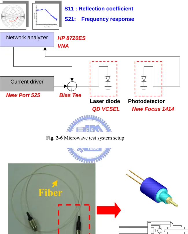
Fig. 2-4 Emission spectra of QD VCSEL at room temperature. Fig. 2-5 Temperature dependent L-I relationship of QD VCSEL. Fig. 2-6 Microwave test system setup
Fig. 2-7 The QD VCSEL TO-Can package and the single-mode fiber are assembled by
laser welding technique.
Fig. 2-8 Small signal modulation response of QD VCSEL
Fig. 2-9 3dB frequency as a function of square root of current above threshold current. Fig.2-10 Eye diagram of the QD VCSELs at (a) 1.25 Gb/s and (b) 2.5 Gb/s ( The time
scale was 200 ps/div and 100 ps/div)
Chapter 3
Fig. 3-1 (a) Schematic diagram of the quantum dot vertical cavity surface emitting laser
(b) Experimental setup for the injection locking of QD VCSEL (DFB: DFB laser, VA: variable optical attenuator, OC: optical circulator, OSA: optical spectrum analyzer, PC: polarization controller, PD: photodetector, Amp: electrical amplifier)
Fig. 3-2 Small-signal frequency response of QD VCSEL at different bias currents. Fig. 3-3 Small-signal frequency response of QD VCSEL at different injection powers. Fig. 3-4 3 dB frequency response as a function of injection power.
Fig. 3-5 Experimental setup for the quantum dot VCSEL without and with light
injection in a subcarrier multiplexed system. (PG: pattern generator, LPF: low pass filter, RFA: RF amplifier, PD: photodetector)
Fig. 3-6 7-GHz 50-Mb/s data signal at point A (a) without light injection (b) with light
injection.
Fig. 3-7 Received eye diagrams of 50-Mb/s signal.
Fig. 3-8 Experimental setup for measuring the third-order intermodulation
distortion (IMD3) of quantum dot VCSEL without and with light injection.
Fig. 3-9(a) Electrical spectrum of QD VCSEL without external light injection
(b) Electrical spectrum of QD VCSEL with external light injection
(c) Second harmonic distortion as a function of modulation frequency for the QD VCSEL with and without external light injection.
Fig.4-2. Experimental setup for measuring the optical group delays in QD VCSEL. (Mod:
electro-optic modulator, VA: variable optical attenuator, C: optical circulator, OC: optical coupler, PC: polarization controller, RFA: RF amplifier, PD: photodetector, OSA: optical spectrum analyzer)
Fig.4-3. The measurements of time delay for a 10 GHz probe signal at the various bias
currents of QD VCSEL.
Fig.4-4. Absorption dip of QD VCSEL
Fig.4-5. Optical spectrum of tunable laser injecting into QD VCSEL
Fig.4-6. The waveform at different modulation frequencies of probe signals.
Fig.4-7. The relationship between the time delays and modulation frequencies of probe
signals.
Fig.4-8. The waveform at different powers of probe signals.
Fig.4-9. The time delays as a function of bias currents of QD VCSEL and optical power
Chapter 1 Introduction
1.1 Introduction of Quantum Dot VCSEL
Vertical-cavity surface-emitting lasers (VCSELs) at around 1.3 µm fabricated on GaAs substrates have been expected to realize high-performance and low-cost light sources for fiber-optic communication systems. The large conduction band offset improves the temperature performance over that of conventional InP-based materials. The GaAs system provides high-performance AlGaAs/GaAs DBR mirrors and permits the use of the well-established oxide-confined GaAs-based VCSEL manufacturing infrastructure. So far, the most promising materials at 1.3 µm on GaAs substrate were GaInAsN quantum wells (QWs) [1-3] and quantum dots (QDs) [4-6]. Each of these solutions offers some advantages over its counterpart, but further extend the emission wavelength is relatively easy in quantum dots than GaInAsN. QDs edge-emitting lasers have also been proven to exhibit excellent performance characteristics, including low threshold current, temperature insensitive threshold current, and high differential gain. For VCSELs, QDs [7] are particularly advantageous, as nonequilibrium carriers are localized in the QDs and thus spreading of nonequilibrium carriers out of the injection region can be suppressed. This may result in ultralow threshold currents at ultrasmall apertures [7-8].ġ
1.2 Review of Injection Locking technique
Since the early 1980s, the research topic injection locking of semiconductor lasers has attracted much interest. Its applications include receiver end design in optical coherent communication[9], laser spectral narrowing[10], suppression of laser noise[11], the reduction of frequency chirp under modulation[12], and improving the laser intrinsic frequency response[13].
For digital communication, the high-linewidth enhancement factor leads to high chirp that is undesirable. In analog fiber-optic transmission systems have many applications such as CATV and fiber radio systems. [14] In these applications, the direct modulation of semiconductor lasers can be used for transmitting subcarrier-multiplexed signals at
frequency, the nonlinearity resulting from the coupling between photons and electrons in the laser cavity is dominant. This coupling also results in the relaxation oscillation resonance. Such distortions can cause severe system performance degradation, because they cause inter-channel interference that limits the number of channels as well as transmission distance. For the highest capacity systems, designers typically have chosen to incorporate an external modulation device to a continuous-wave laser. Though this may achieve the desired performance requirements, it does so with the cost of additional system complexity. If possible, a directly modulated laser with higher performance would be ideal. Injection Locking can increase the laser relaxation oscillation frequency, which causes the intrinsic nonlinear distortion suppression in directly modulated semiconductor lasers and gives us the additional design freedom with greatly increased performance that makes injection-locked directly modulated lasers a viable candidate for future analog and digital networks.
1.3 Review of Slow Light
In optical communication, a controllable variable optical buffer is one of the most critical components. In such buffer, optical data would be kept in optical format throughout the storage time without being converted into electronic format. The turn-on and turn-off time should be variable with an external control. The most important application of optical buffers is perhaps all-optical routers in packet-switched networks. A router is used in networks to interconnect end-user systems to each other where packets are the basic units of information that are transported. A router often connects many networks and performs decisions on how to send packets from its source to its destination in the network. Packet switching is a method of communication whereby information is broken up into blocks of limited length called packets. They are then switched in a network by routers. The key building blocks of an electronic router include a switch fabric, processors, and buffers. The key missing component for an all-optical router is an all-optical buffer. With optical buffers, one packet can be stored in the buffer temporarily, allowing the other packet to go first. Until the traffic is cleared at the output port, the packet stored in the buffer is released. An all-optical router can potentially alleviate the traffic congestion in future very-high-bandwidth networks. However, variable optical delay lines (also called “slow light” devices) and buffers will be crucial components in
optical communication, phased array antenna, and signal processing systems. There are several technical approaches to implement an optical buffer. No matter what methods, the medium which the optical signal travels in should be varied by either increasing the path length or reducing the signal group velocity. The former can be achieved by using of a fiber delay line or resonant cavity and the latter has several possibilities, such as EIT, CPO. Recently, tunable slow light using an InGaAsP quantum well Fabry-Perot laser has been reported [15]. Tunable optical group delays 14 ps for 2 GHz sinusoidal signal have been demonstrated, and the delay-bandwidth product was 0.028. Moreover, tunable slow light using a quantum well VCSEL fabricated on InP-based materials also has been proposed [16]. The modulation frequency of probe signal between 1-3 GHz was presented, and the delay-bandwidth product was 0.28 (100 ps × 2.8 GHz).
1.4 Organization of the thesis
This thesis consists of three related parts. In Chapter 2, we demonstrate monolithically single-mode QD VCSELs with high side-mode suppression ratio (> 30 dB) and report the temperature performance and dynamic properties including bandwidth and eye diagram.
In Chapter 3, we report the experimental characterization of 1.3µm QD VCSEL
with and without external light injection. Significant frequency response enhancement has been observed. Furthermore, we demonstrate that this frequency response enhancement allows us to improve the performance of subcarrier multiplexed (SCM) system. We also report the third-order intermodulation distortion (IMD3) of QD VCSEL with and without external light injection.
In Chapter 4, we report the slow light in the monolithically single-mode QD VCSEL. Tunable optical group delay can be achieved by adjusting the bias current. A 10 GHz modulation signal with tunable optical group delays 42 ps has been demonstrated. We
Reference
[1] N. Tansu and L. J. Mawst, "Temperature sensitivity of 1300-nm InGaAsN quantum-well lasers", IEEE Photonics Technology Letters, vol. 14, no. 8, pp. 1052-1054, 2002.
[2] C. W. Tu and Pkl Yu, “Material properties of III-V semiconductors for lasers and detectors,” MRS Bulletin, vol. 28, pp. 345-349, 2003.
[3] M. Kawaguchi, T. Miyamoto, E. Gouardes, D. Schlenker, T. Kondo, F. Koyama and K. Iga “Lasing Characteristics of Low-Threshold GaInNAs Lasers Grown by Metalorganic Chemical Vapor Deposition,”Japanese Journal of Applied Physics, vol. 40, pp. L744–L746, 2001.
[4] S. L. Chuang, N. Holonyak, Jr. “Quantum-well assisted tunneling injection quantum-dot lasers,” Conference on Lasers and Electro-Optics, Technical Digest, vol. 1, pp. 297, 2002.
[5] T. Yang, J. Tatebayashi, S. Tsukamoto and Y. Arakawa,” Highly uniform self-assembled InAs/GaAs quantum dots emitting at 1.3µm by metalorganic chemical vapor deposition,” Physica E, vol. 26, pp. 77-80, 2005.
[6] N. N. Ledentsov, "Long-wavelength quantum-dot lasers on GaAs substrates: from media to device concepts," IEEE Journal of Selected Topics in Quantum Electronics, vol. 8, pp. 1015 - 1024, 2002.
[7] N. N. Ledentsov, M. Grundmann, F. Heinrichsdor, D. Bimberg, V.M. Ustinov, A. E. Zhukov, M. V. Maximov, Zh. I. Alferov, J. A. Lott, “Quantum-Dot Heterostructure Lasers,” IEEE Journal of Selected Topics in Quantum Electronics, vol. 6, no. 3, pp. 439-451, 2000.
[8] J. A. Lott, N. N. Ledentsov, V. M. Ustinov, A. Yu. Egorov, A. E. Zhukov, P. S. Kop’ev, Zh. I. Alferov, and D. Bimberg, “Vertical cavity lasers based on vertically coupled quantum dots,” Electronics Letters, vol. 33, pp. 1150-1151, 1997.
[9] Y. Yamamoto and T. Kimura, “Coherent optical fiber transmission systems,”IEEE J.
Quantum Electron., vol. QE-17, pp. 919–935, June 1981.
[10] P. Gallion, H. Nakajima, G. Debarge, and C. Chabran, “Contribution ofspontaneous emission to the linewidth of an injection-locked semiconductorlaser,” Electron. Lett., vol. 22, pp. 626–628, 1985.
[11] K. Iwashita and K. Nakagawa, “Suppression of mode partition noise by laser diode light injection,” IEEE J. Quantum Electron., vol. QE-18, pp.1669–1674, Oct. 1982. [12] N. A. Olsson, H. Temkin, R. A. Logan, L. F. Johnson, G. J. Dolan, J.P. Van der Ziel,
and J. C. Campbell, “Chirp-free transmission over 82.5km of single mode fibers at 2 Gbit/s with injection locked DFB semiconductor lasers,” IEEE J. Lightwave Technol., vol. LT-3, pp. 63–67, Feb.1985.
[13] X. Meng, T. Chau, and M. C.Wu, “Experimental demonstration of modulation bandwidth enhancement in distributed feedback lasers with external light injection,”
Electron. Lett., vol. 34, no. 21, pp. 2031–2032, 1998.
[15] S. Minin, M. R. Fisher, S. L. Chuang, "Current-controlled group delay using a semiconductor Fabry-Perot amplifier," Applied Physics Letters, vol. 84, pp. 3238-3240, 2004.
[16] X. Zhao, P. Palinginis, B. Pesala, C. J. Chang-Hasnain, P. Hemmer, "Tunable ultraslow light in vertical-cavity surface-emitting laser amplifier," Optics Express, vol. 13, pp. 7899-7904, 2005.
Chapter 2 High speed modulation of Quantum Dot VCSEL
In this chapter, we present monolithic quantum-dot vertical-cavity surface-emitting laser (QD VCSELs) operating in the 1.3 µm optical communication wavelength. The QD VCSELs have adapted fully doped structure on GaAs substrate. The output power is ~ 330 µW with slope efficiency of 0.18 W/A at room temperature. Single mode operation was obtained with side-mode suppression ratio of > 30 dB. Modulation bandwidth and eye diagram in 2.5 Gb/s was also presented.
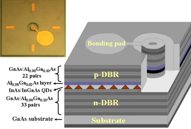
2.1 Sample structure and Fabrication process
All structures were grown on GaAs (100) substrates by molecular beam epitaxy (MBE). The epitaxial structure was as follows (from bottom to top) - n+-GaAs buffer, 33.5-pair n+-Al0.9Ga0.1As/n+-GaAs (Si-doped) distributed Bragg reflector (DBR),
undoped active region, p-Al0.98Ga0.02As oxidation layer, 22-pair
p+-Al0.9Ga0.1As/p+-GaAs DBR (carbon-doped) and p+-GaAs (carbon-doped) contact
layer. The graded-index separate confinement heterostructure (GRINSCH) active region consisted mainly of three stack of QDs active region, with PL emission at 1.266 µm, embedded between two linear-graded AlxGa1-xAs (x = 0 to 0.9 and x = 0.9 to 0) confinement layers. The thickness of the cavity active region was 1λ. Carbon was used as the p-type dopant in the DBR to increase the carrier concentration (2-3×1018 cm-3). The interfaces of both the p-type and n-type Al0.9Ga0.1As/GaAs DBR layers are linearly
graded to reduce the series resistance. The optical characteristics of QDs were optimized through PL measurement and structural analysis. The details of the process were fully described in our previous works [1]. The mesa diameter of the fabricated device is 26µm with a 5 µm oxide aperture, and the device surface is quasi-planar so that the annular p-contact metal and the bond pad are on the same level. The device structure is shown in Fig.2-1. The p-contact was formed by directly depositing Ti/Pt/Au on the upper heavily doped p+ GaAs contact layer, and Au/Ge/Ni/Au was deposited on the bottom side of the substrate after it had been thinned down, and the shaded region beneath the bond pad represents the implanted region. It is worth noting that neither the intra-cavity /
co-planar metal contact nor polyimide resin planarization been used in the process. After metal annealing, the sample was immediately probe tested on the wafer level to extract the static operation characteristics, and was subsequently divided into two pieces. One piece was diced for packaging later, and the other was sent to be subjected to H+ implantation with a dose of 1015cm-2 for the purpose of further reducing the parasitic capacitance. Preliminarily we adopt four different proton energies in the range from 300 to 420keV according to the stopping and range of ions in matter (SRIM) simulation results, but the ideal combination of proton implantation energies in relative experiments currently we finished has not been optimized yet. The proton energy we used in this experiment was stronger than that used for conventional proton-implanted VCSELs. The reason for using such high-energy protons to bombard the sample is simply that the surface of the implanted region has already been passivated by the presence of 1500-Å-thick SiO2 and 4000-Å-thick metal bond pad. When a charged particle such as H+ penetrates a dielectric material such as SiO2, it is subjected to scattering because of the built-in electric field result from the dipole and metal-insulator-semiconductor interfaces. However the incident proton has seldom been influenced by the thicker metal bond pad because there is no electric field inside the metal. Hence, we need a higher energy to make sure the implanted proton can penetrate the SiO2 and eventually locate at the right depth, that is, as close as possible to the active region. The implantation region was kept apart the mesa to prevent the damage which was caused by ion bombardment from destroying the active region.
2.2 DC Characteristics of QD VCSEL
2.2.1 Experimental Setup
In order to precisely measure characteristics of QD VCSEL, such as LIV curve, optical spectrum, or near field pattern, we need to setup a system which can test our sample on wafer level or packaged level. Probe station was a basic instrument to meet our needs. Scheme of probe station system, illustrated in Figure 2-2, include probe station, current source, and power-meter module. Keithley 238 can provide precisely continuous current with laser diode and measure relative voltage synchronously. Newport power meter module (model 1835C) with photodiode and power meter can measure the light output power of the laser diode. An integration sphere was used to pick up whole emitting power from VCSEL to improve the accuracy of power measurement.
The VCSEL device was placed on a platform of the probe station and was injected bias current with microprobe. Threshold condition, slope efficiency, turn-on voltage and differential resistance can be obtained from L-I-V information by sweeping bias current. Near-field pattern was obtained by specific CCD. Emission spectrum of the device was measured by optical spectrum analyzer (OSA, Advantest 8381). A multi-mode fiber probe was placed close to the emission aperture to take optical spectra. The OSA had spectrum resolution of 0.1nm which was adequate to measure VCSEL lasing spectra.
2.2.2 Results and Discussion
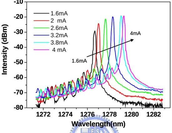
Fig. 2-3 plots curves of light output and voltage versus current (LIV). The threshold current is ~ 1.8 mA and the threshold current density is 7.6 kA/cm2. The output power rollover occurs as the current increases above 4mA with maximum optical output of 0.33mW at 20°C. In addition, the VCSEL is single polarization in the full operating range with ratio of ~20dB. Inset of Fig 2-3 is the near-filed pattern of the QD VCSEL biased at 3mA which indicated the fundamental mode lasing. Fig 2-4 shows the typical emission spectra of the quantum-dot VCSELs, which indicate single transverse mode operation in the whole operation range with a lasing wavelength of ~1.278 µm and side mode suppression ratio (SMSR) > 30dB.
To investigate the temperature dependence of the QD VCSEL, LI curves were measured from room temperature to 55oC with current step of 0.01 mA, as shown in Fig. 2-5. The threshold current varies only 0.15 mA (< 10% of Ith ) with temperatures from
10°C to 45°C and the slope efficiency drops from 0.18 to 0.1 W/A. The small temperature dependence of threshold current corresponds to a characteristic temperature (T0) of 450K, a high value comparing with the InGaAs(N) VCSEL in 1.3 µm. The high
characteristic temperature was attributed to the wide gain spectra of the quantum dots gain media. When temperature increases, the wide gain spectra make the alignment between gain spectra and cavity resonance not sensitive, and therefore improve the T0.
However, increase of threshold current with temperature and the quench of output power were also observed after 50oC which implies the gain of the quantum dots decreases severely in higher temperature.
2.3 High speed modulation of QD VCSEL
2.3.1 Theory:Small signal modulation
Under small signal modulation, the carrier and photon density rate equation are used to calculate relaxation resonance frequency and its relationship to laser modulation bandwidth.
Consider the application of an above-threshold DC current, Io, carried with a small AC
current, Im, to a diode laser. The small modulation signal with some possible harmonics
of the drive frequency, ω. Small signal approximation, assumes Im << Io bias and
spontaneous emission term, β, is neglected, is expressed as
jwt pm p pm p p jwt m m jwt m m e w n n t n n n e w n n t n n n e w I I t I I I ) ( ) ( ) ( ) ( ) ( ) ( 0 0 0 0 0 0 + = + = + = + = + = + =
Before applying these equations, the rate equation is rewritten for the gain. Assumption under DC current is sufficiently above threshold that the spontaneous emission can be neglected. Without loss of generality, we suppose full overlap between the active region and photon field, Γ=1; furthermore, internal quantum efficiency, ηi , is neglected. That
is, p p sp p tr p p tr n R n n n g dt dn n n n g n qV I dt dn τ β τ − + − = − − − = ) ( ) ( 0 0
substitute Eq (2-1) into Eq(2-2) and Eq(2-3), it is similarly expressed modulation terms as
p pm pm m p pm m m p pm m m n n n g n n g dt dn n n n g n n g qV I dt dn τ τ − − = − − + = ) ( ) ( 0 0 0 0 0 0 0
The small signal terms in frequency domain of carrier and photon are given by
jwt pm pm jwt m m e w n t n e w n t n ) ( ) ( ) ( ) ( = =
substitute into Eq(2-4) and (2-5), the equations become
(2-1)
(2-2)
(2-3)
(2-4)
τ jwt m jwt m p jwt pm jwt m jwt m e w n e w n n g e w n n g qV e w I e w jwn ( ) = ( ) + ( 0) ( ) − 0 0 ( ) − ( )
Carrier modulation term in frequency domain is simplified as
) ( ) ( ) ( ) ( ] 1 [ ) ( ) ( ) ( ) ( ) ( ) ( 0 0 0 0 0 0 w n n g qV w I w n n g jw w n w n n g w n n g qV w I w jwn pm m m p m m p pm m m + = + − − − + = τ τ
Photon modulation term in frequency domain is simplified as
) ( ) ( ] 1 ) ( [ ) ( ) ( ) ( ) ( ) ( 0 0 0 0 0 0 w n n g w n n g jw w n w n n g w n n g w jwn m p pm p p pm m p pm pm = + − − + = τ τ
Solve for nm(w) and npm(w) using Eq (2-6) and (2-7), we obtain the frequency response of two arranged equations as below
) ) ( )( ( ) ( ) ) ( )( ( ) ( 2 2 2 2 2 qV w I w w jw w w n qV w I w w jw jw w n m r r p pm m r m − − Ω = − − Ω =
τ
where 0 0 0 0 2 2 1 ) ( ) 2 ( g n g n f w p p p r r + = Ω = = τ τ πWith the Eq(2-8) and (2-9), we observe the coupling between the small signal photon, pm
n , and carrier, n . Small signal carrier injection induces photon achieved oscillation. m
This phenomenon produces a natural resonance in the laser cavity which shows up the output power of the laser in response to sudden changes in the input current. The natural frequency of oscillation associated with this mutual dependence between n and m npm.
Modulation response is expanded the small signal modulation relationship to steady-state. From Eq.(2-8) and (2-9), the modulation response is denoted as
(2-6) (2-7) (2-8) (2-9) (2-10) (2-11)
2 2 2 2 2 2 2 2 ) 0 ( ) ( ) ( r r r r p r r p pm pm w w jw w w w w w jw w n w n w M − − Ω = − − Ω = = τ τ
Modulation bandwidth is determined as cutoff frequency, f , which is the position with c
half response written as
2 1 ] ) [( 2 1 ) 0 ( 2 1 ) ( 2 2 2 2 2 2 = Ω + − = = r r c r c w w w w M w M for 2 2 ( 2 2)2 r c r w w
w Ω << − , the cutoff frequency, w , is approximated to c 3wr.
Transfer function, H(w), is the identical term in Eq(2-12). and respectively obtained with Cramer’s rule. It is similar to modulation response, M(w), describing the response of the laser intensity to small variations in the drive current through the active region. That is,
γ π 2 ) ( 2 2 2 f j f f f C f H r r + − =
where f is the resonance frequency same as Eq(2-10). r γ is the damping rate similar
to Eq.(2-11) , and C is a constant. Accounting for additional extrinsic limitations due to carrier transport and parasitic elements related to the laser structure results in an extra pole in the small signal modulation transfer function
) 1 1 ( ) 2 ( ) ( 2 2 2 p r r f f j f j f f f C f H + ⋅ + − = γ π
where f is the cutoff frequency of the low pass filter characterizing the extrinsic p
limitations. It is crucial for microwave applications that the modulation bandwidth of the VCSEL is sufficiently large so that efficient modulation is achieved as the modulation frequency.
(2-12)
(2-13)
(2-14)
2.3.2 Experimental Setup:Microwave test system
The microwave test system was mainly consisted of network analyzer, Bias-Tee and high speed photodetector, as illustrated with Figure 2-6. Agilent 8720ES network analyzer was a crucial instrument of this microwave measurement. Transmitter of network analyzer produced -10dBm RF signal. Laser diode drivers (New port, model 525) provided direct bias current with the laser diode. Bias-Tee combined AC and DC signal transmission through the coaxial cable. The laser diode was hermetically sealed by a standard TO-Can laser package (TO-46) with a built-in lens. The laser diode TO-Can package and the single-mode fiber are assembled by laser welding technique, as shown in Figure 2-7. Then, we welded our device on a high speed SMA connector and connected with the coaxial cable. 25-GHz near-IR photodetector (New Focus, model 1414) was received the modulation light signal from the laser diode and was conversed into electrical signal and fed to network analyzer. Comparing two channels microwave signal by network analyzer, information of transmission and reflection characteristics could be expressed as vector(magnitude and phase), scalar(magnitude only), phase-only quantities, that was, S-parameter.
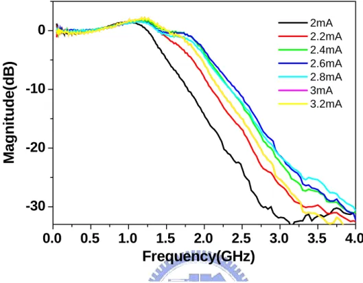
2.3.3 Results and Discussion
The small signal response of VCSELs as a function of bias current was measured at 25oC using a calibrated vector network analyzer (Agilent 8720ES). Fig. 2-8 indicates the modulation frequency increases with the bias current low current range. At a bias current of larger than 2.5mA, the bandwidth saturate and the maximum 3dB modulation frequency response is measured as ~2 GHz. In Fig. 2-9, the 3dB bandwidth (f3dB) is plotted as a function of the bias current. At low bias currents, the
bandwidth increase in proportion to the square root of the current as expected from the rate equation analysis. The saturation of bandwidth was clearly observed as bias current increases above 2.5mA which might be attributed to heating effect. Carrier de-population in QDs subjected to the heated active region may suppress the material gain and put the intrinsic limit of high speed modulation. The modulation current efficiency factor (MCEF) is ~ 2.5 GHz/(mA)1/2. Improvement can be done by increasing the quantum dots stacks and reducing the current density of each dot simultaneously. Finally, we illustrate the eye diagram at 1.25 Gb/s and 2.5 Gb/s, as shown in Fig 2-10. The QD VCSEL shows clear and symmetrical eye diagram at 1.25 Gb/s. At 2.5 Gb/s, the eye was degraded due to the overshoot and insufficient bandwidth. Future work will focus on enhancement of high speed performance by reducing the device parasitic and thermal impedance.
2.4 Conclusion
We present monolithic quantum-dot vertical-cavity surface-emitting laser (QD VCSELs) operating in the 1.3 µm optical communication wavelength. The QD VCSELs have adapted fully doped structure on GaAs substrate. The output power is ~ 330 µW with slope efficiency of 0.18 W/A at room temperature. Single mode operation was obtained with side-mode suppression ratio of > 30 dB. The high speed characteristics were also investigated. The free running bandwidth of QD VCSEL is ~2GHz. The modulation current efficiency factor (MCEF) is ~ 2.5 GHz/(mA)1/2. Finally, we illustrate the eye diagram at 1.25 Gb/s and 2.5 Gb/s.
Reference
[1]H. C. Yu, S. J. Chang, Y. K. Su, C. P. Sung, Y. W. Lin, H. P. Yang, C. Y. Huang and J. M. Wang, “A simple method for fabrication of high speed vertical cavity surface emitting lasers,” Materials Science Engineering B, vol. 106, pp. 101-104, 2004.
CCD Objective Keithley 238 driver Power supply Power meter Spectrum analyzer Computer Integrating sphere PD Prober 0.0 0.5 1.0 1.5 2.0 2.5 3.0 3.5 0 2 4 6 8 10 12 14 16 18 20 V o lt age (V) 0.00 0.05 0.10 0.15 0.20 0.25 0.30 0.35 Po w e r ( m W) 0.0 0.5 1.0 1.5 2.0 2.5 3.0 3.5 0 2 4 6 8 10 12 14 16 18 20 V o lt age (V) 0.00 0.05 0.10 0.15 0.20 0.25 0.30 0.35 Po w e r ( m W)
1272
1274
1276
1278
1280
1282
-80
-70
-60
-50
-40
-30
-20
-10
4mA 1.6mAIn
ten
s
it
y
(d
B
m
)
Wavelength(nm)
1.6mA 2 mA 2.6mA 3.2mA 3.8mA 4 mA1272
1274
1276
1278
1280
1282
-80
-70
-60
-50
-40
-30
-20
-10
4mA 1.6mAIn
ten
s
it
y
(d
B
m
)
Wavelength(nm)
1.6mA 2 mA 2.6mA 3.2mA 3.8mA 4 mA 0.0 0.5 1.0 1.5 2.0 2.5 3.0 3.5 0.00 0.05 0.10 0.15 0.20 0.25 0.30 0.3550
oC
20
oC
Po
wer
(mW
)
Current (mA)
20
oC
25
oC
30
oC
35
oC
40
oC
45
oC
50
oC
Current driver Network analyzer
Laser diode Photodetector
0 5 10 15 20 -65 -60 -55 -50 -45 -40 -35 -30 -25 -20 -15 -10 -5 R espon s e ( d B ) Frequency (GHz) S11 : Reflection coefficient S21: Frequency response HP 8720ES VNA New Port 525 New Focus 1414 Bias Tee QD VCSEL
Fiber
0.0
0.5
1.0
1.5
2.0
2.5
3.0
3.5
4.0
-30
-20
-10
0
Ma
g
n
it
ude
(d
B)
Frequency(GHz)
2mA 2.2mA 2.4mA 2.6mA 2.8mA 3mA 3.2mA0.0
0.2
0.4
0.6
0.8
1.0
1.2
0.0
0.5
1.0
1.5
2.0
MCEF=2.5 GHz/(mA)
1/23-dB F
re
q
uency (
GH
z
)
(I - I
th)
1/2(mA)
1/2Fig. 2-8 Small signal modulation response of QD VCSEL
Fig.2-10 Eye diagram of the QD VCSELs at (a) 1.25 Gb/s and (b)
2.5 Gb/s ( The time scale was 200 ps/div and 100 ps/div) (b)
Chapter 3 Injection Locking of Quantum Dot VCSEL
This investigation experimentally demonstrates the dynamic characteristics of quantum dot vertical-cavity surface-emitting lasers (QD VCSEL) without and with light injection. The QD VCSEL is fully doped structure on GaAs substrate and operates in the 1.3 µm optical communication wavelength. The eye diagram, frequency response, and intermodulation distortion are presented. We also demonstrate that the frequency response enhancement by light injection technique allows us to improve the performance of subcarrier multiplexed system.
3.1 Modulation Response Enhancement by injection locking technique 3.1.1 Theory:Injection Locking Theorem
A rate equations based model is usually used to describe the interaction between photons and carriers inside a laser cavity. When an additional light source is injected into the cavity, the system preserves the general form of the original equations, but with extra terms describing the effects of the injection [1]. These extra terms play an important role in this nonlinear dynamic system and the equations are shown below.
n n inj c th s sp inj c p F S S N N G N e I dt dN F t S S k w N N G dt d F R t S S k S S N N G dt dS + ⋅ + − − − = + ∆ ⋅ + ∆ − − = + + ∆ ⋅ ⋅ + − + − = ε τ φ α φ φ τ ε φ 1 ) ( )) ( sin( ) ( 2 )) ( cos( 2 ] 1 1 ) ( [ 0 0 0 0 0
In these equations, S,φ, and N denote the photon number, the phase, and the carrier number inside the follower laser cavity, respectively. G0 denotes the gain coefficient,
N0 is the transparency carrier number, τp and τn are the photon and carrier lifetimes,
respectively, I is the follower laser bias current, ε is the gain compression factor, and α is the linewidth-enhancement factor. Rsp is the spontaneous emission rate and the
Langevin noise terms F are also added for completeness. And ∆φ(t)=φinj-φ(t) The
follower laser locks to the master only for a certain combination of the injection power and frequency detuning. The stable locking condition can be found as [2]
S S k w S S kc inj + <∆ < c inj − 1 α2
rThe presence of the linewidth-enhancement factor makes the follower laser easier to lock to a master laser at the red side and, therefore, the locking range is asymmetric in frequency detuning. Also, a higher injection power results in a larger locking range. If the detuning range is mapped out for different injection powers, we obtain the locking range of the system.
We begin by assuming a steady-state value for each of the variables with a small signal modulation term, at the optical frequency
jwt jwt jwt jwt N N jwt jwt s s e w N N N e w e w S S S e w F F e w F F e w F F ) ( , ) ( , ) ( ) ( , ) ( , ) ( 1 0 1 0 1 0 + = + = + = = = = φ φ φ φ φ Substituting (3.2) into (3.1),
Only considering the small- signal modulation terms in (3.2) for the photon part,
) ( )) ( ) sin( ) cos( 2 ) ( ( 2 ) ( 1 ) ( ) 1 1 )( ( 1 ) ( ) ( 1 0 0 0 1 0 1 0 0 1 0 0 0 1 0 0 0 1 w F w S S w S S S k e w S S S w N G S S w S S N N G w iwS s inj inj inj inj c p iwt tr + − − − + − + + + − + − = φ φ φ φ φ τ ε ε ε ε
Similarly, for the phase term, considering the small-signal modulation terms in (3.2),
) ( )) ( ) cos( ) sin( 2 ) ( ( ( 2 ) ( ) ( 1 0 0 1 0 1 0 1 w F w w S S S k w N G w
iwφ =α − c inj − φ −φinj + φ −φinj φ + φ
(3-2)
) ( 1 ) ( ) 1 1 )( ( 1 ) ( ) ( ) ( 0 0 1 0 0 0 1 0 0 0 1 1 S F w S w N G S S w S S N N G e w N w iwN tr n s iwt + + − + − + − − − = ε ε ε ε τ
Equations (3.3), (3.4), (3.5) can now be written in matrix form:
⎥ ⎥ ⎥ ⎦ ⎤ ⎢ ⎢ ⎢ ⎣ ⎡ = ⎥ ⎥ ⎥ ⎦ ⎤ ⎢ ⎢ ⎢ ⎣ ⎡ N s F F F N S A φ φ 1 1 1 ⎥ ⎥ ⎥ ⎥ ⎥ ⎥ ⎥ ⎥ ⎥ ⎥ ⎥ ⎥ ⎥ ⎥ ⎦ ⎤ ⎢ ⎢ ⎢ ⎢ ⎢ ⎢ ⎢ ⎢ ⎢ ⎢ ⎢ ⎢ ⎢ ⎢ ⎣ ⎡ + + + + − + − − − + − − + − − − − + + − + − − = s tr inj inj c inj inj c inj inj c inj inj c p tr S S G iw S S S N N G G S S k iw S S k S S G S S k S S k S S S N N G iw A τ ε ε ε ε α φ φ φ φ ε φ φ φ φ τ ε ε ε 1 1 0 ) 1 1 ( 1 ) ( 2 ) cos( ) sin( 2 1 ) sin( 2 ) cos( 1 ) 1 1 ( 1 ) ( 0 0 0 0 0 0 0 0 0 0 0 0 3 0 0 0 0 0 0 0 0 0 0 0 0 0
The small-signal modulation response can also be found from this system by considering I as the small signal modulation current.
⎥ ⎥ ⎥ ⎦ ⎤ ⎢ ⎢ ⎢ ⎣ ⎡ = ⎥ ⎥ ⎥ ⎦ ⎤ ⎢ ⎢ ⎢ ⎣ ⎡ − I A N S 0 0 1 1 1 1 φ
The modulation response transfer function will be ) ( ) ( ) ( 1 w I w S w H =
Based on the above analysis, the small signal modulation response of the injection locked laser has been shown to be of the same form as that of a free-running laser with an additional 1st order pole :
γ a s s H + − ⋅ + ∝ + + + + ∝ 2 2 2 3 0 1 1 1 ) ( (3-5) (3-6)
In this equation, s = jw and K represents he 1st order pole introduced by the injection, wR the resonance and the damping term. The coefficients ai and bi are functions of the
laser parameters and injection conditions [3].
The frequency response of this system is simplified considerably when Sinj=0 (i.e. no
injected light). In this case, a0=b0=0, and the frequency response in equation (3-6) is
reduced to . ) ( ) ( 1 ) ( 1 2 2 b jw b jw A w H + +
= This is the familiar two-pole equation for a directly modulated laser and the relaxation oscillation frequency is
P N
r b a S
f =(2π)−1 1 ~(2π)−1 τ
On the other hand, when Sinj/S is very large, b0 becomes negligible compared to the
other terms in the denominator of the transfer function, which is once again reduced
to a two-pole function, . ) ]( ) ( ) [( ) ( 1 2 2 0 jw b jw b jw a jw A w H + + + = with now S S k b1 ≈− c2 inj and π 2 1 b
fr = . This is very interesting as it seems to indicate that
3.1.2 Experimental Setup:Injection Locking System
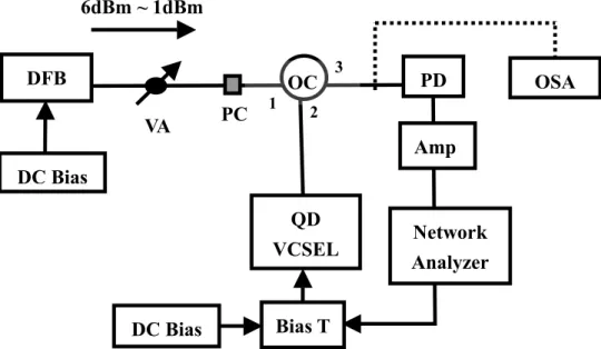
The experimental setup is schematically illustrated in Fig.3-1. The QD VCSEL is used as the slave laser while a DFB laser is used as the master laser. The injection power is varied by a variable optical attenuator at the output of the DFB laser. The polarization of the DFB laser is adjusted using a polarization controller before injecting into the QD VCSEL. The adjusted DFB laser signal injects into the port 1 of optical circulator then injecting into QD VCSEL at the port 2. The QD VCSEL is directed modulated by vector network analyzer. The light output at port 3 of optical circulator is divided into 2 parts. 90% of the light signal is transmitted into photo detector then convert into electrical signal amplified by RF amplifier and sent into vector network analyzer to measure frequency response. 10% of the light signal is connected to optical spectrum analyzer to observe the locking condition. In the experiment, the polarization and the center wavelength of DFB laser are adjusted that the QD VCSEL has the most significant enhancement in the frequency response. The wavelength detuning is adjusted by changing the temperature and bias current of DFB laser.
3.1.3 Results and Discussion
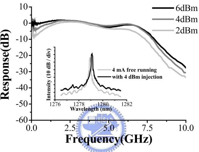
The free running frequency response of the QD VCSEL is shown as Fig.3-2 and the inset of Fig.3-2 shows the spectra of QD VCSEL. Fig. 3-3 shows the frequency response of the QD VCSEL with light injection and the QD VCSEL is biased at 4 mA. The detuning wavelength (λDFB-λQD VCSEL) is 0.128nm. This figure clearly shows
that external light injection can achieve a significant enhancement in frequency response. When the power injection is 6dBm, the 3-dB frequency is from 1.75GHz to 7.44GHz which is the most improved bandwidth. The inset of Fig.3-3 is the spectra of QD VCSEL with and without light injection. After injection locking, the wavelength
QD VCSEL and the power level of QD VCSEL light output is enhanced by external light injection. We plot the 3dB frequency verses injection power as shown in Fig. 3-4. In this figure, we can observe that the 3dB frequency is enhanced by injection power of DFB laser. This is because external light injection in the active region of QD VCSEL makes the photon number increase thus improving the 3dB bandwidth. To prove the improved bandwidth can be utilized, we also demonstrated that this enhancement of the frequency response can greatly improve the performance of SCM system based on direct modulation of QD VCSELs.
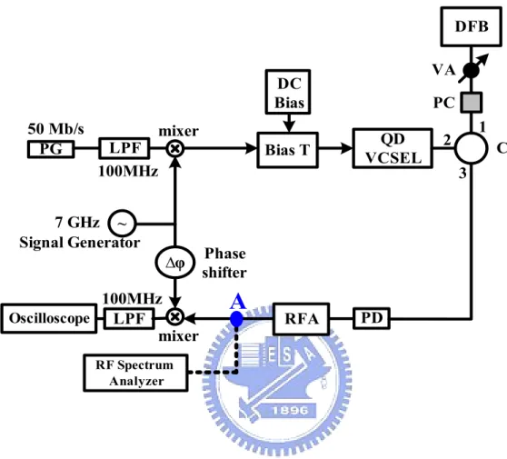
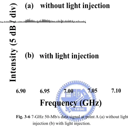
. Fig. 3-5 shows the experimental setup for the injection locking of QD VCSEL in a SCM system. A 50 Mb/s non-return-to-zero (NRZ) pseudo-random binary sequence (PRBS) data with 231 – 1 pattern length from a pattern generator is mixed with a 7 GHz RF carrier. The resulting data signal is then used to directly modulate the QD VCSEL. Fig.3-6 shows the electrical spectra of QD VCSEL with and without light injection at point A. Light injection technique leads to 33 dB improvement in the SCM system. The 7-GHz 50-Mb/s is down converted using a mixer, where it is mixed with the same RF carrier generated by the signal generator. The variable phase shifter is used to adjust the carrier’s phase. The corresponding eye diagrams are shown in Fig. 3-7. The improvement in system performance can be clearly seen when light injection technique is employed. The QD VCSEL without light injection cannot generate 7-GHz 50-Mb/s data due to the limited frequency response.
3.2 Reduction of nonlinear distortion by injection locking technique
We also study the reduction of nonlinear distortion in the QD VCSEL by light injection technique. Nonlinear distortion of the laser is important consideration for
SCM systems, the IMD3 has the largest impact on performance degradation because of the IMD3 signal close to the original subcarrier frequencies [4].
3.2.1 Theory
The goal of any transmission system is to transfer information as accurately as possible. However, neither device is perfectly linear, particularly when large modulation levels are involved. Several different types of distortion products are common from these components such as harmonic distortion and intermodulation distortion.
When laser is intensity modulated there will be modulated signal power at he modulating frequency; and depending on the linearity of the device, there will also be some modulating power at harmonics of the modulating frequency. Some modulated power at the second harmonic and third harmonic of the modulating frequency is very common. Harmonic distortion is defined as the ratio of modulated power in harmonic of the modulating frequency to the power at the modulating frequency. For example:
) ( ) 2 ( mod mod 2 f P f P HD = ) ( ) 3 ( mod mod 3 f P f P HD = ) ( ) ( ... ) 3 ( ) 2 ( mod mod mod mod f P nf P f P f P THD= + + +
where HD2 is the second harmonic distortion, HD3 is the third harmonic distortion,
and THD is the total harmonic distortion[5].
It is common to express the distortion in decibels (dB). In this case, the harmonic distortion is expressed as:
) ) ( ) ( log( 10 mod mod f P xf P HDx =
Intermodulation distortion (ID) occurs when two or more modulating signals are present. In this case, device nonlinearities cause the two modulating signals to interact,
intermodulation distortion for two signals can e measured as: ) ( ) ( ) ( 2 i j i j i f P f f P f f ID ± = ± where P(fi)=P(fj).
A particularly distressing form of intermodulation distortion is third-order intermodulation (IMD) for two closely spaced signals. This is because the IMD signals fall close to the original modulating frequencies.
) ( ) 2 ( ) 2 ( i j i j i f P f f P f f IMD − = − 3.2.2 Experimental Setup
Fig. 3-8 shows the experimental setup for measuring the IMD3 of QD VCSEL with and without light injection. A commercial DFB laser is used as the master laser in our experiments. The injection power is controlled by a variable optical attenuator at the output of the DFB laser. The polarization of the DFB laser is adjusted using a polarization controller. The polarization is chosen that the second harmonic distortion of QD VCSEL has the must reduction. An optical circulator is used to couple the DFB laser light into the QD VCSEL. The QD VCSEL is modulated as single tone or two tone measurements by RF signal generator.
3.2.3 Results and Discussion
Fig. 3-9 (a) shows the electrical spectrum of the QD VCSEL without light injection under a 1 GHz microwave modulation. The microwave power level before the bias-T is 3 dBm. The second harmonic distortion of the QD VCSEL without light injection is -8.2 dB. Fig. 3-10 (b) shows the corresponding spectrum of the QD VCSEL with light injection. The central wavelength of DFB laser is 1277.99 nm, and the injection power is 2 dBm. The second harmonic distortion has been dramatically reduced to
distortion of QD VCSEL with light injection has been suppressed by more than 14 dB from 100 MHz to 1.2 GHz.
Two-tone measurements without and with light injection varied with the input RF power is also investigated, as shown in Fig. 3-10. The two-tone frequencies are 1 and 1.01 GHz. The fundamental tone power increase of 4.5dB and the distortion suppression of 10.6 dB are observed. As a result, the dynamic range of the QD VCSEL with light injection can be enhanced 15.1 dB for the IMD3.
3.3 Conclusion
In this chapter, we report the dynamic characteristics of QD VCSEL without and with external light injection. The significant enhancement of frequency response by light injection technique has been studied. The 3 dB frequency response has been increased by as much as 4.2 times using light injection technique. Moreover, this frequency response enhancement can improve the performance of SCM system. Experimental results show a 33 dB improvement in system performance. Furthermore, reduction of IMD3 in the QD VCSEL also has been observed. The dynamic range of the QD VCSEL with light injection can be enhanced 15.1 dB for the IMD3.These results show that external light injection is a very powerful technique to upgrade QD semiconductor lasers.
Reference
[1] N. Schunk and K. Petermann, "Noise analysis of injection-locked semiconductor injection lasers," IEEE Journal of Quantum Electronics, vol. QE-22, pp. 642-50,1986.
[2] C. H. Henry, N. A. Olsson, and N. K. Dutta, “Locking range and stability of injection locked 1.54-_m InGaAsP semiconductor lasers,” IEEE J. Quantum
Electron., vol. QE-21, pp. 1152–1156, Aug. 1985.
[3] Lukas Chrostowski, Optical Injection Locking of Vertical Cavity Surface Emitting Lasers (A dissertation for the degree of Doctor of Philosophy, 2003).
[4] W. I. Way, Broadband Hybrid Fiber/Coax Access System Technologies (Academic Press, San Diego, 1999).
0.0
2.5
5.0
7.5
10.0
-60
-50
-40
-30
-20
-10
0
10
R
esp
on
se (d
B
)
Frequency (GHz)
3mA
3.5mA
4mA
OC Amp Network Analyzer PD QD VCSEL DC Bias PC Bias T DFB VA 1 2 3Fig. 3-1 (a) Schematic diagram of the quantum dot vertical cavity surface emitting laser (b)
Experimental setup for the injection locking of QD VCSEL (DFB: DFB laser, VA: variable optical attenuator, OC: optical circulator, OSA: optical spectrum analyzer, PC: polarization controller, PD: photodetector, Amp: electrical amplifier)
DC Bias 6dBm ~ 1dBm OSA 1276 1278 1280 1282 -70 -60 -50 -40 -30 -20 -10 0 In te ns ity (1 0 d B / d iv ) Wavelength (nm) 3mA 3.5mA 4mA
0.0
2.5
5.0
7.5
10.0
-60
-50
-40
-30
-20
-10
0
10
Re
sp
on
se
(d
B)
Frequency(GHz)
6dBm
4dBm
2dBm
1276 1278 1280 1282 -70 -60 -50 -40 -30 -20 -10 0 Intensity (10 dB / d iv) Wavelength (nm) 4 mA free running with 4 dBm injection0
2
4
6
8
10
12
3 dB Frequency (
G
Hz)
PG 50 Mb/s ~ 7 GHz ∆φ shifterPhase QD VCSEL LPF 100MHz Signal Generator DC Bias LPF 100MHz Oscilloscope mixer PD
A
DFB Bias T PC 1 2 3 VA RFA mixer C RF Spectrum AnalyzerFig. 3-5 Experimental setup for the quantum dot VCSEL without and with light injection in a subcarrier multiplexed system. (PG: pattern generator, LPF: low pass filter, RFA: RF amplifier, PD: photodetector)
without light injection
with light injection
In
te
ns
it
y (
5 dB
/ di
v)
6.90
6.95
7.00
7.05 7.10
Frequency (GHz)
(b)
(a)
Fig. 3-6 7-GHz 50-Mb/s data signal at point A (a) without light
C RF Spectrum Analyzer PD QD VCSEL DC Bias PC Bias T DFB VA 1 2 3 DC Bias RF Signal Generator f2 f1 f2 f1 Fundamental IMD3 Fundamental RFA
Fig. 3-8 Experimental setup for measuring the third-order
intermodulation distortion (IMD3) of quantum dot VCSEL without and with light injection.
-8.2 dB
Without light injection
-26.4 dB
With light injection
Intensity (5 dB / div)
0.5 1 1.5 2 2.5
Frequency (GHz)
(b)
(a)
0.0
0.4
0.8
1
-70
-60
-50
-40
-30
-20
-10
0
Without light injectio
With light injection
Second H
am
oni
c D
istri
buti
on (dB)
(c)
-15
-10
-5
0
5
-120 -100 -80 -60 -40 -20 0without light injection Fundametal IMD3
with light injection Fundametal IMD3
Ou
tp
ut
Po
we
r (d
Bm)
RF Input Power (dBm)
Chapter 4 Slow Light in Quantum Dot VCSEL
This investigation experimentally demonstrates tunable slow light in a 1.3 µm quantum dot vertical-cavity surface-emitting laser (QD VCSEL) at 10 GHz. The QD VCSEL fabricated on a GaAs substrate is grown by molecular beam epitaxy with fully doped n- and p-doped AlGaAs distributed Bragg reflectors. Tunable optical group delays are achieved by varying the bias currents, and the maximum delay of 42 ps at 10 GHz has been demonstrated at room temperature. Moreover, the delay-bandwidth product is 0.42.
4.1 Theory: Approaches to achieve slow light
To obtain a slow light device, in general, one must vary the medium within which the optical signal travels by either increasing the path length or reducing the signal group velocity. The former can be accomplished with the use of a fiber delay line, which will be discussed below. The latter has several possibilities. We first observe that the group velocity is defined as
where n is real part of the refractive index and k is the waveguide propagation constant. We can define a slowdown factor S as
k n c w w n w n v c S g ∂ ∂ − ∂ ∂ + = = 1
From (4-2), we see that the group velocity can be reduced by introducing a large and positive waveguide dispersion n
∂ ∂ or material dispersion n ∂ ∂ . The waveguide w n w n k n w c k w vg ∂ ∂ + ∂ ∂ − = ∂ ∂ = (4-1) (4-2)
also possible to include both material and waveguide dispersion in one device to have an enhanced effect [2].
a. Optical Fiber Delay Lines:
Optical fiber delay lines have previously been referred to as an “optical buffer” [3]. One basic design typically consists of a 2×2 optical switch connected with a fiber loop. Other components such as optical isolators, amplifiers, and dispersion compensation devices have also been included to reduce impairments due to reflection, loss, and dispersion.
The optical switch is first set to direct the data train into the fiber loop and subsequently is closed to allow the data to recirculate in the loop. The storage capacity, i.e., amount of data stored, is limited by the time required to travel one loop τloop subtracted by that required to set the switch. This is because when the optical
data stream is longer than τloop, the data of the leading part of the packets will overlap
with that in the back to cause interference. The storage time, i.e., how long the data is kept in the loop, is an integer multiple of. The turn-off (release) time is also determined by τloop. This is because once a packet enters the delay line, it can only
emerge at a fixed duration of time later. It is impossible to remove the packet from the delay line before that fixed time interval.
b. Slow Light Using Waveguide Dispersion:
Studies on the light propagation in highly dispersive structures with a very slow group velocity have drawn much attention. Grating structures have been used extensively in DFB lasers and grating waveguide couplers. Recent progress on the fabrication of grating structures in fiber has opened new research areas using fiber Bragg gratings [4]. Recently, another method for achieving slowed light based on a Moiré fiber Bragg grating has been suggested [5]. A Moiré grating is formed if the
) 2 cos( ) 2 cos( ) ( 0 Λ Λ + = z s z n n z n δ π π
where Λ is the Bragg period and Λ s is the Moiré period. The theoretical analysis shows that the group velocity of light in the transmission band can be slowed down substantially although with a very small signal bandwidth.
c. Progress in EIT-Based Slow Light:
EIT refers to an artificially created spectral region of transparency in the middle of an absorption line due to the destructive quantum interference arising from two transitions in a three-level system [6], [7]. There are three basic energy level schemes for implementing a three-level EIT system interacting with two near-resonance electromagnetic fields. In a ladder or cascade system, levels are arranged as E1<E2<E3; in a V scheme, levels are arranged as E2<E1 and E3; whereas in a scheme, levels are arranged as E1, E3 <E2. In all three cases, we label the transitions the same way: |1> to |2>, and |2> to |3> are strong dipole-allowed transitions, while |1> to |3> is a dipole-forbidden transition.
The signal field connecting |1> to |2> is the light field that one desires to slow down in a controllable fashion. The pump field is the control field connecting |2> to |3>, whose intensity controls the amount of slowing down. In the literature, the pump laser is sometimes called the control laser.
As a result of the coherent coupling between the atomic system and the laser beams, atomic levels |1> and |2> are no longer eigenstates of the system. Instead, they are dressed by the pump laser and become two new states |2d> and |3d>. This (destructive) quantum interference between two absorption paths produces a transparency spectral window in the middle of the strong |1> to |2> absorption line. The width of this (4-3)