國 立 交 通 大 學
顯示科技研究所
碩 士 論 文
藉由波導耦合之金領結結構捕捉奈米粒子
Trapping nano-sized particle by
waveguide-coupled gold bowtie structure
研 究 生 :朱恒沂
指導教授:李柏璁 博士
藉由波導耦合之金領結結構捕捉奈米粒子
Trapping nano-sized particle by
waveguide-coupled gold bowtie structure
研究生:朱恒沂 Student:Heng-Yi Chu
指導教授:李柏璁 Advisor:Dr. Po-Tsung Lee
國 立 交 通 大 學
顯示科技研究所
碩 士 論 文
A ThesisSubmitted to Department of Photonic and Display Institute College of Electrical Engineering and Computer Science
National Chiao of the Requirements for the Degree of Master
in
Electro-Optical Engineering October 2013
Hsinchu, Taiwan, Republic of China 中華民國 102 年 10 月
I
藉由波導耦合之金領結結構捕捉奈米粒子
研究生:朱恒沂 指導教授:李柏璁 博士
國 立 交 通 大 學
顯示科技研究所
摘要
我 們 提 出 一 個 以 波 導 偶 合 激 發 侷 域 化 表 面 電 漿 共 振 之 粒 子 捕 捉 系 統 , 此 系 統 具 有 尺 度 小 以 及 容 易 整 合 於 晶 片 之 優 點 , 包 含 以 金 為 材 料 的 領 結 結 構 以 及 氮 化 矽 波 導 。 由 模 擬 結 果 預 測 , 領 結 結 構 的 間 隙 處 具 有 集 中 且 增 強 的 場 分 布 , 可 產 生 強 大 的 光 學 鉗 制 力 以 捕 捉 微 觀 尺 度 的 物 體 。 我 們 發 現 具 5 奈 米 間 隙 領 結 結 構 在 1.55 微 米 波 長 激 發 下 能 對 20 奈 米 聚 苯 乙 烯 粒 子 產 生 高 達 1389pN/W 的 光 學 鉗 制 力 。 在 實 驗 中 為 了 直 接 觀 測 , 我 們 以 1 微 米 的 聚 苯 乙 烯 粒 子 驗 證 此 系 統 的 粒 子 捕 捉 能 力 , 觀 測 到 此 粒 子 沿 波 導 移 動 最 後 被 領 結 結 構 捕 捉 的 完 整 現 象 , 並 於 關 閉 耦 合 光 源 後 觀 測 到 粒 子 被 釋 放 並 漂 離 的 現 象 。 未 來 將 此 捕 捉 系 統 與 其 他 感 測 分 析 系 統 一 同 整 合 於 晶 片 上 將 能 實 現 生 物 晶 片 的 目 標 。II
Trapping nano-sized particle by
waveguide-coupled gold bowtie structure
Student:Heng-Yi Chu Advisor:Dr. Po Tsung Lee
Department of Photonics & Display Institute
National Chiao Tung University
Abstract
We propose a particle manipulation system by using localized surface plasma resonance excited by a coupling waveguide. The system, featured with advantages such as small footprint and easily being integrated in a chip, is composed of gold bowtie and silicon nitride waveguide. The simulation shows highly concentrated and enhanced field in gap of the bowtie where strong optical trapping force will be established and will be able to trap microscopic particles. We find a bowtie with 5 nm gap at the tips can provide 1389 pN/W force for trapping 20 nm polystyrene particle under excitation at 1.55 μm wavelength. For direct observation in experiment, we use 1 μm polystyrene particle to verify trapping ability of the system. We see the particle transported along the waveguide and finally being trapped stably by the bowtie. We also see release of the particle which swims away after the excitation light source is turned off. In the future, this system can be integrated with other sensing and analyzing systems to realize lab on a chip.
III
Acknowledgements
老師,謝謝您兩年多來的關心照顧,在您輕鬆的教導與嚴格的要求下,讓我有機會學 習時間管理、資料搜尋和獨立思考的觀念,讓我具備了信心與勇氣面對未來的挑戰。 感謝林品佐學長在研究上的指導,雖然我資質駑鈍,但您仍不厭其煩的解答我的疑 問,並且在您大力幫忙下,讓我得以順利的完成實驗。另外也要謝謝盧贊文學長、蔡家 揚學長、林佳裕學長、張開昊學長在研究上的建議與生活上的關心。此外也要謝謝郭光 揚學長和黃品睿學姊在我鬱悶煩惱時讓我轉移注意力,幫助我調適心情。謝謝蔡為智學 長、吳哲堯學長和劉權政學長在趕著畢業之餘仍耐心地將實驗技巧傳承予我。謝謝陳佑 政和林宜錩同學陪伴我一起度過艱苦的時光。同時也麻煩了聰明乖巧的學弟鄭聖諺和許 擇恩,在我繁忙的時候幫我分擔許多實驗。謝謝學弟鍾坤達和張家瑞平日在實驗室給予 大家的歡樂,讓我能在快樂的心情下做研究。此外,也感謝實驗室排球運動時間,使我 在沉重的課餘間外,能夠鍛鍊身體並放鬆心情。 謝謝我的家人,讓我無後顧之憂的栽進這兩年的研究生活,謝謝你們的關懷與照顧, 幫我解決各種生活上的困難,在我挫折跌倒時,給予庇護的港灣,使我能恢復過來並重 新往前邁進。 最後,兩年的學園生活,在時間流逝下忡忡的過去了。有許多的不捨、有無盡的回 憶、有數不清的歡樂時光,謹以此頁致敬。 朱恒沂 2013年10月 謹誌於 新竹交通大學 交映樓IV
Table of contents
Abstract (in Chinese) ... I
Abstract (in English) ... II
Acknowledgements ... III Table of contents ... IV Figure Captions ... IV Table Captions ... X Chapter. 1 INTRODUCTION ... 1 1-1 LAB ON CHIP SYSTEM ... 1
1-2 PARTICLE MANIPULATION IN THE OPTICAL NEAR-FIELD ... 3
1-2-1 Method for calculating optical force ... 3
1-2-2 From dielectric to metal structures ... 6
1-2-3 Merits of LSPR for particle manipulation ... 7
1-3 MOTIVATION ... 10
Chapter. 2 STRUCTURE DESIGN AND NUMERICAL CHARACTERIZATION ... 11
2-1 OPTICAL FORCE ANALYSIS... 11
2-2 FINITE ELEMENT METHOD ... 15
2-3 GOLD BOWTIE STRUCTURE DESIGN FOR PARTICLE TRAPPING ... 17
2-3-1 Enhancement provided by gap structure ... 18
2-3-2 Dependence on gap size ... 24
2-3-3 Consideration for fabrication ... 26
2-4 SUMMARY ... 31
Chapter. 3 FABRICATION AND MEASUREMENT ... 32
3-1 FABRICATION PROCESS ... 32
V
3-3 SPECTRAL ANALYSIS ... 39
3-4 DEMONSTRATION OF TRAPPING ... 42
3-5 SUMMARY ... 44
Chapter. 4 CONCLUSION AND FUTURE WORK ... 45
4-1 CONCLUSION ... 45 4-2 FUTURE WORK ... 47 Appendix A ... 49 Appendix B ... 50 Appendix C ... 51 Reference ... 52
VI
Figure Captions
Fig. 1-1 Ray optics description of the gradient force (Adapted from reference [1]). ... 3 Fig. 1-2 Schematic illustration of (a) slot waveguide (b) nanoslot waveguide photonic crystal
cavity (Adapted from reference [24][25]). ... 7 Fig. 1-3 illustration of the integrated bow-tie like plasmonic tweezers on optical waveguide
in cross-section view and top view ... 7 Fig. 1-4 (a) The field intensity in front of the open end of the rectangular waveguide. (b) The
field intensity measured 0.5 cm in front of the bowtie (Adapted from reference [28]). ... 8 Fig. 1-5 |E|2 enhancement vs wavelength and scattering efficiency (Qscat) vs wavelength for
16nm gap and 160nm gap (Adapted from reference [29]). ... 9 Fig. 2-1 The simulated model(a) before (b) after mesh generation of Comsol multiphysics
software. ... 12 Fig. 2-2 Force integration over object surface of Comsol software. ... 13 Fig. 2-3 Schematic illustration of our trapping system with structural parameters and
coordinates indicated. ... 17 Fig. 2-4 (a) Illustration of particle position in cross-section view and top view. (b) Fz acting
on the PS particle as a function of incident wavelength for single triangle and bowtie. ... 19 Fig. 2-5 (a) The field enhancement from (0, 0, 30 nm) to (0, 0, 60 nm) for single triangle and
bowtie. Insets show cross-section view of the electric field intensity (b) The field enhancement from y = -40 to y = 40nm (x = 0, z = 30 nm) for single triangle and bowtie. Insets show top view of the electric field intensity. The incident wavelength is 1.55 μm... 20 Fig. 2-6 (a) Fz acting on the PS particle as a function of position along the z axis (x = y = 0).
(b) Fx as a function of location along the axis of (x, 0, 45 nm) (indicated by red arrows in top-view schematic). (c) Fy as a function of position along the axis of (0, y, 45 nm) (indicated by green arrows in top-view schematic). ... 21 Fig. 2-7 (a) Illustration of particle position in cross-section view and top view.(b) Fx acting
on the PS particle as a function of location along the axis of (x, 0, 15 nm). The position in which particle can’t enter is fitting by dash line. ... 22
VII
Fig.2-8 The potential along three axis by integrated the trapping force Fz, Fx and Fy along the z, x, and y axis. ... 23 Fig. 2-9 (a) Simulated spectra of Fz exerted upon the particle trapped by the bowtie structure
with gap size varied from 5 nm to 90 nm, r = 0, D = 300 nm, t = 30 nm, and α = 90°. (b) Summarizing peak wavelength with gap size. (c) Summarizing peak force Fz with gap size. ... 24 Fig. 2-10 The top view of electric field intensity for (a) gap size=5 nm, λ=1.55 μm. (b) gap
size=30 nm, λ=1.4 μm. (c) gap size=60 nm, λ=1.33 μm. (d) gap size=90 nm, λ=1.3 μm. ... 25 Fig. 2-11 (a) Simulated spectra of Fz exerted upon the particle trapped by the bowtie
structure with r varied from 5 to 50 nm, α = 90°, D = 300 nm, t = 30 nm, and g = 5 nm. (b) Summarizing peak wavelength with ROC. (c) Summarizing peak force Fz with ROC. ... 27 Fig. 2-12 Simulated spectra of Fz exerted upon the particle trapped by the bowtie structure
with D varied from 300 to 350 nm, α = 90°, r = 10 nm, t = 30 nm, and g = 30 nm. .. 28 Fig. 2-13 (a) Fz acting on the PS particle as a function of position along the z axis (x = y = 0).
(b) Fx as a function of location along the axis of (x, 0, 15 nm) (indicated by red arrows in top-view schematic). (c) Potential along z axis by integrated the trapping force Fz. (d) Potential along x axis by integrated the trapping force Fx. ... 29 Fig.2-14 (a) Simulated spectra of Fz exerted upon the particle trapped by the bowtie structure
with particle diameter varied from 20 to 1000 nm, α = 90°, r = 10 nm, D = 350 nm, t = 30 nm, and g = 30 nm. (b) Summarizing peak wavelength with particle diameter. (c) Summarizing peak force Fz with particle diameter. ... 30 Fig.2-15 The side view of electric field intensity for 500 nm PS. Inset shows electric field
intensity zooming out along x direction. ... 31 Fig. 3-1 The first part of fabrication process. ... 32 Fig. 3-2 The second part of fabrication process. ... 33 Fig. 3-3 The top view SEM pictures of these structure (a) general process (b) reverse process.
... 34 Fig. 3-4 (a) Top view AFM picture. (b)Top view SEM picture. (c)Line cross section AFM
picture (white line in Fig.3-4(a)). ... 35 Fig. 3-5 (a) Configuration and (b) photography of upright image system ... 38
VIII
Fig. 3-6 The schematic diagram of the thin chamber. ... 39 Fig. 3-7 (a)The extinction spectral of bowtie array on glass substrate with incident light
polarize along y direction. Inset shows SEM picture of bowtie array. (b) The top view of surface change distribution for λ=0.74 μm. (c) The top view of surface change distribution for λ=1.06 μm. ... 40 Fig. 3-8 (a) The extinction spectral of bowtie array with gap size varied from 0 nm to 85nm
on glass substrate (b) Summarizing peak wavelength with gap size. ... 41 Fig. 3-9 Motion of 1 μm particle (indicated by black arrows) as time evolves on 1 μm wide
waveguide in 1.55 μm wavelength and bowtie position indicated by dash line. ... 43 Fig. 3-10 The top view SEM pictures of bowie at trapping site. ... 44 Fig. 4-1 Coupling principle between fiber and photonic wires by means of a grating
(Adapted from reference [35]). ... 47 Fig. 4-2 Setup for waveguide propulsion and Raman spectroscopy (Adapted from reference
[36]). ... 48 Fig. A-1 (a) Simulated spectra of Fz exerted upon the particle trapped by the bowtie structure
with bowtie angle varied from 20° to 90°, r = 0, D = 300 nm, t = 30 nm, and g = 5 nm. (b) Summarizing peak wavelength and peak force with bowtie angle. ... 49 Fig. B-1 (a) Simulated spectra of 20 nm PS particle detection in the gap (0, 0, 15 nm). (b)
Simulated transmission spectra with 20 nm PS particle detection in the slot center. (Adapted from reference [25]) ... 50 Fig. B-2 Simulated spectra of bulk media sensing with n varied from 1.35 to 1.45, α = 90°, D
= 300 nm, t = 30 nm, r = 0 nm and g = 30 nm... 50 Fig. C-1 (a) Simulated extinction spectra and Fz acting on the PS particle as a function of
incident wavelength. (b) Illustration of particle position in cross-section view. (c) Simulated extinction spectra as a function of incident wavelength for z = -750, 0, 15 and 30 nm surface. ... 51
IX
Table Captions
1
Chapter. 1
Introduction
1-1 Lab on chip system
To date, manipulating tiny fragile objects by optical forces with contactless and nondestructive features has inspired many applications ranging from physics to biology. In this field of research, biological particles such as cells, proteins, and viruses are always the target to be manipulated. Prior to various configurations, optical tweezers demonstrated by Ashkin et al. first utilized highly focused laser beam to perform particle trapping [1]. Near the focus, strong optical gradient force is established and attracts objects from all directions. Later, Kawata et al. proposed an unprecedented concept of optical manipulation that particles can be trapped or transported by evanescent wave in the near-field [2, 3]. This started the branch of developing particle manipulation system on a chip. Many devices, such as optical waveguides [4-6] and cavities [7-9], have been proposed featured with small trapping site nearly approaching the limit of diffraction. Thus the manipulation can be more precise and can handle smaller particles compared to conventional optical tweezers. However for further miniaturizing the trapping site, there is still a promising candidate – localized surface plasma resonance (LSPR) in metallic structures, which attract more and more interests recently. In this scheme plasma resonance breaks diffraction limit because the field is induced by resonance of electric carrier at metal surface instead of provided by propagating electromagnetic wave. Therefore structures, such as nano-dot [10], nano-rod [11], nano-ring [12] and nano-bowtie [13], can generate optical forces for trapping particles or molecules down to a few nanometers in size.
2
trapping and manipulation schemes. However, focusing system would confront the optical diffraction limit of propagating wave as the objects become smaller, and the focal spot would become too large to trap nano-sized objects precisely. Also, the gradient optical force decreases fast when scaling down the particle size as a cube fashion of the radius. Therefore, trapping particles smaller than 100 nm in diameter is difficult using either free space optics or evanescent trapping configurations, as high laser powers are needed.
On the other hand, it is common for plasmonic tweezers to use unfocused laser beam through prism to directly illuminate the metallic structures. Although plasmon can be directly excited without prism, using prism can produce evanescent field to confine the target objects close to the surface [14] where LSPR trap sit. Moreover, the evanescent field can be used to guide the object at the interface along the incident in-plane k-vector and consequently to deliver them to the trapping sites without need of any fluidic flow. Conversely, the use of a bulk glass prism is incompatible with the integration into a compact on-a-chip platform in which plasmonic tweezers could be used for trapping biological objects to perform optical inspection.
In this study, we propose a simple optical trapping platform where plasmonic tweezers are integrated on top of a planar optical waveguide coupled to an optical fiber. We aim at transporting target objects along planar waveguide and trapping them at predefined site composed of metallic structure. The vantages of this platform is not only scaling the trap size down to the nanometer-scale but also addressing the integration issue.
3
1-2 Particle manipulation in the optical near-field
1-2-1 Method for calculating optical force
In the research about optical manipulation, optical force is the first thing we want to know. In theoretical analysis, there are two limiting cases for which the force on a particle can be readily calculated. When the trapped particle is much larger than the wavelength of the trapping light, the conditions for Mie scattering are satisfied, and optical forces can be understood from simple ray optics (Fig. 1-1). Refraction of the incident light by the particle corresponds to a change in the momentum carried by the light.
Fig. 1-1 Ray optics description of the gradient force (Adapted from reference [1]).
By Newton’s third law, an equal and opposite momentum change is imparted to the particle. The force on the particle, given by the rate of momentum change, is proportional to the light intensity [15, 16]. It is quite intuitive, but for most interests in biochemical researches, the particle dimensions are always very small. Thus another limiting case, in which the trapped particle is much smaller than wavelength of the trapping light, is more
4
suitable. In this case, the approximation for Rayleigh scattering is satisfied and optical forces can be calculated by treating the particle as a point dipole. The scattering and gradient force components are readily separated. The scattering force is due to absorption and re-radiation of light by the dipole. For a sphere of radius a, this force is
, 1 1 3 128 , 2 2 2 4 6 5 0 m m a c n I F m scatt (1.1) where I0 is the intensity of the incident light, σ is the scattering cross section of the sphere, nm
is the index of refraction of the medium, c is the speed of light in vacuum, m is ratio of refractive index of the particle to refractive index of the medium (np /nm), and λ is the
wavelength of the trapping laser. The scattering force is in the direction of light propagation and is proportional its intensity. The time-averaged gradient force arises from the interaction of the induced dipole with the inhomogeneous field distribution
, 2 0 2 I cn F m grad (1.2) where 2 1 2 2 3 2 m m a nm (1.3) is the polarizability of the sphere. The gradient force is proportional to the intensity gradient, and parallel to the gradient when m > 1. In this limiting case, we can calculate the optical forces exerted on particle from the field distribution simulated without existence of particle. This is very convenient for force calculation and only one simulation process is needed.
However in some near-field optical manipulating structures, particles will encounter sharp field transition around the trapping site. In this situation Rayleigh approximation may
5
be inadequate. Instead, a complete electromagnetic theory is required to supply an accurate analysis [17-23]. And it is the role played by Maxwell stress tensor:
I B H E D HB DE TM * * * * 2 1 (1.4) where Tm represents the Maxwell stress tensor, E is the electric field, B is the magnetic fluxdensity, D is the electric displacement, H is the magnetic field, and I is the isotropic tensor. Since the time recording period is much longer than the period of field oscillation, we prefer to use time-averaged Maxwell stress tensor:
TM DE HB
D E H B
I * * * * 2 1 (1.5) when expended out, the equation becomes ) ( 2 1 ) ( 2 1 ) ( 2 1 H B E D H B E D H B E D H B E D H B E D H B E D H B E D H B E D H B E D H B E D H B E D H B E D T z z z z y z y z x z x z z y z y y y y y x y x y z x z x y x y x x x x x M (1.6)
where the subscripts x, y, and z signify the coordinate directions. By integrating the time-averaged Maxwell stress tensor on the external surface enclosing the particle, we can determine the total electromagnetic force, FEM, acting on the system by
F T n dS S M EM
( ) . (1.7)6
1-2-2 From dielectric to metal structures
In recent years, some groups reported designs for surpassing diffraction limit to reach more concentrated field distribution. For example, Yang et al. [24] demonstrated optical trapping and transportation of dielectric nano-particles by exploiting the strong field within 100 nm slot in a waveguide (Fig. 1-2 (a)). For further improving trapping ability, Lin et al. [25] utilized resonant enhanced optical near-field in a 20 nm slot in photonic crystal (PhC) waveguide cavities to trap particles of nanometer size (Fig. 1-2 (b)). Strong Pseudo-electric field in the nano-slot can generate 200 pN/W optical forces for trapping polystyrene particle of 20 nm diameter. Although nano-slot and PhC cavity altogether can reach excellent field enhancement and trapping ability, the device consists of 53 holes on both sides of the cavity [26]. Therefore the overall footprint is quite large in length of tens of micrometers. Moreover, the 20 nm slot in the cavity is too small to be fabricated by common facilities like electron beam lithography. In the contrary, plasmonic tweezers had been shown that the field enhancement near metallic structures is in nanometer scale attributed to the collective motion of free electrons and field distribution is not limited by diffraction. Besides, trapping particles by the field of LSPR on structure edge is more accessible for trapping particle than the nano-slot. Therefore in this study we aim at addressing integration issue by developing plasmonic tweezers on optical waveguides for particle trapping. Wong et al. had proposed and demonstrated this kind of optical tweezers on waveguides [27]. However the plasmonic structure they use are simple circular metal pads and the utilized evanescent field actually belongs to SPR mode atop the pads instead of LSPR mode. As a result, the trapping site is still extensive and the trapping force is still weak.
7
Fig. 1-2 Schematic illustration of (a) slot waveguide (b) nanoslot waveguide photonic crystal cavity (Adapted from reference [24][25]).
1-2-3 Merits of LSPR for particle manipulation
For taking advantage of LSPR, we will utilize bowtie like metal pads on optical waveguides (Fig. 1-3). Among plasmonic nanostructures, bowtie is most attractive because its triangular geometry will lead to “lightning-rod” effect at apexes.
Fig. 1-3 illustration of the integrated bow-tie like plasmonic tweezers on optical waveguide in cross-section view and top view
8
In 1997, Grober et al .[28] demonstrated that field will extend in front of the open end of the rectangular waveguide illuminated by microwave source but will concentrate at sharp tips when it encounters a bowtie (Fig. 1-4). This result proves that electric fields (E-fields) will be concentrated in close proximity to sharpened metal structure with a radius of curvature much smaller than the incident wavelength. This is the so-called lightning-rod effect.
Fig. 1-4 (a) The field intensity in front of the open end of the rectangular waveguide. (b) The field intensity measured 0.5 cm in front of the bowtie (Adapted from reference [28]).
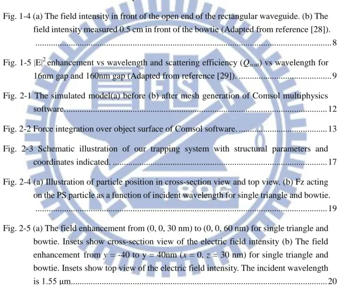
Furthermore, if there are two triangles forming small gap between their tips, field will be further enhanced in the gap. Sundaramurthy et al. [29] proved this by showing that field enhancement within 16 nm gap is 5 times stronger than that within 160 nm gap (Fig. 1-5).
9
Fig. 1-5 |E|2 enhancement vs wavelength and scattering efficiency (Qscat) vs wavelength for 16nm gap and 160nm
gap (Adapted from reference [29]).
Compared to regular metallic structure, bowtie with lightning-rod effect and gap effect produce sub-diffraction confinement and large enhancement of the incident optical intensity. These results altogether generate sharp intensity gradient of the near-field which yields greatly amplified optical forces.
10
1-3 Motivation
In this study, we use gold bowtie structure as a plasmonic tweezers, because it can concentrate the field in the central gap, and can exhibit remarkable field enhancement. In trapping application, the highly concentrated and enhanced field can generate very strong optical forces and can trap particles down to nanometer scale with very small trapping site. That means the trapping would be very efficient and accurate. These features can only be attained by plasmonic tweezers with tip and gap structure together. Furthermore, we integrate the gold bowtie structure with optical waveguide to enhance excitation efficiency. In the contrary, conventional ways such as coupling directly from the top or using prism scheme are not efficient because most of the incident light in these configurations is transmitted without interacting with the plasmonic structure. To our knowledge, the integration had not been proposed before. And it will be a very compact system with both particle manipulation unit and excitation route in a chip.
11
Chapter. 2
Structure design and numerical characterization
2-1 Optical force analysis
In order to understand the behavior of particle affected by LSPR around the bowtie, we calculate the optical forces acting on the particle. Approximations and numerical analysis are used according to the particle size. Mie’s scattering theory, which can be understood by sense of ray optics and Newton’s third law, has been widely used in many researches of conventional optical tweezers. However, it is only for large particles. Tiny biological particles are always out of its scope. Rayleigh scattering theory is right for calculating optical forces on very tiny particles with size much smaller than the incident wavelength. But it is still not suitable for analyzing forces on the particle in our case. This is because the field is highly concentrated with distribution comparable to the particle size. As a result the particle cannot be regarded as a point dipole in vicinity of the LSPR without affection on the field as required in Rayleigh approximation. Finally only Maxwell stress tensor is suitable for rigorously analyzing our case. Here we expended the time averaged force density in Cartesian coordinate (in x, y, and z direction): )) B ( ) H real(conj( z + )) (D ) E real(conj( z + )) B ( ) H real(conj( y + )) (D ) E real(conj( y + )) B ( ) H conj( + ) B ( ) conj(H + ) (B ) H (conj( x 2 1 -) D ( ) E conj( + ) D ( ) E conj( + ) (D ) E (conj( x 2 1 -)) B ( ) H real(conj( x + )) (D ) E real(conj( x Radius) 2(Particle 1 = > T < x z x z x y x y z z y y x x z z y y x x x x x x Mx (2.1)
12 )) (B ) H real(conj( z )) (D ) E real(conj( z + )) (B ) conj(H ) (B ) conj(H + ) (B ) (conj(H y 2 1 -)) (D ) conj(E ) (D ) conj(E + ) (D ) (conj(E y 2 1 -)) (B ) H real(conj( y + ) (D ) E real(conj( y -)) (B ) H real(conj( x + )) (D ) E real(conj( x Radius) 2(Particle 1 = > T < y z y z z z y y x x z z y y x x y y y y y x y x My (2.2) )) (B ) conj(H + ) (B ) conj(H + )) (B ) (conj(H z 2 1 -)) (D ) conj(E + ) (D ) conj(E + )) (D ) (conj(E z 2 1 -)) (B ) H real(conj( y + )) (D ) E real(conj( z + ) (B ) H real(conj( y + ) (D ) E real(conj( y -)) (B ) H real(conj( x + )) (D ) E real(conj( x Radius) 2(Particle 1 = > T < z z y y x x z z y y x x z z z z z y z y z x z x Mz (2.3)
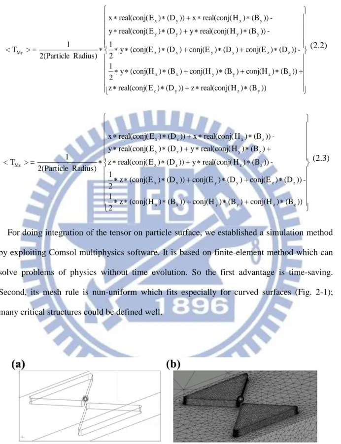
For doing integration of the tensor on particle surface, we established a simulation method by exploiting Comsol multiphysics software. It is based on finite-element method which can solve problems of physics without time evolution. So the first advantage is time-saving. Second, its mesh rule is nun-uniform which fits especially for curved surfaces (Fig. 2-1); many critical structures could be defined well.
13
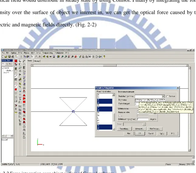
Besides, the mesh of each part can be defined individually depending on its importance. So we can largely save computer memories for calculation, and get the simulation results quickly. Finally its capability in post processing is almost impeccable. By which we can calculate the optical forces exerting on a particle easily. In our simulation we first build the bowtie we design, and put the target object at the position we interest in. Then we launch waves and simulate how optical field would distribute in steady state by using Comsol. Finally by integrating the force density over the surface of object we interest in, we can get the optical force caused by the electric and magnetic fields directly. (Fig. 2-2)
Fig. 2-2 Force integration over object surface of Comsol software.
From the force analysis, we were able to extract a parameter commonly used to describe stability of the trapping site: trapping potential U which is defined as [30][31]
rF r dr
U ( ') ' (2.4) It is the integration of the gradient force with respect to the position of particle perturbation
14
around the equilibrium point. The rule of thumb, established by Ashkin in his pioneering work, states that stable trapping requires a potential depth over 10 kBT to compensate for
stochastic kicks in the particle’s Brownian motion. However, potential in optical traps are rarely measured directly, the probability for the displacement of a trapped object in a potential well is first determined, then used in conjunction with the thermal energy kBT and given by a
Boltzmann distribution ( ) e x p ( ( )) e x p ( ) 2 T k r T k r U r P B B (2.5) when the potential is harmonic, the distribution is a simple parabolic parameterized by the trap stiffness α. Trap stiffness is also defined as
e q u i l i b r i um r F ) ( (2.6) it is the derivative of the restoring force with respect to the position of particle perturbed around the equilibrium point. The stiffness is also a parameter commonly used to evaluate optical traps. It can be regarded as elastic constants in mechanical system. Intuitively, the higher the stiffness means the tighter the trapped system.
15
2-2
Finite Element Method
In our work, wave propagation along the waveguide and finally interacting with the particle is simulated by COMSOL Multiphysics software based on finite element method (FEM). The method is a numerical technique for finding solutions of partial differential equations (PDE). For complicated optical systems, it can solve the boundary value problem, eigenvalue problem and find the steady state solution of a system by employing variational method. To apply this method, it requires discretizing a continuous domain into a set of discrete sub-domains, usually called elements, and the solution of each element would be approximated by certain characteristic form to solve the problems.
Here, the wave equations in the frequency domain for the magnetic and the electric fields are ( ( ) ( )) 2 ( ) 2 1 r H c r H r (2.7) ( ( ) ( )) 2 ( )) 2 1 r E c r E r (2.8) where c is the vacuum speed of light. To solve the wave equation for either magnetic or the electric field in frequency domain together with boundary conditions, standard FEM method proceeds in three steps. First, the wave equations are identified as solutions of certain variational problems where boundary condition at the surface has been incorporated as additional terms of lagrangian L. The most general variational formulation for the electric field is given by
V E E c E E dr E L [1( ) ( ) ] 2 1 ) ( 2 2 3
V V J E dr c i U E E n E n S d 3 0 0 ] ) ( ) ( 2 [ (2.9) where is the magnetic permeability and is dielectric function both may varied in space.16
In addition, denotes the outward normal at the surface and the electric field has to satisfy the Dirchlet boundary condition (nE)0 on S . and U are known quantities which are used to represent various other types of boundary conditions such as impedance boundary conditions and Sommerfeld radiation conditions. Finally, radiation sources within the computational domain V are described through the spatially varying current density J.
The second step is the most demanding step which consists of the discretization of the Lagrangian. The computational domain V is divided into a number of small-volume elements, the so-called finite elementary functions with unknown coefficients. It becomes possible to approximately enforce the div-conditions of the electric field within a field element as long as the dielectric function does not vary within this element.
In the final step, these expansions facilitate the transformation of the Lagrangian into a set of linear equations by Galerkin method [32]. This matrix system can subsequently be solved via advanced linear algebra methods, either for obtaining eigenfrequencies and eigennodes of the system of interest or to determine scattering cross sections of complex structure as well as transmittance and reflectance through functional elements.
17
2-3 Gold bowtie structure design for particle trapping
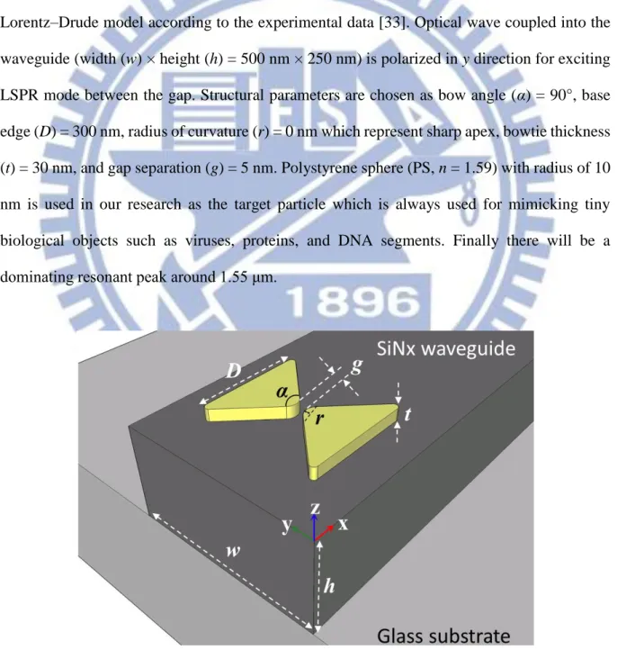
Fig. 2-3 illustrates the model design and computational domain used in this study. Here the bowtie structure is composed of two tip-to-tip isosceles triangles on silicon nitride waveguide (refractive index n = 2.2) fabricated on glass substrate (n = 1.45). Between the triangles, there is an accessible nanometric gap. Environment surrounding the system is assumed to be water (n = 1.33). In Fig. 2-3, the coordinate origin is actually located at the gap center on waveguide surface. The bowtie structure is made of gold whose dielectric constant is fitted by Lorentz–Drude model according to the experimental data [33]. Optical wave coupled into the waveguide (width (w) × height (h) = 500 nm × 250 nm) is polarized in y direction for exciting LSPR mode between the gap. Structural parameters are chosen as bow angle (α) = 90°, base edge (D) = 300 nm, radius of curvature (r) = 0 nm which represent sharp apex, bowtie thickness (t) = 30 nm, and gap separation (g) = 5 nm. Polystyrene sphere (PS, n = 1.59) with radius of 10 nm is used in our research as the target particle which is always used for mimicking tiny biological objects such as viruses, proteins, and DNA segments. Finally there will be a dominating resonant peak around 1.55 μm.
18
To determine the force exerted on a particle, a virtual spherical surface which enclosed the entire particle was used for calculation. In this work, 1W input power is launched as initial condition. The waves were launched into these waveguides with calculated boundary mode without insertion loss. By integrating Maxwell stress tensor over the surface enclosing the particle, we are able to obtain the optical forces exerting on the particle [34].
2-3-1 Enhancement provided by gap structure
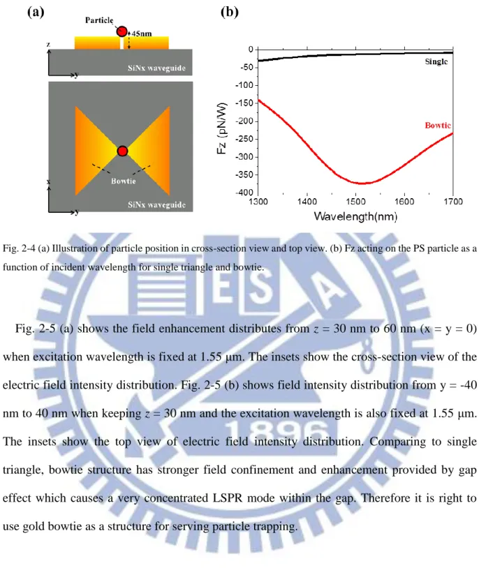
In order to investigate the dependence of optical force on LSPR mode in the gap, we vary the structural parameters and compare forces acting on it. The PS particle in these simulations is located at coordinate of (0, 0, 45 nm) (Fig. 2-4 (a)). For lower z positions, the surface will touch the bowtie causing an impractical situation with overlap of particle and the bowtie. So the nearest position we select is at z = 45 nm. For comparison we also simulate the reference case with one triangle of the bowtie eliminated. Results corresponding to this reference case are noted by “single”. Red curve in Fig. 2-4 (b) shows the spectral response of vertical optical force Fz exerted upon the PS as a function of wavelength when it is trapped by LSPR mode of the bowtie structure. In the figure, negative sign of Fz is consistent with the trapping nature along -z direction. One can see that Fz becomes stronger significantly when wavelength gets closer to resonance near 1.55 μm. The PS particle will experience maximum vertical force as strong as 362 pN under 1 W excitation. Comparing to the reference case as shown by black curve in Fig. 2-4 (b), that force is over thirty times larger and is also much stronger than that achieved in reference [28].
19
Fig. 2-4 (a) Illustration of particle position in cross-section view and top view. (b) Fz acting on the PS particle as a function of incident wavelength for single triangle and bowtie.
Fig. 2-5 (a) shows the field enhancement distributes from z = 30 nm to 60 nm (x = y = 0) when excitation wavelength is fixed at 1.55 μm. The insets show the cross-section view of the electric field intensity distribution. Fig. 2-5 (b) shows field intensity distribution from y = -40 nm to 40 nm when keeping z = 30 nm and the excitation wavelength is also fixed at 1.55 μm. The insets show the top view of electric field intensity distribution. Comparing to single triangle, bowtie structure has stronger field confinement and enhancement provided by gap effect which causes a very concentrated LSPR mode within the gap. Therefore it is right to use gold bowtie as a structure for serving particle trapping.
20
Fig. 2-5 (a) The field enhancement from (0, 0, 30 nm) to (0, 0, 60 nm) for single triangle and bowtie. Insets show cross-section view of the electric field intensity (b) The field enhancement from y = -40 to y = 40nm (x = 0, z = 30 nm) for single triangle and bowtie. Insets show top view of the electric field intensity. The incident wavelength is 1.55 μm.
To examine the spatial distribution of the trapping force, we fix the wavelength at 1.55 μm and move the PS particle along z axis (x = y = 0) as shown in Fig. 2-6 (a). Obviously, the force will become stronger when the PS particle gets closer to the gold bowtie. And the force will die out fast when it moves few tens of nanometers away. This is the evanescent characteristic of near-field optical trapping. Therefore only neighboring particles will be trapped. This characteristic will provide selectivity for trapping in microfluidic systems.
21
Fig. 2-6 (a) Fz acting on the PS particle as a function of position along the z axis (x = y = 0). (b) Fx as a function of location along the axis of (x, 0, 45 nm) (indicated by red arrows in top-view schematic). (c) Fy as a function of position along the axis of (0, y, 45 nm) (indicated by green arrows in top-view schematic).
The other two paths are along x and y directions when z = 45 nm as indicated by red and green arrows in the insets of Fig. 2-6 (b) and (c), respectively. The evolution of Fx and Fy as functions of location along x and y directions are shown in Fig. 2-6 (b) and (c), respectively. We see that Fx (Fy) is positive when the particle is at x (y) < 0 and is negative when it is at x (y) > 0. This is the trapping nature. Finally the particle will be trapped at x (y) = 0 nm (equilibrium position), where it will experience no optical force in x (y) directions. In other words, Fx (Fy) changes sign when the PS particle moves across center of the bowtie. This means that naturally the PS particle will be driven toward the center as it falls into the trapping zone. Notably, Fx has maximum force 46 pN/W at x = 11 nm and the maximun for Fy is 50 pN/W at y = 11 nm. And we obtained a theoretical stiffness of 4.35 pN/ (nm•W)
22
along x direction and 4.96 pN/(nm•W) along y direction. This is because the field is more concentrated along y direction than x direction. Finally, the resultant effect of Fx, Fy, and Fz will produce a stable trapping site near the gap.
Actually LSPR mode of the bowtie not only can trap particles on top of the gap but also can trap particle from either side of the gap. Fig. 2-7 (a) illustrates the possible trapping position when the particle is nearest to side of the gap. We show the horizontal force acting on particle along x direction when z = 15 nm as shown in Fig. 2-7 (b). The dash line represents the region in which the particle cannot approach because of size limitation. We see that Fx is positive when the particle is at x < 0 and is negative when it is at x > 0. The Fx will attract the particle getting closer to the gap and finally the particle will be stuck at either side of the gap. Maximum horizontal force the particle will experience is 1389 pN/W. This force is three times higher than that when the particle is trapped on the top of gap. Therefore the trapping is not limited from the top.
Fig. 2-7 (a) Illustration of particle position in cross-section view and top view.(b) Fx acting on the PS particle as a function of location along the axis of (x, 0, 15 nm). The position in which particle can’t enter is fitting by dash line.
23
Fig. 2-8 plots the potential distributions in the three directions corresponding to Fig. 2-7. The potential is calculated by integrating parallel component of the trapping force along the path in each direction. Here the zero potential point is set at position 2 μm far from the bowtie gap center because field distribution decays exponentially to negligible there. The highly concentrated field distribution and resonant enhancement leads to a depth of the trapping potential much larger 10 kBT even for particles with sizes down to 20 nm. Since trapping
force on the particle at sides of the gap is much stronger than that at top center of the gap, it can be predicted that the potential depth at sides of the gap must also be larger than 10 kBT.
That means the particle coming from any direction can be trapped stably around the gap without being disturbed by Brownian motion.
24
2-3-2 Dependence on gap size
To further realize the coupling effect between single triangles on bowtie, we calculate vertical force depending on different gap size from 5 nm to 90 nm as show in Fig. 2-9 (a). In this investigation the particle is at coordinate of (0, 0, 50 nm). For comparison, the peak wavelength and force in each gap size are summarized in the Fig. 2-9 (b) and (c).
Fig. 2-9 (a) Simulated spectra of Fz exerted upon the particle trapped by the bowtie structure with gap size varied from 5 nm to 90 nm, r = 0, D = 300 nm, t = 30 nm, and α = 90°. (b) Summarizing peak wavelength with gap size. (c) Summarizing peak force Fz with gap size.
25
We find the peak of Fz exponential decreases and blueshifts as the gap size reduces. To explain this phenomenon, we plot electric field intensity under different gap size at each resonance peak as show in Fig. 2-10. For gap smaller than 50 nm, the surface charge is confined to a small fraction of the total bowtie area and there is a strong displacement current flowing in the gap between the triangles. Consequently, plasmon resonance of the coupled structure is strongly controlled by dipole mode across two triangles with field in the y direction. For gap larger than 50 nm, the surface charges tend to distribute individually in each triangle. Since the coupling effect between the two triangles is small, peak resonance would fix near 1.3 μm and the field distribution approaches that of a single triangle when gap size becomes larger. Therefore for utilizing gap effect to enhance the trapping forces, the gap must be smaller than 50 nm.
Fig. 2-10 The top view of electric field intensity for (a) gap size=5 nm, λ=1.55 μm. (b) gap size=30 nm, λ=1.4 μm. (c) gap size=60 nm, λ=1.33 μm. (d) gap size=90 nm, λ=1.3 μm.
26
2-3-3 Consideration for fabrication
Despite bowtie has great optical force and potential, the established condition is for perfectly sharp apexes of bowtie with gap size as small as 5 nm in simulation. To take the limit of fabrication into consideration, we simulate the dependence of optical force on attainable bowtie geometry in experiment.
Fig. 2-11 (a) shows the dependence of optical force on radius of curvature (ROC) of the bowtie central apexes. The particle is at coordinate of (0, 0, 50 nm). This investigation is for practical consideration because it is easier to fabricate obtuse apexes instead of sharp ones. We vary the ROC from zero (perfect sharp tips) to 50 nm while keeping gap separation of 5 nm. For comparison, the peak wavelength and force in each ROC are summarized in the Fig. 2-11 (b) and (c). When the ROC is small, there exists certain mode mismatch between the coupling waveguide and the bowtie. Only parts of the waveguide mode will interact with the bowtie. When ROC increases gradually, one can see that the peak optical force becomes stronger and the wavelength redshifts slightly. When ROC = 10 nm, the coupling between the waveguide mode and the LSPR mode will become optimized and is most efficient. In this condition the force will reach its maximum near 1600 nm. Further increasing the ROC makes the modes become mismatch again. Besides, when the apexes become more obtuse, the lightening-rod effect will diminish. Therefore the electric field would no longer concentrate at tips and peak force reduces much faster.
27
Fig. 2-11 (a) Simulated spectra of Fz exerted upon the particle trapped by the bowtie structure with r varied from 5 to 50 nm, α = 90°, D = 300 nm, t = 30 nm, and g = 5 nm. (b) Summarizing peak wavelength with ROC. (c) Summarizing peak force Fz with ROC.
Another consideration is about fabrication error of gap size. Actually the 5 nm gap is not easy to be fabricated precisely. Even error of a few nanometers would change a great fraction in such small gap size. Therefore we prefer to increase gap size to 30 nm for reducing the effect of fabrication error. However, the peak wavelength of optical force would blueshift when gap size increases. For retaining the resonance peak at 1.55 μm, we simulate the dependence of peak force on base edge (D) of the bowtie while keeping 90° bowtie angle and taking 10 nm ROC as show in Fig. 2-12. In this investigation the particle is still at coordinate
28
of (0, 0, 50 nm). When D = 350 nm, the plasmon resonance has a maximum optical force Fz at 1.55 μm. Finally, our structure parameter in experiment would be α = 90°, D = 350 nm, ROC = 10 nm, t = 30 nm, and g = 30 nm.
Fig. 2-12 Simulated spectra of Fz exerted upon the particle trapped by the bowtie structure with D varied from 300 to 350 nm, α = 90°, r = 10 nm, t = 30 nm, and g = 30 nm.
In this condition, we show the spatial distribution of the trapping force when moving the PS along z axis (x = y = 0) at wavelength of 1.55 μm as shown in Fig. 2-13 (a). For g = 30 nm, the PS of 20 nm diameter can enter in gap, and the lowest z position is z = 15 nm. The negative optical force Fz will attract the PS into the gap and the maximum force experienced by the particle will be 158 pN/W when it is at z = 35 nm. The other path is along x direction when z = 15 nm (the PS is in the plane at vertical center of the bowtie). The variations of Fx as a function of position along x direction is shown in Fig. 2-13 (b). In this case, the particle will be clipped by bowtie along y direction. We see that Fx has maximum force 165 pN/W at
x = 10 and -10 nm. The theoretical trapping stiffness in this direction is 19.3 pN/nm/W. The
29
Then the particle cannot move in y direction because the two apexs limit freedom of the particle in y direction and finally it will be trapped at (0, 0, 15 nm). We also calculate the trapping potential along z and x axis as shown in insets of Fig. 2-13 (c), and (d). They show the PS will be trapped stably by LSPR mode of the bowtie structure in the central gap.
Fig. 2-13 (a) Fz acting on the PS particle as a function of position along the z axis (x = y = 0). (b) Fx as a function of location along the axis of (x, 0, 15 nm) (indicated by red arrows in top-view schematic). (c) Potential along z axis by integrated the trapping force Fz. (d) Potential along x axis by integrated the trapping force Fx.
In order to know the trapping ability for particle of different size, we investigate the dependence of vertical trapping force on PS of diameter ranging from 20 to 1000 nm (Fig. 2-14). We keep the closest position of particle on the top of bowtie when particle diameter increases. We see that the Fz will significantly increase when the particle size increases. The force experienced by the particle will be as strong as 2773 pN/W when particle diameter is 500 nm. Particle size induce negligible peak wavelength shift because the gap mode is highly
30
concentrated in the gap (Fig. 2-15).
Fig.2-14 (a) Simulated spectra of Fz exerted upon the particle trapped by the bowtie structure with particle diameter varied from 20 to 1000 nm, α = 90°, r = 10 nm, D = 350 nm, t = 30 nm, and g = 30 nm. (b) Summarizing peak wavelength with particle diameter. (c) Summarizing peak force Fz with particle diameter.
31
Fig.2-15 The side view of electric field intensity for 500 nm PS. Inset shows electric field intensity zooming out along x direction.
2-4 Summary
In this section, we use finite element method to simulate wave propagation along the waveguide and coupled into LSPR mode of the gold bowtie structure for interacting with nanometric particles. For 20 nm PS trapped by bowtie of sharp apexes with 5 nm gap, the maximum trapping force in z direction will be 362 pN/W. And the trapping phenomenon is not only happening on top of the gap. For the PS coming from either side of the gap, the trapping force in x direction would be as strong as 1389 pN/W. However for fabrication consideration, a structure with gap of 30 nm and 10 nm ROC of the apexes is more feasible. When trapping by the bowtie with these parameters, the trapping forces for PS of 20 nm will be Fz = 158 pN/W with potential depth over 100 kBT. Therefore the PS will still be trapped
32
Chapter. 3
Fabrication and measurement
3-1 Fabrication process
Gold bowtie is made on silicon nitride waveguide based on glass substrate. At first, silicon nitride film is deposited on glass substrate by using plasma-enhanced chemical vapor deposition (PECVD) at temperature of 200°. The film thickness is 300 nm. Then a 240 nm polymethyl methacrylate (PMMA) layer is spun on the sample by using spin coater. The waveguide pattern is defined on the PMMA layer by using electron beam lithography (EBL). And the waveguide defined on PMMA is transferred to silicon nitride layer by using reactive ion etching (RIE). The residual PMMA layer can be removed by acetone (ACE). This process flow for fabricating the silicon nitride waveguide is illustrated in Fig. 3-1.
33
For making gold bowtie structure, PMMA layer is spun on the sample again followed by a conducting layer (ESPACER). This layer can solve the problem of charge accumulation which will make the resultant pattern distorted in EBL process. The pattern for the bowtie is also written by using EBL on PMMA. During the exposure step, we use predefine marks to do alignment process, by which the bowtie pattern can be written right on the waveguide. Actually there is a standard deviation of about 3 μm in alignment process. Therefore we have to make an array of the bowtie to compensate the deviation. After the exposure, the ESPACER layer can be removed by DI water rinsing. Au layer of 30 nm thickness is then deposited at a rate of 0.4 Å /s by thermal evaporation. Then, the PMMA resist and the overlaying Au layer with PMMA underneath can be removed by lift-off process. This is a process conducted conveniently by immersing the sample in ACE at room temperature for 4 hours. Finally there is only bowtie structure laid on the waveguide with no PMMA remaining. Whole this part of process flow is illustrated in Fig. 3-2.
Fig. 3-2 The second part of fabrication process.
34
The above process is implemented from bottom to top. It is intuitive that we make the waveguide first and then put the bowtie on it. However after the waveguide is completed it becomes much easier for the electron to accumulate on the sample surface. And the resultant pattern in EBL process will be distorted severely. Therefore the bowtie fabricated in this process has no sharp apexes as we expect (Fig. 3-3 (a)). In the contrary, we can also reverse the process to do it from top to bottom. That is fabricating the gold bowtie, by EBL and lift-off process, on an intact silicon nitride film first. And then a PMMA layer is spun on the sample followed by EBL and RIE etching to define silicon nitride waveguide on the substrate. This reverse process has several advantages. First, charges can be grounded by the intact silicon nitride film and thus the bowtie can be made with clear shape as what we design without distortion. Fig. 3-3 (b) shows SEM picture of the fabricated device by using the reverse process. It is obvious that the apexes are sharper than that fabricated by using normal process. Second, we can choose bowtie of appropriate parameters and fabricate waveguide structure underneath it. That will increase workability of the fabricated sample.
Fig. 3-3 The top view SEM pictures of these structure (a) general process (b) reverse process.
We check surface roughness and thickness of the gold bowtie by atomic force microscope (AFM) and P-10 surface profiler. Fig. 3-4 (a) shows top view AFM picture of the bowtie array
35
and white line indicates the cross section view we take as shown in Fig. 3-4 (c). Vertical distances between positions indicated by the red triangles and by the green triangles are measured respectively. We can see the measured thickness of bowtie is very close to 30 nm as what we expect and RMS of surface roughness is very low as only 2.37 nm. The profile shown in Fig. 3-4 (a) seems no gap is there between the two triangles. The gap cannot be resolved by AFM measurement because the picture composes only 256 lines and the line resolution is 7.81 nm. For clarification, we show the SEM picture of the same bowtie array to confirm that the geometry is what we design (Fig. 3-4 (b)). For P-10 surface profiler measurement, we prepare a test sample with a tape sticks on it as mask. Then the tape is removed from the sample surface after Au film deposition. Then we measure the height difference between the region with Au film and the region of bare substrate to get thickness of the film. The average thickness of Au film among four test samples is 30.2 nm.
Fig. 3-4 (a) Top view AFM picture. (b)Top view SEM picture. (c)Line cross section AFM picture (white line in Fig.3-4(a)).
36
After we finish the above fabrication process, it is necessary to make an entrance for coupling light at one end of the waveguide. Generally, we used to cleave the sample to make the waveguide entrance show up at edge of the sample. But there are a lot of difficulties for cleaving the glass substrate because there is no crystallographic orientation on it, and it is too hard to be cleaved. So we use a process of mechanical grinding and polish to make the waveguide entrance appear for light coupling. The grinding sheet is classified by its roughness. The sheet of lower number is rougher and the sheet of higher number is finer. We use sheet of 80 to initiate the process. It can make the sample edge close to end of the waveguide quickly. Then we use sheets finer by finer to make the waveguide end appear progressively and remove the damaged region. Finally we use sheet of 4000 to polish the edge for better coupling.
37
3-2 Experimental setup
Fig. 3-5 shows the schematic illustration and real picture of the measurement configuration which is set up to be an upright system because we have to contain particles in water in the following observation. Light from a halogen lamp serves image lighting and provides continuous spectrum for analysis. The light first passes through an iris which can control the diameter of the spot in image plane. Then the light passes through a pellicle beam splitter (BS) deviated with 45 degree from the vertical axis. The BS is used only for guiding the reflected light from the sample to CCD camera. And it will be flipped out of the optical axis when doing spectrum analysis. Next the light will be focused by a 20X objective lens on the sample surface. The waveguide, bowtie, and particles are lighted up by the incident light. The reflected light will be collected by the same objective lens and reflected by beam splitter and mirror to the CCD camera. Finally the image can be observed on a monitor. For exciting LSPR mode of the bowtie structure on waveguide, we use a laser as source which is given by HP 8168 tunable laser with erbium doped fiber amplifier. The tunable range is from 1480 nm to 1580 nm. The laser is injected into the waveguide through a fiber with taper and lens tip, which and the sample are immersed in water together. We tune the laser to wavelength of 1550 nm to do the measurement. The output power measured at the tapered fiber end is 60.2 mW.
38
Fig. 3-5 (a) Configuration and (b) photography of upright image system
Fig. 3-6 shows schematic illustration of a thin fluidic chamber used in our experiment. It is 0.125 mm thick composed of cover slip and short fiber sections as spacers. The cover slip adheres on the sample surface by capillary effect. The chamber contains the PSs dispersed in de-ionized water. And the whole sample is immersed water surrounding. In our experiment we use polystyrene micro-spheres of 1 μm diameter (standard deviation is claimed to be smaller than 0.01%) instead of 20 nm ones as that used in our simulation. That is because of the diffraction limit which makes it is really difficult to observe such tiny particles even by using system of very high resolution. But we still can demonstrate the transportation and trapping ability of the system we design by using PS of 1 μm diameter. The particles are suspended in de-ionized water with 1% Triton X-100 non-ionic surfactant to prevent aggregation of the nanoparticles and to minimize adhesion between micro-particles and the surface of the devices. Finally if the particle is stuck on the bowtie, it must be the optical forces trapping the particle.
39 Fig. 3-6 The schematic diagram of the thin chamber.
3-3 Spectral analysis
Before doing trapping experiment, we measure transmission spectrum of the bowtie array and calculate corresponding extinction spectrum of the LSPR mode to ensure that the bowties we fabricated is exactly what we design in simulation works. The resultant extinction spectra are show in Fig. 3-7 (a). The excitation is polarized in y direction crossing gap of the bowties and the dipole mode and quadruped mode resonates at 1060 nm and 740 nm, respectively(Fig. 3-7 (b)(c)). The sample is fabricated with gold bowtie array on glass substrate. The array is two dimensional with period of 1 μm. We use halogen lamp as the source passing through a polarizer. Finally, the polarized light along y direction illuminates to the sample. We analyze transmission signal by optical spectrum analyzer (OSA). The transmission extinction is defined as - log (E1 / E0), which represents the response of the bowtie array to the incidence. Here, E1
indicates transmitted power passing through the sample with bowtie array, while E0 indicates
40
picture of the fabricated bowtie array. One can see that the experiment λmax and simulation λmax
are close at 1083 nm and 1060 nm, respectively. The small inconsistence in wavelength may be coming from two fabrication imperfection. One is the inevitable error in dimension. Second is the randomly missed triangle in a bowtie. In Fig. 3-8, we show the extinction spectra of bowtie array on glass substrate with gap size varied from 0 nm to 85 nm. When the gap size = 0 nm (two apex stick to each other), there is no obvious signal in extinction spectrum. The peak wavelength will blue-shift when gap size increases. For further increase, the amount of shift will saturate because the case will converge to array of single triangles with no coupling in between. This tendency is consistent with the simulation result.
Fig. 3-7 (a)The extinction spectral of bowtie array on glass substrate with incident light polarize along y direction. Inset shows SEM picture of bowtie array. (b) The top view of surface change distribution for λ=0.74 μm. (c) The top view of surface change distribution for λ=1.06 μm.
41
Fig. 3-8 (a) The extinction spectral of bowtie array with gap size varied from 0 nm to 85nm on glass substrate (b) Summarizing peak wavelength with gap size.
In addition, because the resonance wavelength is very sensitive to the bowtie geometry, we compare the bowtie parameters (measured by SEM) used in this experiment with that used in our theoretical work (Table. 3-1). It is obvious that the fabrication is controlled very well that the parameters are very similar to those designed in simulation work. Therefore we can say that the fabricated bowties are what we designed. And the resonance is the LSPR mode we want with strong field in the gap.
Table. 3-1 Experiment and theoretical geometric parameters of bowtie.
Angle (α) Base edge (D) ROC (r) Thickness (t) Gap (g) Experiment 90.3 343.2 nm 9.4 nm 30.2 nm 29 nm Theoretical 90 350 nm 10 nm 30 nm 30 nm
42
3-4 Demonstration of trapping
The particle transportation and trapping ability are measured at about 200 μm away from the input ports of the waveguide. Fig. 3-9 shows the 1 μm particle move as time evolves on a 0.8 μm wide waveguide when the continuous wave laser source operated at 1.55 μm is coupled into the waveguide. From t = 20 s to 80 s, the radiation pressure induced by the evanescent field of the guided mode tends to push the particle along the waveguide toward the trapping region of bowtie. At t = 80 s, the particle stop moving at the position where bowtie is located (indicated by orange dash line). From t = 80 s to 140 s, the particle stop on the bowtie stably no matter that the radiation pressure still push it forward. Meanwhile there are some particles moved by the scattering light not coupled into the waveguide near the stably trapped one. That means the stop one is really trapped by the bowtie. This trapping phenomenon lasts for 1 min. And it can actually last for longer if we keep the laser on. When we turn off the laser after t = 140 s, the particle moved very fast away from the trapping bowtie. Therefore we reduce the time step to 10 s to trace motion of the particle. The quick escape is caused by Brownian perturbation when no LSPR mode can serve trapping anymore. Whole this process demonstrates transportation and trapping of the particle was really caused by optical forces rather than nonspecific binding. It is obvious that in period of t = 20 s to 80 s, the particle is on top of the central axis of the waveguide. However when it is trapped by the bowtie, it is deviated from the central axis. This can be explained by SEM picture of the used bowtie as shown in Fig. 3-10. The bowtie is actually laid near one side of the waveguide. That is why the trapped particle is not on top of central axis of the waveguide. And that is another evidence of the trapping ability provided by the bowtie.
In our observation, only the particles transported along the waveguide has the chance to be trapped by the bowtie. Particles swimming around the bowtie are not observed to be trapped. This can be explained by the highly concentrated LSPR mode both in transverse and vertical
43
directions. Only particles very close to the bowtie have the chance to be trapped. This feature is consistent with the simulation result that the optical forces only extend a few hundred nanometers around the central gap. On the other hand, the coupling waveguide not only transports particle but also increases probability of particle trapping.
Fig. 3-9 Motion of 1 μm particle (indicated by black arrows) as time evolves on 1 μm wide waveguide in 1.55 μm wavelength and bowtie position indicated by dash line.


![Fig. 1-1 Ray optics description of the gradient force (Adapted from reference [1]).](https://thumb-ap.123doks.com/thumbv2/9libinfo/8709674.199915/14.892.144.765.307.919/fig-ray-optics-description-gradient-force-adapted-reference.webp)
![Fig. 1-2 Schematic illustration of (a) slot waveguide (b) nanoslot waveguide photonic crystal cavity (Adapted from reference [24][25])](https://thumb-ap.123doks.com/thumbv2/9libinfo/8709674.199915/18.892.160.782.109.339/schematic-illustration-waveguide-nanoslot-waveguide-photonic-adapted-reference.webp)
![Fig. 1-5 |E| 2 enhancement vs wavelength and scattering efficiency (Q scat ) vs wavelength for 16nm gap and 160nm gap (Adapted from reference [29])](https://thumb-ap.123doks.com/thumbv2/9libinfo/8709674.199915/20.892.157.769.115.342/fig-enhancement-wavelength-scattering-efficiency-wavelength-adapted-reference.webp)