Broadband Tapered Microstrip Leaky-Wave Antenna
Wanchu Hong, Tai-Lee Chen, Chi-Yang Chang, Jyh-Wen Sheen, and Yu-De Lin
Abstract—This study proposes a novel scheme based on the characteristics of leaky-wave antennas for the empirical design of broadband tapered microstrip leaky-wave antennas. This scheme can explain and approximately model the radiation characteristics of a linearly tapered leaky-wave microstrip antenna. A broadband feeding structure that uses the balanced and the inverted balanced microstrip lines to form a pair of broadband baluns is also presented. The measured return loss of the inverted balanced microstrip lines has a VSWR 2 from dc to 18.6 GHz and that of the back-to-back feeding structures has aVSWR 2 from 2.2 to 18.6 GHz. This feeding structure can be used to feed a broadband planar leaky-wave antenna with a fixed mainbeam that uses the tapered microstrip structure. The measured bandwidth of the antenna for aVSWR 2 exceeds 2.3:1.
Index Terms—Broadband planar balun, feeding structure, leaky-wave, microstrip, tapered antenna.
I. INTRODUCTION
A
CCORDING to the characteristics of space-wave leakage of higher order modes on planar transmission lines [1]–[4], the radiation bandwidth of microstrip leaky-wave antennas exceeds that of planar resonant antennas, such as patches and printed dipoles. And because of their simplicity of fabrication, the microstrip leaky-wave antennas are very appropriate for millimeter-wave applications [5]. The mi-crostrip leaky-wave antennas have different applications, such as frequency-scanning antenna [6], point-to-point high-gain antenna [7], multibeam antenna [8], and active integrated antenna [9], according to the choice of the higher order modes, structural parameters and structure profiles. For the point-to-point communication, the mainbeam variation caused by the frequency-scanning feature of leaky-wave antennas should be as low as possible. A direct and possible solution to the mainbeam-scanning problem is to use a tapered line structure so that radiation in different frequency regions uses different parts of the antenna, resulting in a fixed mainbeam. This structure is inherently broadband. This study presents such a broadband tapered antenna, based on the first higher order mode of the microstrip leaky-wave antennas with a fixed mainbeam. The radiation bandwidth of a microstrip leaky-wave antenna is generally less than 20%. The limitation of the bandwidth is dominated by the dielectric constant of theManuscript received January 18, 2001; revised May 30, 2002. This research was supported in part by the Ministry of Education for Advanced Technologies for Telecommunications (A) under Grant 90-E-FA06-2-4 and in part by the Na-tional Science Council under Grant NSC-90-2213-E-009-066.
W. Hong, C.-Y. Chang, and Y.-D. Lin are with the Institute of Communication Engineering, National Chiao Tung University, Hsinchu, Taiwan, R.O.C. (e-mail: [email protected]).
T.-L. Chen is with the Department of Physics, National Central University, Tao-Yuan, Taiwan, R.O.C.
J.-W. Sheen is with the Walsin Technology Corporation, Tao-Yuan, Taiwan, R.O.C.
Digital Object Identifier 10.1109/TAP.2003.814739
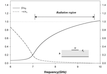
Fig. 1. Typical propagation characteristics of the normalized phase constant =k and the attenuation constant 0 =k of the microstrip leaky-wave first higher order mode (w = 13:58 mm, h = 0:508 mm, " = 2:2).
substrate and by the feeding structures. If the dielectric constant of the antenna substrate equals one, the radiation region of the microstrip higher order modes can cover the entire band above their cutoff frequency. However, the dielectric constant of the commonly used microwave substrate is about 2.2 and thus the radiation bandwidth is reduced. Adopting a tapered line struc-ture can also improve the bandwidth of the leaky-wave antenna [10], [11]. Here, a semi-synthetic design procedure is proposed for designing multisection antennas. This design procedure can also be applied as a stepped approximation method to explain and approximately model the tapered microstrip line with a linear profile. This method was widely used to analyze the tapered slot antenna [12]–[14].
The design of a broadband feeding structure is also es-sential to exploit fully the broadband feature of a tapered microstrip leaky-wave antenna. Some typical feeding struc-tures for exciting the first higher order mode of a microstrip leaky-wave antenna include unsymmetrical microstrip line [2], microstrip-to-slotline [15], coplanar waveguide (CPW)-to-slot-line [9], coaxial-to-microstrip [16], aperture-coupled [17], and microstrip-to-coplanar strips (CPS) [18]. The bandwidth of these feeding structures is not sufficiently wide (less than or around about 20%) for broadband applications. This study presents a broadband feeding structure that uses balanced [19] and inverted balanced microstrip lines to form a pair of broadband baluns. Using this broadband structure can realize a broadband leaky-wave antenna based on tapered microstrip lines.
II. DESIGN OF THETAPEREDMICROSTRIPLEAKY-WAVE ANTENNA
Fig. 1 shows typical propagation characteristics of the mi-crostrip first higher order leaky mode. These characteristics can 0018-926X/03$17.00 © 2003 IEEE
HONG et al.: BROADBAND TAPERED MICROSTRIP LEAKY-WAVE ANTENNA 1923
be obtained by full-wave analysis such as spectral domain anal-ysis (SDA) [4]. The radiation leaky region can be defined as the band between the frequency point at which the phase constant equals the attenuation constant , and that at which the phase constant equals the free-space wavenumber . The frequency region below the radiation region can be consid-ered as the reactive region owing to its evanescent property. At a frequency above the radiation region the bound mode
prop-agates because and (A very narrow frequency
region exists for surface-wave leakage, and is given by ) [4]. The cutoff frequency of the radiation region and the radiation bandwidth of the microstrip first higher order mode can be approximately estimated from the following equations, derived from the lossy waveguide model [20].
(1) (2) Here, is the speed of the light in a vacuum; is the effective line width, and is the dielectric constant. These equations show that the radiation bandwidth of a microstrip leaky-wave antenna is governed by the line width after the sub-strate is selected. As the microstrip width becomes narrower, the cutoff frequency increases and thus the radiation region will shift toward a higher frequency range. Using a tapered line of varying width enables the different but partially overlapped ra-diation regions to apply at different parts of the antenna when the operating frequency is increased. Notably, a microstrip an-tenna with narrower width radiates in the higher frequency re-gion but enters into the reactive rere-gion at a lower frequency, such that no power is passed or radiated. In contrast, the wider microstrip antenna radiates in the lower frequency region and enters into the bound mode region at a higher frequency, so that almost all the power is passed in the higher frequency re-gion. Consequently, the tapered microstrip antenna should be fed from its wide edge, as is clarified by a practical example in Section IV. A broadband antenna can be implemented by ar-ranging and connecting these microstrip sections in an appro-priate way, so that the union of the radiation regions of each mi-crostrip sections corresponds to the desired band. Such design methodology leads to the prototype of multisection microstrip antennas. However, the impedance mismatch and the disconti-nuity effect of this multisection microstrip antenna reduce the bandwidth and enhance the spurious sidelobes. Understanding the characteristic impedance of the microstrip first higher order mode, for example, by leaky-mode parameter extraction tech-nique [21], helps to solve the problem of impedance-matching. In this case, a lossy waveguide model [22] can be used to es-timate approximately the characteristic impedance of the mi-crostrip first higher order mode at the feeding point. The for-mula is given in [19] and repeated here for convenience:
(3) Where is the intrinsic impedance; is the complex propagation constant of the first higher order mode; is the
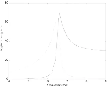
Fig. 2. Simulation results for the characteristic impedance of the microstrip first higher order mode from the lossy waveguide model. The solid lines are for the real part ofZ and the dashed lines are for the imaginary part. (w = 14:6 mm,h = 0:508 mm, " = 2:2).
free space wavenumber; is the distance from the center of the strip to the feeding point; is the effective line width, and is the thickness of the substrate. Fig. 2 presents the simula-tion results of a 14.6-mm wide microstrip line on a 0.508-mm thick substrate with a dielectric constant of 2.2. The charac-teristic impedance is less dispersive and approaches a constant when the operating frequency is increased. This property shows its usefulness in ultra-broadband applications. Equation (3) can help to select the appropriate antenna substrate to yield the de-sired range of antenna input impedance.
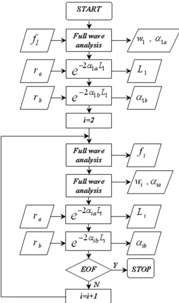
Another question concerns how to determine the width and length of each microstrip section, such that the power could be uniformly radiated at different frequencies. A possible solution is proposed here. If the bandwidth ranges from to , then the width of the first microstrip section, , can be deter-mined by setting the onset (or cutoff) frequency of the radiation region of this first microstrip section to . The sur-vival power ratio at the end of the strip can be estimated as ap-proximately , since the power distribution exponentially decays along the strip,. Two parameters need to be set before-hand. One is the estimated survival power ratio
(4) at the end of the section at frequency . The other is the esti-mated survival power ratio
(5) at the end of the same section at frequency which is as-signed as the onset leakage frequency of the next microstrip section. The above equations yield the length of the sec-tion and the attenuation constant at the reactive frequency of the subsequent section. Then, the frequency , where the attenuation constant equals to for this same section, can also be found. Now, the width of the subsequent microstrip section, , whose onset frequency is , can be found by
Fig. 3. Flow chart of design procedure.
full wave analysis. Then, the attenuation constant of the subse-quent microstrip section, , at the onset frequency can also be easily found. This process is continued until the upper frequency of the radiation region of the last micorstrip section reaches . Fig. 3 presents a flow chart of the design procedure. The entire design process can be executed automat-ically by a computer program because each step can be repeat-edly tabulated.
III. DESIGN OF THEFEEDINGSTRUCTURE
Fig. 4 shows the proposed broadband feeding structure. It mainly makes use of the balanced and the inverted balanced mi-crostrip lines. This feeding structure consists of:
(i) a conventional microstrip line;
(ii) a microstrip-to-balanced-microstrip-line transition; (iii) a balanced microstrip line;
(iv) a balanced-microstrip-line power divider; (v) a inverted balanced microstrip line.
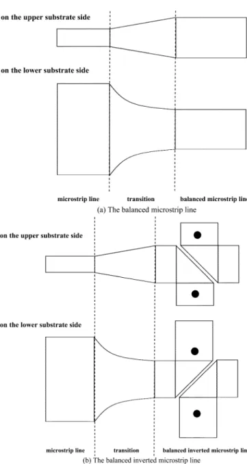
As shown in Fig. 5(a), the ground plane width of a conventional microstrip line is slowly tapered to that of a balanced microstrip line. The characteristic impedance of this balanced microstrip
Fig. 4. Diagram of the broadband feeding structure used to excite the first higher order mode of microstrip antenna. This feeding structure consists of: (i) a conventional microstrip line; (ii) a microstrip-to-balanced-microstrip-line transition; (iii) a balanced-microstrip-line T-junction; (iv) one port of the balanced-microstrip-line T-junction is changed to form an inverted balanced microsrtrip line.
line is just double that of a conventional microstrip line with a substrate half as thick as the balanced microstrip line. This microstrip-to-balanced-microstrip-line transition must be suffi-ciently long to yield a decent impedance-matching performance, especially in the lower frequency range. After this transition, a T-junction balanced-microstrip-line power divider is added, and then one of these two output ports is changed to form the inverted balanced microstrip lines. In the inverted balanced mi-crostrip lines, the positive (negative) strip on the upper (lower) substrate side is connected vertically through a via with the strip on the lower (upper) substrate side by the method illustrated in Fig. 5(b). According to this figure, each one of the positive and negative strips is terminated by a chamfered right-angled bend in the opposite directions respectively. In such a way, the posi-tions of the positive and negative strips are exchanged upside down. The lengths of the bend stubs on different substrate sides differ to compensate the reactive impedance effects induced by via holes and slanted gaps.
Notably, that the balanced and inverted balanced microstrip lines are not exactly 180 out of phase, although they have the same physical length. The electrical length of the inverted balanced microstrip line exceeds that of the balanced microstrip lines because the inverted balanced microstrip line includes an additional path that passes through the substrate. Some phase compensation techniques should be considered before these balanced and inverted balanced microstrip lines are used to feed the antenna. A simple method is to insert a delay line into the balanced microstrip line after the T-junction power divider. A vector network analyzer can measure the phase differences needed to be compensated for. In the example, the gap width is 0.15 mm; the diameter of the via is 0.6 mm; the chamfered angle is 45 and the stub dimensions are 2 mm 2.75 mm on the bottom side and 2 mm 1.6 mm on the top side. The amount of phase compensation is around 44.5 . The measured return loss of the inverted balanced microstrip lines,
HONG et al.: BROADBAND TAPERED MICROSTRIP LEAKY-WAVE ANTENNA 1925
Fig. 5. (a) Balanced microstrip line. (b) The inverted balanced microstrip line. The ground plane is shown with dotted lines. Note that two via holes are used to connect strips both in the upper and ground planes in the inverted balanced microstrip line.
as shown in Fig. 6, is observed to be better than 10 dB over a frequency range extending from dc up to 18.6 GHz. The figure also shows that the measured back-to-back feeding structure demonstrated a return loss better than 10 dB from 2.2 to 18.6 GHz. Lengthening the microstrip-to-balanced-microstrip-line transition improves this bandwidth. Parameters such as the gap width, the radius of the via-hole, the chamfered angle, and the stub length can significantly influence the bandwidth of the transmission. The gaps should be as narrow as possible, and the radius of the vias should be large to give better bandwidth performance.
IV. DESIGNEXAMPLE ANDMEASUREMENT
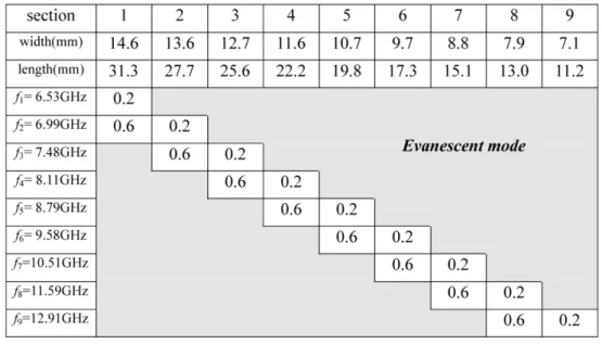
Fig. 7 shows a design example. The antenna substrate has a dielectric constant of 2.2 and a thickness of 0.508 mm. The
es-Fig. 6. Measured return loss. Solid line: the back-to back feeding structure; dashed line: the inverted balanced microstrip line.
timated survival power ratios used are and .
Therefore, the section approximately radiates around 40% of the power and the subsequent section radiates around 48% of the power at frequency for . At fre-quency , all the sections from the first to the are in the bound mode state so the power passes into the next
section. The sections beyond the are in the evanes-cent region. Under this arrangement, approximately 88 per evanes-cent
of the power is radiated in the and sections
at frequency .
In the antenna prototype, the effects of the step discontinuity and impedance mismatch, as shown in Fig. 8(a), result in serious spurious sidelobes and reduce bandwidth. Several approaches can reduce these effects [23]. For example, the antenna contour can be smoothed by directly tapering the steps [as the type I antenna in Fig. 8(b)]; or additional tapered transition sections can be inserted between adjacent original sections [as the type II antenna in Fig. 8(c)]. The latter method will greatly lengthen the antenna but the measured return loss is better. For comparison, a linearly tapered leaky-wave microstrip antenna [as the type III antenna in Fig. 8(d)] [22] also starts with a width of 14.6 mm and ends with a width of 7.1 mm; the total length of the antenna is equal to that of the type II antenna.
Fig. 9 shows the measured return loss data for antennas of types II and III. The type II antenna has a from 7 to 16.4 GHz, yielding a relative bandwidth of 2.34:1, more than an octave. This result justifies the classification of this antenna as a broadband antenna [24]. The return loss of the type III antenna is not as good as that of the type II antenna in the higher fre-quency region. The bandwidth of the type III antenna is a little less than that of the type II antenna. Figs. 9 and 10 show the measured H plane (x-z plane) radiation patterns. The radia-tion pattern at the lower frequency is very similar to that of the corresponding single section antenna. The mainlobe movement
can be checked using the relation , where is
the angle of the beam maximum measured from the endfire di-rection for an ordinary microstrip leaky wave antenna [1], [3]. From 8.2 to 10 GHz, for example, the of the mainlobe di-rection rotates toward the endfire didi-rection from 52.3 to 15.2
Fig. 7. Design example. The two parameters used to estimate power ratios at different frequency arer = 0:2 and r = 0:6.
Fig. 8. Three methods used to modify the original step discontinuities. (a) The original multisection microstrip leaky-wave antenna. (b) Type I antenna tapers the steps directly and the dotted lines show the lengths of the original sections. (c) Type II antenna inserts additional tapered sections between each two adjacent original sections. (d) Type III antenna is tapered linearly and the original sections are shown in solid lines.
for a uniform microstrip leaky-wave antenna of the same sub-strate with width of 12.7 mm. For the one with width of 11.6 mm, the of the mainlobe direction rotates toward the endfire direction from 74.1 to 31.9 . The widths of these two uniform microstrip leaky-wave antennas correspond to Sections III and IV respectively, of the proposed tapered microstrip leaky-wave
Fig. 9. Measured return loss of type II and type III tapered microstrip leaky-wave antennas.
antennas (Fig. 7). The mainlobe direction of these two uniform microstrip leaky-wave antennas is seen to shift respectively by 37.1 and 42.2 (swings down to endfire) from 8.2 to 10.0 GHz. However, in the proposed tapered microstrip leaky-wave an-tenna, the mainlobe shifts from 44 at 8.2 GHz to 22 at 10.0 GHz. The shift of the mainlobe direction is only 22.0 , which is obviously much less than that of a uniform microstrip leaky wave antenna. The mainlobe direction swings down toward the endfire direction by only 5.0 from 10.0 to 15.0 GHz. Notably when the operating frequency is increased, the gain decreases from 12.1 dBi at 8.2 GHz to 6.9 dBi at 15.0 GHz because less power flows into the tail sections. Moreover, the sidelobes grow larger at higher frequency because of the backward radiation in previous sections. Similarly, the sidelobes of the type I antenna are much larger than those of the type II antenna. This kind of backward radiation from the previous sections influences the ra-diation pattern more significantly when it occurs in sections far from the feeding end, that is, when the antenna is operated at the
HONG et al.: BROADBAND TAPERED MICROSTRIP LEAKY-WAVE ANTENNA 1927
(b)
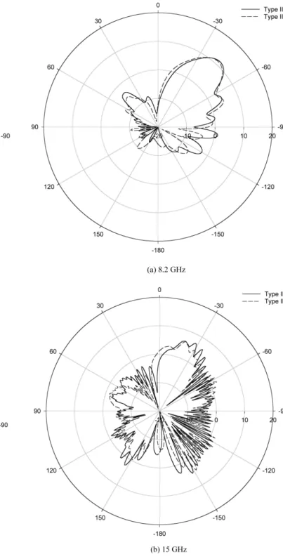
Fig. 10. H plane (x-z plane)E radiation patterns (a) of two different types of antennas (I & II) at 8.2 GHz. (b) of type II antenna at two different frequencies (at 10 and 15 GHz).
higher frequency. Additionally, the mainlobe level is reduced at the higher frequency and the numbers of sidelobes is increased. Fig. 11 reveals that the radiation patterns of the type II an-tenna are very similar to those of the type III anan-tenna. There-fore, this algorithm and design method can be used to approxi-mate effectively the linearly tapered microstrip leaky wave an-tenna which is hard to be solved analytically. The difficulties are caused by the nonuniformity of the wave in the tapered mi-crostrip profile.
Fig. 11. H plane (x-z plane)E radiation patterns of two different types of antennas (II & III) (a) at 8.2 GHz. (b) at 15 GHz.
V. CONCLUSION
The study presents a design method for broadband tapered microstrip leaky-wave antennas from 7 to 16.4 GHz with high power gain. The measured data of the inverted balanced mi-crostrip line, and the back-to-back measurement of this feeding structure, have respectively demonstrated a broadband band-width from dc, and 5 GHz, up to 18.5 GHz. The measured re-sults also demonstrate this new algorithm approximates well the linear tapered microstrip antenna.
REFERENCES
[1] A. A. Oliner and K. S. Lee, “The nature of the leakage from higher-order modes on microstrip line,” in Proc. 1986 IEEE MTT-S Int. Microwave
Symp. Dig., Baltimore, MD, 1986, pp. 57–60.
[2] W. Menzel, “A new travelling-wave antenna in microstrip,” Arch.
Elec-tron. Ubertrag. Tech., vol. 33, pp. 137–140, 1979.
[3] A. A. Oliner, “Leakage from higher modes on microstrip line with ap-plication to antenna,” Radio Sci., vol. 22, no. 6, pp. 907–912, Nov. 1987. [4] Y. D. Lin and J. W. Sheen, “Mode distinction and radiation-efficiency analysis of planar leaky-wave line source,” IEEE Trans. Microwave
Theory Tech., vol. 45, pp. 1672–1680, Oct. 1997.
[5] R. C. Johnson, Antenna Engineering Handbook. New York: McGraw-Hill, 1993.
[6] G. J. Chou and C.-K. C. Tzuang, “An integrated quasiplanar leaky-wave antenna,” IEEE Trans. Antennas Propagat., vol. 44, pp. 1078–1085, Aug. 1996.
[7] C.-K. C. Tzuang, S.-P. Liu, and G. J. Chou, “Integrated active leaky-wave antenna employing arched microstrip line,” in Proc. 8th
Asia-Pacific Microwave Conf., 1995, pp. 335–338.
[8] T. L. Chen, Y. D. Lin, and J. W. Sheen, “Mode-coupling phenomena of the even modes on a microstrip line,” IEEE Trans. Microwave Theory Tech., submitted for publication.
[9] G. J. Chou and C.-K. C. Tzuang, “Oscillator type active integrated an-tenna: the leaky mode approach,” IEEE Trans. Microwave Theory Tech., vol. 44, p. 2265, Dec. 1996.
[10] H. Shirasaki, “Optimum design by waveguide model and mode-matching technique of microstrip line taper shapes for satellite broadcast planar antenna,” in Proc. IEEE AP-S Int. Symp. Dig., 1999, pp. 238–241.
[11] V. Nalbandian and C. S. Lee, “Tapered leaky-wave ultra wide-band microstrip antenna,” in Proc. IEEE AP-S Int. Symp. Dig., 1999, pp. 1236–1239.
[12] R. Janaswamy and D. H. Schaubert, “Analysis of the tapered slot an-tenna,” IEEE Trans. Antennas Propagat., vol. AP-35, pp. 1058–1065, Sept. 1987.
[13] S. S. Zhong and N. Zhang, “Analysis of the tapered slotline antenna on a dielectric substrate,” in Proc. IEEE AP-S Int. Symp. Dig., 1998, pp. 1174–1177.
[14] P. R. Acharya, H. Ekstrom, S. S. Gearhart, S. Jacobsson, J. F. Johansson, E. L. Kollberg, and G. M. Rebeiz, “Tapered slotline antennas at 802 GHz,” IEEE Trans. Microwave Theory Tech., vol. 41, pp. 1715–1719, Oct. 1993.
[15] Y. D. Lin, J. W. Sheen, and C.-K. C. Tzuang, “Analysis and design of feeding structures for microstrip leaky wave antenna,” IEEE Trans.
Mi-crowave Theory Tech., vol. 44, pp. 1540–1547, Sept. 1996.
[16] J. M. Lin, G. J. Chou, C.-K. C. Tzuang, and S. Su, “Short leaky-wave antennas of sum and difference patterns,” Electron. Lett., vol. 32, no. 14, pp. 1247–1249, July 1996.
[17] T. L. Chen and Y. D. Lin, “Aperture-coupled microstrip line leaky wave antenna with broadside mainbeam,” Electron. Lett., vol. 34, no. 14, pp. 1366–1367, July 1998.
[18] Y. Qian, B. C. C. Chang, T. Itoh, K. C. Chen, and C.-K. C. Tzuang, “High-efficiency and broadband excitation of leaky mode in microstrip structures,” in Proc. IEEE MTT-S Int. Microwave Symp. Dig., 1999, pp. 1419–1422.
[19] R. N. Simons, R. Q. Lee, and T. D. Perl, “Non-planar linearly tapered slot antenna with balanced microstrip feed,” in Proc. IEEE AP-S Int.
Symp. Dig., 1992, pp. 2109–2112.
[20] C. S. Lee and V. Nalbandian, “Planar leaky-wave microstrip antenna,” in Proc. IEEE AP-S Int. Symp. Dig., 1997, pp. 1126–1129.
[21] J. W. Sheen and Y. D. Lin, “A leaky-mode S-parameter extraction tech-nique for efficient design of the microstrip line leaky-wave antenna,” in
Proc. IEEE MTT-S Int. Microwave Symp. Dig., 1999, pp. 175–178.
[22] J. W. Sheen, W. Hong, and Y. D. Lin, “Wide band tapered microstrip leaky-wave antenna,” in Proc. 30th Eur. Microwave Conf., vol. 2, 2000, pp. 234–237.
[23] K. C. Gupta, R. Garg, I. J. Bahl, and P. Bhartia, Micorstrip Lines and
Slotlines, 2nd ed. Norwood, MA: Artech House, 1996.
[24] W. L. Stutzman and G. A Thiele, Antenna Theory and Design, 2nd ed. New York: Wiley, 1996, ch. 6.
Wanchu Hong was born in Taiwan, R.O.C., in 1966. He received the B.S. de-gree in electrical engineering from the Feng Chia University, Taichung, Taiwan, R.O.C., in 1992 and the M.S. degree in electronic engineering in 1994 from the National Chiao Tung University, Hsinchu, Taiwan, where he is working toward the Ph.D. degree in communication engineering.
From 1994 to 1996, he was a Second Lieutenant in the Army. In 1996, he joined the TECOM Company where he was involved in RF circuit design. His research interests include computational electromagnetics, and antenna theory and communication IC design.
Tai-Lee Chen was born in Taiwan, R.O.C., in 1965. He received the B.S. degree in mathematics from the National Taiwan University, in 1989, the M.S. degree in communication engineering and the Ph.D. degree in electronics engineering from the National Chiao Tung University, Hsinchu, Taiwan, R.O.C., in 1991 and 1999, respectively.
In 1999, he was a Principal Engineer in Gemtek Technology Company, in Hsinchu, Taiwan, R.O.C., where he was involved in wireless LAN development. Currently, he is a Lecturer in the Department of Physics at National Central Uni-versity, Taiwan, R.O.C. His research interests include analytical and computa-tional electromagnetics, and antenna design.
Chi-Yang Chang was born in Taipei, Taiwan, R.O.C., on December 20, 1954. He received the B.S. degree in physics and the M.S. degree in electrical engi-neering from National Taiwan University, Taiwan, R.O.C., in 1977 and 1982, respectively, and the Ph.D. degree in electrical engineering from the University of Texas at Austin, in 1990.
From 1979 to 1980, he was with the Department of Physics, National Taiwan University, Taiwan, R.O.C., as a Teaching Assistant. From 1982 to 1988, he was with the Chung-Shan Institute of Science and Technology (CSIST) as an Assis-tant Researcher, where he was in charge of development of MICs, microwave subsystems, and mm-wave waveguide E plane circuits. From 1990 to 1995, he was back to CSIST as an Associate Researcher, and was in charge of develop-ment of uniplanar circuits, ultra broadband circuits, and mm-wave planar cir-cuits. In 1995, he joined the faculty of Department of Communication, National Chiao-Tung University as an Associate Professor. His research interests include microwave and mm-wave passive and active circuit design, planar miniaturized filter design, and MMIC design.
Jyh-Wen Sheen received the B.S. degree in control engineering and the M.S. and Ph.D. degrees in communication engineering from the National Chiao Tung University, Hsinchu, Taiwan, R.O.C., in 1991, 1993, and 1996, respectively.
In 1996, he joined the RF Communication Systems Technology Department, Computer and Communication Laboratories, Industrial Technology Research Institute (ITRI), Hsinchu, Taiwan, R.O.C., and is an RF Engineer and is cur-rently developing a miniaturized RF filter and high-gain antenna. His research interests include the analysis and design of various planar-type leaky-wave an-tennas and the investigation of surface-wave leakage phenomena of uniplanar transmission lines.
Yu-De Lin received the B.S. degree in electrical engineering from National Taiwan University, Taiwan, R.O.C., in 1985, and the M.S. and Ph.D. degrees from the University of Texas at Austin, in 1987 and 1990, respectively.
In 1990, he joined the faculty of the Department of Communication Engi-neering, National Chiao Tung University, Hsinchu, Taiwan, R.O.C., where he is currently a Professor. His current research interests include characterization and design of microwave and millimeter-wave circuits and analysis and design of microwave and millimeter-wave antennas.