The characteristics of hole trapping in Hf O 2 Si O 2 gate dielectrics with TiN gate
electrode
Wen-Tai Lu, Po-Ching Lin, Tiao-Yuan Huang, Chao-Hsin Chien, Ming-Jui Yang, Ing-Jyi Huang, and Peer Lehnen
Citation: Applied Physics Letters 85, 3525 (2004); doi: 10.1063/1.1808228 View online: http://dx.doi.org/10.1063/1.1808228
View Table of Contents: http://scitation.aip.org/content/aip/journal/apl/85/16?ver=pdfcov
Published by the AIP Publishing
Articles you may be interested in
On the electrical stress-induced oxide-trapped charges in thin Hf O 2 Si O 2 gate dielectric stack
Appl. Phys. Lett. 91, 113516 (2007); 10.1063/1.2783967
Direct tunneling stress-induced leakage current in ultrathin Hf O 2 Si O 2 gate dielectric stacks
J. Appl. Phys. 100, 094507 (2006); 10.1063/1.2372313
Characterization of C F 4 -plasma fluorinated Hf O 2 gate dielectrics with TaN metal gate
Appl. Phys. Lett. 86, 222905 (2005); 10.1063/1.1944230
Degradation mechanism of HfAlO X SiO 2 stacked gate dielectrics studied by transient and steady-state leakage current analysis
J. Appl. Phys. 97, 074505 (2005); 10.1063/1.1884253
Effects of denuded zone of Si ( 111 ) surface on current conduction and charge trapping of HfO x N y gate dielectric in metal-oxide-semiconductor devices
Appl. Phys. Lett. 85, 4723 (2004); 10.1063/1.1819994
This article is copyrighted as indicated in the article. Reuse of AIP content is subject to the terms at: http://scitation.aip.org/termsconditions. Downloaded to IP: 140.113.38.11 On: Thu, 01 May 2014 04:09:23
The characteristics of hole trapping in HfO
2/ SiO
2gate dielectrics with TiN
gate electrode
Wen-Tai Lu, Po-Ching Lin, and Tiao-Yuan Huang
Institute of Electronics, National Chiao Tung University, 1001 Ta-Hsueh Road, Hsin-Chu 300, Taiwan, Republic of China
Chao-Hsin Chien,a) Ming-Jui Yang, and Ing-Jyi Huang
National Nano Device Laboratories, 1001-1 Ta-Hsueh Road, Hsin-Chu 300, Taiwan, Republic of China Peer Lehnen
Aixtron AG, Germany
(Received 19 April 2004; accepted 20 August 2004)
The characteristics of charge trapping during constant voltage stress in an n-type metal–oxide– semiconductor capacitor with HfO2/ SiO2gate stack and TiN gate electrode were studied. We found
that the dominant charge trapping mechanism in the high-k gate stack is hole trapping rather than electron trapping. This behavior can be well described by the distributed capture cross-section model. In particular, the flatband voltage shift共⌬Vfb兲 is mainly caused by the trap filling instead of
the trap creation[Zafar et al., J. Appl. Phys. 93, 9298 (2003)]. The dominant hole trapping can be ascribed to a higher probability for hole tunneling from the substrate, compared to electron tunneling from the gate, due to a shorter tunneling path over the barrier for holes due to the work function of the TiN gate electrode. © 2004 American Institute of Physics.
[DOI: 10.1063/1.1808228]
As devices are scaled aggressively into nanometer re-gime, SiO2 gate dielectric is approaching its physical and
electrical limits. The primary issue is the intolerably huge leakage current caused by the direct tunneling of carriers through the ultrathin oxide. To substantially suppress the leakage current, high-k materials are recently employed by exploiting the increased physical thickness at the same equivalent oxide thickness (EOT). Among them, HfO2 has
been demonstrated to be highly attractive because of its rela-tively high dielectric constant共⬃25兲, sufficiently large band gap 共⬃5.9 eV兲, suitable tunneling barrier height for both electrons and holes共⬎1 eV兲, and thermal compatibility with contemporary device processes.
Even though HfO2films have been shown to be scalable
to below 1 nm,1there still exist several issues that need to be tackled before they can eventually replace SiO2 dielectric in
production. One of the most important issues for HfO2is the
charge trapping, which leads to threshold voltage instability.2–6In this work, we investigate the characteristics of charge trapping in the HfO2/ SiO2 gate stack with TiN
gate electrode. Contrary to most previous reports,2–6 it is found that hole trapping, rather than electron trapping, pre-vails in the HfO2/ SiO2 gate stack during constant voltage stressing(CVS). By employing the distributed capture cross-section model,2,3 the behavior of hole trapping can be well predicted over several decades of stress time; that is, charge trapping is caused by the hole filling of as-fabricated traps with distributed capture cross section.
The capacitors were fabricated on p-type (100) silicon wafers with local oxidation of silicon isolation. After HF-last dipping, a 1.1-nm-thick ultrathin oxide layer was grown at 800 ° C by rapid thermal annealing (RTA) in O2.
Subse-quently, an approximately 5 nm HfO2film was deposited by
atomic vapor deposition(AVD™) in an AIXTRON Tricent® system at a substrate temperature of 500 ° C, followed by N2
RTA at 500 ° C for 30 s. A 5000 Å TiN electrode was sput-tered and patterned to form gate electrodes. Then, wafers were sputtered with aluminum on the back side, and received a forming gas anneal at 400 ° C for 30 min. The EOT and initial flatband voltage of the stack before stressing are esti-mated to be 24 Å and 0.005 V from the high-frequency
共100 kHz兲 capacitance–voltage 共C–V兲 curves using UCLA
CVC method without considering quantum effect.7
Figure 1(a) shows the C–V curves of a metal–oxide– semiconductor (MOS) capacitor measured after different
a)Electronic mail: [email protected]
FIG. 1.(a) Capacitance–voltage curves and (b) conductance–voltage curves measured at 100 kHz with stress time as a parameter. The stress voltage共Vg兲 was −3.5 V. The curve labeled t = 0 s corresponds to the data before stressing.
APPLIED PHYSICS LETTERS VOLUME 85, NUMBER 16 18 OCTOBER 2004
0003-6951/2004/85(16)/3525/3/$22.00 3525 © 2004 American Institute of Physics
This article is copyrighted as indicated in the article. Reuse of AIP content is subject to the terms at: http://scitation.aip.org/termsconditions. Downloaded to IP: 140.113.38.11 On: Thu, 01 May 2014 04:09:23
CVS times. The stress voltage was −3.5 V. One observes that the C – V curve gradually shifts toward negative voltage with stress time. This tendency indicates that hole trapping is the predominant process in the gate stack during stressing. However, the negative flatband voltage shift 共⌬Vfb兲 may
arise from the emergence of positive bulk trapped charges and/or interface charges. To clarify the mechanism respon-sible for the hole trapping, the conductance of the capacitor is plotted against measuring voltage over several decades of stress time, as shown in Fig. 1(b). It is found that the con-ductance peak value and shape only change slightly with stress time. This suggests that charge trapping at the interface states does not play any significant role in ⌬Vfb for the HfO2/ SiO2gate stack during CVS.
8
Thus, we conclude that the ⌬Vfb is mainly caused by hole trappings in the bulk of
HfO2 layer. This result seems to contradict with most
previ-ous works, in which electron trappings in the high-k stacks were shown to be the dominant mechanism responsible for the threshold and flatband voltage shifts.3–6
To gain further insight into the trapping mechanism, we employ the so-called distributed capture cross-section model or stretched exponential model2,3 to describe the trapping behavior. The stretched exponential equation is given by
兩⌬Vfb兩=兩⌬Vmax兩共1−exp共−Ninj0兲兲, where 兩⌬Vmax兩, 0,  are
fitting parameters which are related to the total trap density. Here,0 represents the characteristic capture cross section,
兩⌬Vmax兩 denotes the maximum shift in 兩⌬Vfb兩 that occurs after
prolonged stressing, and Ninjdenotes the injected charge den-sity. Figure 2 shows the dependence of⌬Vfbon Ninj. It can be
clearly seen that the fitting curves(i.e., solid curves) match very well with experimental data(i.e., symbols) over several decades of Ninj. In addition, 兩⌬Vfb兩 saturates at larger Ninj when the magnitude of the stress voltage is higher than
兩−3.5 V兩. These features imply filling existing hole traps in
the high-k gate stacks. The  value is around 0.184 for all
stressing conditions indicating that hole traps in the high-k gate stacks possess larger distributed capture cross section than that of electron traps(cf.,⬃0.32);1while0is nearly
independent of voltage and its value is about 1.5
⫻10−14cm2. Moreover, it is worthy to note that兩⌬V fb兩
in-creases again as the Ninjis larger than 2⫻1020cm−2s at Vg = −4.2 V. This phenomenon is thought to be due to addi-tional traps creation.
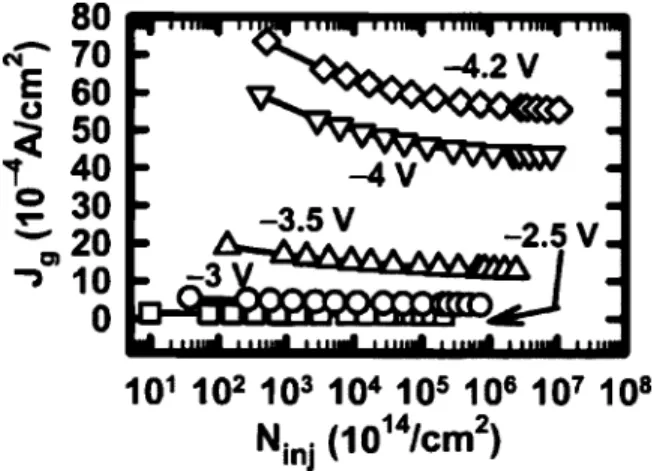
Not disregarding the success of the distributed capture cross-section model in describing the⌬Vfbduring CVS, it is still necessary to explain why the hole trapping is more likely to occur in our high-k gate stacks. We believe this can be explained by the resultant band diagram of the gate stack under Vg= −4.2 V stress, as illustrated in Fig. 3. The param-eters, including physical thicknesses, band offsets and the voltage drops across the individual insulators were deter-mined based on our TEM analyses(not shown) and the work function of TiN 共⬃4.8 eV兲 presented in previous researches.9,10It can be seen that the probability of hole tun-neling from the substrate is much higher than that of electron tunneling from the gate because of the shorter tunnel dis-tance. Therefore, the leakage current is dominated by hole injection. To reinforce this argument, the characteristics of the gate current density共Jg兲 as a function of Ninjunder
vari-ous CVS conditions (Fig. 4) show that the leakage current decreases with Ninj for all stress voltages. This is consistent
with hole dominance in the gate stack because only the trapped holes can cause leakage increase if the electron cur-rent is dominant component.
In conclusion, hole trappings are firmly observed in the HfO2/ SiO2 gate stack with TiN metal gate electrode. The ␦Vfb caused by the trapped holes can be well described by adopting distributed capture cross-section model over several decades of stress time during CVS. This phenomenon is at-tributed to the resultant asymmetric band structure, which favors hole tunneling from the substrate and, in turn, makes the gate stack more susceptible to the hole trapping.
This work was supported in part by the National Science Council of the Republic of China through Contract No. 93A0501.
1
B. H. Lee, R. Choi, L. Kang, S. Gopalan, R. Nieh, K. Onishi, Y. Jeon, W.-J. Qi, C. S. Kang, and J. C. Lee, Tech. Dig. - Int. Electron Devices Meet. 2000, 39.
2
S. Zafar, A. Callegari, E. Gusev, and M. Fischetti, J. Appl. Phys. 93, 9298 FIG. 3. Energy diagram of HfO2/ SiO2gate stack capacitor with midgap TiN
metal gate electrode under constant voltage stress共Vg= −4.2 V兲.
FIG. 4. Gate current density as a function of injection charge density for various stress voltages.
FIG. 2. Dependence of flatband voltage on injected charge density at vari-ous stress voltages; symbols are measured data; solid curves are fitting curves.
3526 Appl. Phys. Lett., Vol. 85, No. 16, 18 October 2004 Luet al.
This article is copyrighted as indicated in the article. Reuse of AIP content is subject to the terms at: http://scitation.aip.org/termsconditions. Downloaded to IP: 140.113.38.11 On: Thu, 01 May 2014 04:09:23
(2003). 3
M. Krishnan and V. Kol’dyaev, IEEE Reliability Physics Symposium Pro-ceedings, 2002.
4
W. J. Zhu, T. P. Ma, S. Zafar, and T. Tamagawa, IEEE Electron Device Lett. 23, 597(2002).
5
E. P. Gusev and C. P. D’Emic, Appl. Phys. Lett. 83, 5223(2003). 6
A. Kerber, E. Carter, L. Pantisano, M. Rosmeulen, R. Degraeve, T. Kauer-auf, G. Groeseneken, H. E. Maes, and U. Schwalke, IEEE Reliability Physics Symposium Proceddings, 2003, p. 41.
7
J. R. Hauser and K. Ahmed, AIP Conf. Proc. 449, 235(1998). 8
E. H. Nicollian and J. R. Brews, MOS Physics and Technology(Wiley, New York, 1982).
9
J. Westlinder, T. Schram, L. Pantisano, E. Cartier, A. Kerber, G. S. Lujan, J. Olsson, and G. Groeseneken, IEEE Electron Device Lett. 24, 550 (2003).
10
G. S. Lujian, T. Schram, L. Pantisano, J. C. Hooker, S. Kubicek, E. Rohr, J. Schuhmacher, O. Kilpela, H. Sprey, S. D. Gendt, and K. D. Meyer, Proceedings ESSDERC. 2002.
Appl. Phys. Lett., Vol. 85, No. 16, 18 October 2004 Luet al. 3527
This article is copyrighted as indicated in the article. Reuse of AIP content is subject to the terms at: http://scitation.aip.org/termsconditions. Downloaded to IP: 140.113.38.11 On: Thu, 01 May 2014 04:09:23