Characterization of n-GaN with Naturally Textured Surface
for Photoelectrochemical Hydrogen Generation
Shu-Yen Liu,aJ. K. Sheu,a,zJhao-Cheng Ye,a S. J. Tu,a Che-Kang Hsu,a M. L. Lee,b,zC. H. Kuo,cand W. C. Laia
a
Institute of Electro-Optical Science and Engineering, Advanced Optoelectronic Technology Center, Center for Micro/Nano Science and Technology, National Cheng Kung University, Tainan City 70101,
Taiwan b
Department of Electro-Optical Engineering, Southern Taiwan University, Tainan County 71001, Taiwan c
Institute of Lighting and Energy Photonics, National Chiao Tung University, Hsinchu 300, Taiwan
To reduce light reflection and enlarge the effective reaction surface area at the n-GaN/electrolyte interface, n-GaN epitaxial layers with naturally textured surface are utilized. The layers are combined with Cr/Au ohmic contacts on n-GaN to form working electrodes that generate hydrogen by direct photoelectrolysis of water. Although the surface reflection on the naturally textured n-GaN samples is lower than that on n-GaN epitaxial layers with flat surface, our results reveal that the photocurrent共Iph兲 and gas generation rates共Rgas兲 obtained from the naturally rough n-GaN samples are lower than those from the flat samples. The results
can be attributed to the fact that the rough n-GaN surface caused by dense surface pits leads to significant recombination of photogenerated carriers with charged defects; this occurs before carriers reach the ohmic contacts, thereby resulting in lower Iph
and Rgas. Related analyses have been performed and presented in this paper to initially explain the possible mechanism.
© 2010 The Electrochemical Society. 关DOI: 10.1149/1.3499327兴 All rights reserved.
Manuscript submitted June 11, 2010; revised manuscript received August 25, 2010. Published October 19, 2010.
The use of solar power to direct photoelectrolysis is a promising method for generating hydrogen from water.1,2Unlike oil, solar en-ergy is a renewable enen-ergy source. Water, as a product of hydrogen burning, will not cause pollution and can return to the photoelec-trolysis system via an appropriate feedback mechanism. Water pho-toelectrolysis that utilizes an illuminated semiconductor/electrolyte scheme is a potential technique for generating hydrogen. However, not all semiconductors can be developed as working electrodes to split water; certain conditions must be satisfied. For example, the conduction band-edge potential of the semiconductor material must be lower than that of the cathode-reduction half-reaction, and its valence band-edge potential must be higher than that of the anode-oxidation half-reaction.1Various types of semiconductors can satisfy these conditions. Lower bandgap semiconductors, such as InP, GaAs, and CdSe can absorb solar light more effectively. However, it has been reported that these materials easily corrode in acidic or alkaline solution.3,4 Fortunately, the band-edge potential of InxGa1−xN materials satisfies the above-mentioned condition for
splitting water.5,6 Moreover, the material is potentially resistant to aqueous solutions.7The bandgap can also vary from 3.4 to 0.7 eV once the content of In is modified, resulting in the production of a photoelectrochemical共PEC兲 cell that can fit the solar spectrum to enhance light absorption.7
GaN-based light emitting diodes共LEDs兲 have been proven that naturally formed textures on the p-GaN surface can minimize the reflection of internal light at the GaN/air interface and consequently enhance the light-extraction efficiency.8A similar concept that the GaN/sapphire-based PEC cells can be expected to lessen the reflec-tion of incident light at the GaN/air interface and consequently en-hance the photocurrent. However, these two cases have a substantial difference, which is the position of the active regions. For the GaN/ sapphire-based LEDs, the active regions are positioned at the InGaN/GaN multiple quantum well共MQW兲 interfaces, while for the PEC cells, the regions are situated in the GaN/electrolyte interfaces. Therefore, structural defects on the surface layer would produce different effects on the devices’ performance. In general, wet etching and/or dry etching techniques are employed to form a variety of textured surfaces on the GaN samples. However, the etching process can easily cause surface damage. To prevent surface damage on the etched n-GaN layers, the n-GaN epitaxial layers can be grown with a naturally roughed surface or on a selective masked area to reduce
light reflection on the sample surface compared with the flat-surfaced n-GaN layers. Waki et al. have reported that patterned n-GaN epitaxial layer formed by selective area regrowth with metal stripes can be used to achieve direct photoelectrolysis of water and increase the working area.5This study uses n-GaN epitaxial layers with abundant, naturally formed pits on the surface combined with Cr/Au bilayer metals to form the working electrodes.8,9The surface pits are on a submicron scale; therefore, the reflectance of incident light at the GaN/electrolyte interface can be reduced. Further, GaN samples with textured surface must possess a larger effective work-ing area than the samples with flat surface. Comparative analyses of spectral reflection, photoluminescence共PL兲, and electrical properties between the naturally roughed and flat n-GaN samples are per-formed to explain the origin of the results. One can thus select between the increase or decrease of light absorption or reflection on one hand and material quality on the other hand for the improve-ment of performance of GaN/sapphire-based PEC cells.
Experimental
Two types of n-GaN epitaxial layers were grown on sapphire substrate to fabricate the PEC cells. One had dense surface pits and another had a specular surface. With the exception of growth tem-perature, the growth parameters between these two n-GaN epitaxial layers were the same. In other words, the samples with surface pits were grown at a lower temperature 共approximately 900°C兲 com-pared with the samples with flat surface, which were grown at a higher temperature 共approximately 1000°C兲. The dense V-shaped surface pits of the former samples can be attributed to the small diffusion length of Ga atoms. The small diffusion length of Ga at-oms prevents the substance from migrating to proper locations at low temperature. The growth conditions in detail had been reported in earlier studies.10,11
Subsequently, a bilayer metal of Cr共50 nm兲/Au 共250 nm兲 was deposited on the n-GaN epitaxial layers to form ohmic contact of the working electrodes. Samples with textured and flat surfaces are la-beled as PEC-1 and PEC-2, respectively. A potentiostat 共Autolab-PGSTAT128N兲 was employed to supply the external bias. The cur-rent density was measured to evaluate the electrical properties of the PEC cells. A 300 W Xe lamp was utilized as the light source and 1 mol/l NaCl was used as the electrolyte at room temperature. A Ag/AgCl reference electrode and a platinum 共Pt兲 wire counter elec-trode were used to measure potential. The bias voltage was applied to the working electrode with respect to the Ag/AgCl reference electrode. Hydrogen gas was generated at the Pt wire counter
elec-z
E-mail: [email protected]; [email protected]
Journal of The Electrochemical Society, 157共12兲 H1106-H1109 共2010兲 0013-4651/2010/157共12兲/H1106/4/$28.00 © The Electrochemical Society
H1106
) unless CC License in place (see abstract).
ecsdl.org/site/terms_use
address. Redistribution subject to ECS terms of use (see
140.113.38.11
trode. Gases were collected over water and a gas chromatograph 共Agilent-6850兲 was used to determine the composition of the gener-ated gases. Reflection spectra and room-temperature photolumines-cence measurements were also performed to determine the reflectiv-ity and crystal qualreflectiv-ity of the samples, respectively.
Results and Discussion
Figure 1 illustrates the typical scanning electron microscopy 共SEM兲 images obtained from the samples. Figure1aexhibits dense V-shaped pits on the surface, while Fig.1bpresents the SEM image obtained from the flat sample. In principle, the oblique facets of the V-shaped pits should be beneficial for light trapping and increasing
effective reaction area. Figure 2presents the reflection spectra ob-tained from the surfaces of the n-GaN layers. The naturally textured sample possesses lower reflectivity when the incident light wave-lengths are shorter than 365 nm. This phenomenon can be attributed to the fact that n-GaN layers consisting of dense V-shaped pits on the surface can result in a better light trapping effect compared with the samples with flat surface. Theoretically, the PEC-1 is expected to produce higher photocurrent compared with the PEC-2. However, the experimental results are inconsistent with expectations.
Figure3demonstrates the photocurrent densities of PEC-1 and PEC-2 as a function of external bias voltage共Vext兲. The
photocur-rent density of PEC-1, being markedly lower than PEC-2, suggests the negative effect arising from material defects in PEC-1, which will counteract the contribution of enhanced light trapping effect and increased effective work area. The formation of V-shaped pits ap-pears to be a result of surface termination of dislocations,8which occurs along the growth direction, owing to a large lattice mismatch between the GaN and the sapphire. On the other hand, it has been suggested that acceptorlike states exist in the vicinity of dislocations and are responsible for the locally high reverse leakage current in GaN Schottky barrier diodes.12The charged defects will affect the carrier transport via scattering and/or recombine with the photoge-nerated carriers. This results in degradation of the photocurrent and gas generation rates.
Figure4displays the room-temperature photoluminescence spec-tra obtained from the samples. The yellow luminescence can be observed from the n-GaN with naturally textured surface. The PL result implies that the material quality of PEC-2 is better than that of PEC-1, which is consistent with the observation based on the
mi-Figure 1. 共Color online兲 The typical SEM images taken from the samples. 共a兲 shows a plurality of V-shape pits on the surface of the sample PEC-1. The inset shows an enlarged inspection of a V-shaped pit which has a submi-crometer scale.共b兲 shows the SEM image taken from the sample PEC-2.
Figure 2.共Color online兲 The reflection spectra taken from the surfaces of the n-GaN layers.
Figure 3. 共Color online兲 Typical current–potential curves of PEC-1 and PEC-2.
Figure 4. 共Color online兲 The room-temperature PL spectra taken from the samples.
H1107
Journal of The Electrochemical Society, 157共12兲 H1106-H1109 共2010兲 H1107
) unless CC License in place (see abstract).
ecsdl.org/site/terms_use
address. Redistribution subject to ECS terms of use (see
140.113.38.11
croscopy images in Fig. 1. In other words, the dislocation-related surface pits, which are formed by low-temperature epitaxial growth, may contain a number of defect states contributing to the yellow emission. It has been reported that the sources of yellow emission from GaN epitaxial layers are either the dislocations at low-angle grain boundaries in the material or the point defects which nucleate at the dislocations.13The dislocation-related defects degrade both the optical property and the electrical property of the GaN samples. Figure3, particularly the lower photocurrent density observed in the PEC-1, suggests that the photogenerated carriers significantly re-combine with the dislocation-related charged states before they reach the ohmic contacts. Although the dislocation-related defect states generally exist in the GaN layers grown on sapphire, the de-fect density is strongly dependent on growth conditions.
The initial motivation of this study is to create an n-GaN with naturally textured surface to enhance the light trapping effect and expand the effective reaction area at the GaN/electrolyte interface to increase the photocurrent in the PEC cells. However, experimental results indicate that the positive effect from samples with naturally textured surface is leveled off by the recombination of the photoge-nerated carriers and the dislocation-related states, which is different from the result from GaN-based LEDs. Moreover, light-extraction efficiency can be significantly improved by adding natural textures to the p-GaN top layer.8It has been extensively discussed and ac-cepted that the InGaN-based blue/green LEDs’ emission efficiency is weakly sensitive to structural defects density.14This is true even when the density is as high as 109–1010cm−2, which is six orders of
magnitude higher than conventional AlGaAs or AlGaInP LEDs. A popular model has been proposed to explain why the highly defec-tive InGaN materials can exhibit defect-insensidefec-tive emission charac-teristics. The presence of InN-rich or pure InN clusters in InGaN quantum well assumes the role of quantum dot-like localized states to confine the injected electron-hole pairs, which have recombined radiatively without diffusing toward the dislocations.15
In the PEC devices, the photogenerated carriers in the n-GaN layers need to diffuse away from the defects to reduce the probabil-ity of recombination before they reach the ohmic contact electrodes and external circuit. However, the screening of carriers in the local bandgap variation is absent because of the lack of indium fluctuation.15For an InGaN-based emitter with high indium content, the injected carriers can quickly and easily reach the active layer, owing to the external bias field. They can then spread into the lo-calized bandgap minimum formed by In-rich clusters to prevent the carriers from recombining with the defects.15 In contrast to the InGaN-based LEDs, the driving force of photogenerated carriers in the PEC devices diffusing to electrodes relies on the weak built-in fields resulting from the GaN/electrolyte junction or spatial distribu-tion of carriers. Therefore, a GaN-based PEC device without InN-related localized bandgap minimum in the absorption layers is con-sidered to be sensitive to structural defects. In other words, structural defects play the role of carrier killer in the PEC devices. Edge dislocations in n-GaN are suggested to be negatively charged,12,16while the low transverse mobility in GaN is proposed to have been caused by the scattering of electrons at charged dislo-cation lines. Filled traps along threading dislodislo-cation lines serve as coulomb scattering centers.17For vertical devices such as LEDs, the effect of scattering of electrons at threading dislocation lines must be more minor than that of lateral devices, such as field-effect transistors.17However, for the PEC devices in this study, the photo-generated electrons are transported laterally before being collected by the ohmic contact electrodes. Therefore, scattering by the charged dislocation lines will result in a reduction of electron mo-bility, thereby reducing the diffusion length. As a result, the photo-current density of PEC-1 is markedly lower than that of PEC-2, even if the PEC-1 has a lower light reflection, as illustrated in Fig.2and
3. Moreover, the gas generation rates at zero external bias for PEC-1 and PEC-2 are 2.1 and 4.5 cm3/hr, respectively, which are consistent
with the photocurrent density obtained from these PEC devices. In addition to the issue of carrier mobility, the flatband potential
for application of PEC devices in water splitting reaction18 is equally important. In this study, the flatband potential of PEC cells with the naturally roughed or flat n-GaN as the working electrodes was evaluated by Mott–Schottky plots. This method involves mea-suring the apparent capacitance as a function of applied potential under depletion condition. Subsequently, the flatband potential can be extracted based on the Mott–Schottky relationship18
1 Csc2 = 2 e0N
冉
E − EFB− kT e冊
关1兴where Cscis the capacitance of the space charge region, is
dielec-tric constant of the semiconductor,0is permittivity of free space, N is donor density for an n-type semiconductor, E is the applied po-tential, and EFBis the flatband potential. For a given semiconductor
and electrolyte, there exists a unique potential drop between the surface and the neutral bulk region. The unique potential refers to the flatband potential of EFB. To extract the EFB, one has to use an
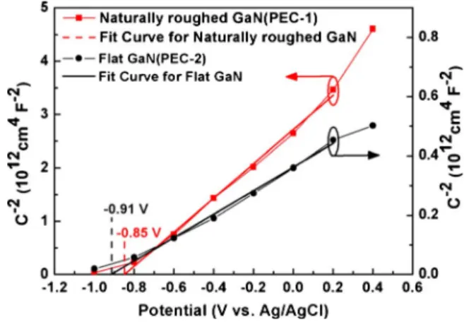
equivalent circuit to fit the experimental data and then derive the capacitance values at the different applied potential.19 Figure 5
shows the typical Mott–Schottky plots taken from the PEC-1 and PEC-2 in the dark. According to the Mott–Schottky plots, the EFB
value of PEC-1 and PEC-2 are −0.85 and −0.91 V, respectively. Considering the energy band diagram at the n-GaN/NaCl electrolyte interface, a large and negative EFB is desirable because large EFB
means that a large built-in field near the n-GaN/NaCl electrolyte interface can prompt the photogenerated electrons drifting to ohmic contacts共Cr/Au兲. In other words, the large EFBwill enable photo-generated electrons to have small transit time before they reach the Pt electrode to generate hydrogen. Carrier transport will be domi-nated by diffusion if the EFBis relatively small. Owing to this, the
photocurrent strongly depends on material quality because photoge-nerated electrons might recombine with defect states before they reach the Pt electrode.18Experimental results indicate that the EFB
extracted from the Mott–Schottky plots is consistent with the mea-sured current–potential curves of PEC-1 and PEC-2, as illustrated in Fig.3and5. In fact, a smaller EFBshould, in principle, corresponds to a lower surface carrier concentration共i.e., a smaller energy dif-ference between Fermi level and conduction band edge兲. PEC-1 with naturally roughed surface should have different surface states compared with the PEC-2 with flat surface. In other words, nega-tively charged dislocations in the naturally roughed n-GaN samples lead to a substantial compensation between free carriers and the defect-related charged states. This results in a reduction of surface carrier concentration. Therefore, the lower photocurrent and gas generation rates observed from the PEC-1 could give an edification that one should make a compromise between the light trapping and the material quality in the GaN-based PEC systems for enhancing their conversion efficiencies.
Figure 5.共Color online兲 The Mott–Schottky plots for naturally roughed and flat n-GaN samples in the dark and in 1 M NaCl electrolyte.
H1108 Journal of The Electrochemical Society, 157共12兲 H1106-H1109 共2010兲
H1108
) unless CC License in place (see abstract).
ecsdl.org/site/terms_use
address. Redistribution subject to ECS terms of use (see
140.113.38.11
Conclusions
In summary, the motivation of this study was to utilize GaN PEC cells featuring dense V-shaped pits on the surface to reduce light reflection and to increase the effective reaction area at the GaN/ electrolyte interface. However, experimental results indicate that the photocurrent共Iph兲 and gas generation rate 共Rgas兲 obtained from the naturally roughed n-GaN samples were lower than those of the flat samples. The positive effect of PEC cells on the naturally textured surface has been observed to be leveled off by the increased dislocation-related defects. In addition to the issue that carrier mo-bility will be reduced by scattering,16defect-related surface states have been shown to affect the EFB. The formation of V-shaped sur-face pits grown at a relatively low temperature will inevitably inten-sify the generation of dislocation-related defects. Since the inherent properties of high-defect density in the GaN/sapphire-based materi-als are difficult to overcome, it is possible to increase the efficiency of GaN-based PEC devices by naturally texturing the sample surface and by passivating defects either during the material growth or post-treatment.
Acknowledgments
This work has been granted by Frontier Materials and Micro/ Nano Science and Technology Center, NCKU. The authors would also like to acknowledge the National Science Council for the finan-cial support and provision of the research grant NSC 97-2221-E-006-242-MY3 and 98-2221-E-218-005-MY3.
National Cheng-Kung University assisted in meeting the publication costs of this article.
References
1. A. J. Nozik and R. Memming, J. Phys. Chem., 100, 13061共1996兲. 2. J. A. Turner, Science, 285, 687共1999兲.
3. A. J. Nozik, J. Cryst. Growth, 39, 200共1977兲.
4. R. C. Kainthla, B. Zelenay, and J. O’M. Bockris, J. Electrochem. Soc., 134, 841 共1987兲.
5. I. Waki, D. Cohen, R. Lal, U. Mishra, S. P. DenBaars, and S. Nakamura, Appl.
Phys. Lett., 91, 093519共2007兲.
6. J. Li, J. Y. Lin, and H. X. Jiang, Appl. Phys. Lett., 93, 162107共2008兲. 7. J. Wu, W. Walukiewicz, K. M. Yu, J. W. Ager III, E. E. Haller, H. Lu, and W. J.
Schaff, Appl. Phys. Lett., 80, 4741共2002兲.
8. C. M. Tsai, J. K. Sheu, P. T. Wang, W. C. Lai, S. C. Shei, S. J. Chang, C. H. Kuo, C. W. Kuo, and Y. K. Su, IEEE Photon. Technol. Lett., 18, 1213共2006兲. 9. M. L. Lee, J. K. Sheu, and C. C. Hu, Appl. Phys. Lett., 91, 182106共2007兲. 10. C. M. Tsai, J. K. Sheu, W. C. Lai, Y. P. Hsu, P. T. Wang, C. T. Kuo, C. W. Kuo, S.
J. Chang, and Y. K. Su, IEEE Electron Device Lett., 26, 464共2005兲.
11. L. W. Wu, S. J. Chang, Y. K. Su, R. W. Chuang, Y. P. Hsu, C. H. Kuo, W. C. Lai, T. C. Wen, J. M. Tsai, and J. K. Sheu, Solid-State Electron., 47, 2027共2003兲. 12. J. K. Sheu, M. L. Lee, and W. C. Lai, Appl. Phys. Lett., 86, 052103共2005兲. 13. F. A. Ponce, D. P. Bour, W. Gotz, and P. J. Wright, Appl. Phys. Lett., 68, 57共1996兲. 14. S. D. Lester, F. A. Ponce, M. G. Craford, and D. A. Steigerwald, Appl. Phys. Lett.,
66, 1249共1995兲.
15. S. Nakamura, Science, 281, 956共1998兲.
16. D. Cherns and C. G. Jiao, Phys. Rev. Lett., 87, 205504共2001兲.
17. N. G. Weimann, L. F. Eastman, D. Doppalapudi, H. M. Ng, and T. D. Moustakas,
J. Appl. Phys., 83, 3656共1998兲.
18. M. Radecka, M. Rekas, A. Trenczek-Zajac, and K. Zakrzewska, J. Power Sources, 181, 46共2008兲.
19. M. Ono, K. Fujii, T. Ito, Y. Iwaki, A. Hirako, T. Yao, and K. Ohkawa, J. Chem.
Phys., 126, 054708共2007兲.
H1109
Journal of The Electrochemical Society, 157共12兲 H1106-H1109 共2010兲 H1109
) unless CC License in place (see abstract).
ecsdl.org/site/terms_use
address. Redistribution subject to ECS terms of use (see
140.113.38.11