A Decorrelating Design-for-Digital-Testability
Scheme for
6 1 Modulators
Hao-Chiao Hong, Member, IEEE, and Sheng-Chuan Liang, Student Member, IEEE
Abstract—This paper presents a novel decorrelating
design-for-digital-testability(D3T) scheme for 6 1 modulators to enhance the test accuracy of using digital stimuli. The input switched-capac-itor network of the modulator under test is reconfigured as two or more subdigital-to-charge converters in the test mode. By properly designing the digital stimuli, the shaped noise power of the digital stimulus can be effectively attenuated. As a result, the shaped noise correlation as well as the modulator overload issues are alleviated, thus improving the test accuracy. A second-order 6 1 modu-lator design is used as an example to demonstrate the effectiveness of the proposed scheme. The behavioral simulation results showed that, when the signal level of the stimulus tone is less than 5 dBFS, the signal-to-noise ratios obtained by the digital stimuli are infe-rior to those obtained by their analog counterparts of no more than 1.8 dB. Circuit-simulation results also demonstrated that theD3T scheme has the potential to test moderate nonlinearity. The pro-posedD3T scheme has the advantages of achieving high test accu-racy, low circuit overhead, high fault observability, and the capa-bility of conducting at-speed tests.
Index Terms—Analog digital conversion, built-in self-test
(BIST), CMOS mixed-mode circuits, design-for-testability (DFT), integrated-circuit testing, sigma–delta modulation.
I. INTRODUCTION
A
MONG VARIOUS analog-to-digital converter (ADC) architectures, modulator is a popular one for implementing high-resolution ADCs because of its robustness against circuit imperfections [1]. They are widely used in low-and medium-speed applications such as instrumentation, audio, and xDSL. Traditionally, testing such high-resolution ADCs is expensive and troublesome because of the requirements of the high-end mixed-signal automatic test equipment (ATE), a long test time induced by the sequential mixed-signal test flow, and an ultralow-noise testing environment [2].Functional-test-based built-in self-test (BIST) schemes are appealing approaches to reduce the testing cost [3]–[6]. The idea is to simply implement the necessary high-performance analog-stimulus generator (ASG) on-chip in order to digitalize all the input/output (I/O) interfaces during testing. The func-tional-test-based feature of such BIST systems ensures that the test results are both detailed and flexible. In addition, unifying the testing interfaces into purely digital ones saves the testing
Manuscript received January 9, 2007; revised January 30, 2008. First pub-lished June 6, 2008; current version pubpub-lished February 4, 2009. This work was supported by the National Science Council, Taiwan, under Grant NSC93-2215-E009-050 and Grant NSC94-2215-E009-081. This paper was recommended by Associate Editor I. Bell.
The authors are with the Department of Electrical and Control Engineering, National Chiao Tung University, Hsinchu 300, Taiwan (e-mail: hchong@cn. nctu.edu.tw).
Digital Object Identifier 10.1109/TCSI.2008.926986
cost. The costly mixed-signal ATE, now, can be replaced with a cheaper digital one. The test time may also be reduced because a concurrent mixed-signal test flow is possible. Moreover, the off-chip environmental interferences are alleviated which makes the loadboard design easier.
The key requirements of a successful functional-test-based BIST implementation include the following conditions.
1) High test accuracy: The test stimuli generated by the em-bedded ASG must have a higher signal-to-noise-and-dis-tortion ratio (SNDR) than the circuit under test (CUT) can achieve. Otherwise, the ASG will dominate the test results rather than the CUT itself.
2) Low cost: The additional circuits for testing purpose should be robust enough so as not to reduce the production yield, and their hardware overhead should be small in order to save the fabrication cost.
3) High fault observability: All components active in normal operation should be excited during testing as well as for propagating the possible faulty effects to certain observ-able outputs.
4) At-speed test capability: The test scheme should not im-pose any extra load on the timing-critical components, e.g., operational amplifiers (OPAMPs), in order to test the CUT at the rated speed.
Many researches focused on implementing the embedded ASG cost effectively [4], [7]–[15]. They can be classified into the following categories: employing the available on-chip multibit digital-to-analog converter (DAC) [4], [7], [8], using a ramp waveform generator [9], [10], and exerting an exponential waveform generator [11]. Applying a single-bit DAC followed by an analog antialiasing filter is another attractive approach [3], [12]–[14], [16].
In [17], a -modulation-based design-for-digital-testa-bility (DfDT) scheme for modulators that meets most of the key requirements aforementioned has been proposed. At an oversampling ratio (OSR) of 128, the digital stimulus is able to measure a signal-to-noise ratio (SNR) of the second-order modulator under test (MUT) higher than 76 dB. Yet, the mea-sured SNRs by the digital stimuli are still inferior to those using their analog counterparts by 0.7–7.6 dB, depending on the signal level of the stimulus tone. The peak SNDR of the digital tests was obtained by the 6-dBFS stimulus. Rolindez et al.[15] pro-posed an alternative implementation that can accept pure digital stimuli. Their measurement results also showed that the signal levels of the digital stimuli had better not to exceed 12 dBFS; otherwise, the tested SNDRs of the digital tests will significantly degrade [18].
In this paper, we propose a decorrelating DfDT scheme for general switched-capacitor (SC) modulators
Fig. 1. Schematic of the original DfDT second-order601 modulator proposed in [17].
that improves the test accuracy of using digital stimuli, while it preserves the advantages of the original DfDT scheme such as having a small hardware overhead, high fault observability, and the capability to perform at-speed tests. Section II reviews the original DfDT scheme and explains the root causes of the test accuracy degradation when applying the digital stimuli. Based on the results, Section III introduces the proposed scheme and its operation principles. Section IV discusses how to design the circuits as well as the tests of the modulators. A second-order modulator design modified from [17] was used as an example. Behavioral and circuit simula-tions were conducted to demonstrate the ’s superiority in Section V. Finally, Section VI draws our conclusions.
II. REVIEWS OF THEDFDT MODULATOR
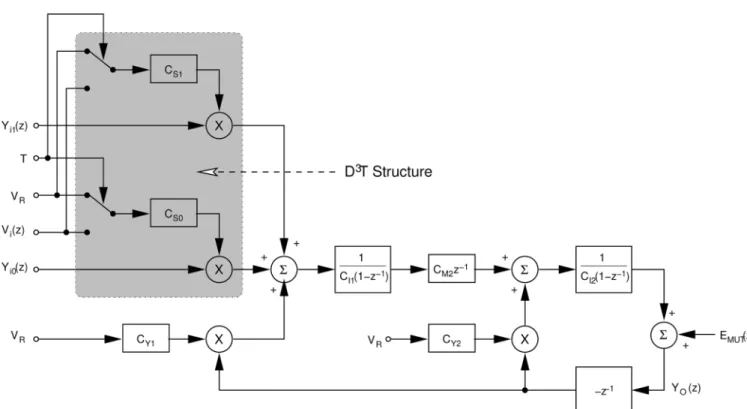
Fig. 1 shows the schematic of the DfDT second-order modulator proposed in [17]. This schematic is identical to that of a normal modulator except for the DfDT structure indi-cated by the shaded region. The DfDT circuit is modified from the original one in the normal modulator by adding the four additional switches, including to . The control sig-nals of the switches in the DfDT structure are also modified.
The DfDT scheme operates as follows. The test-mode control signal sets the operation mode. When is set to zero and the digital stimulus is fixed on one, the switches to are off, and the modulator operates in the normal mode. Fig. 2(a) and (b) shows the DfDT circuit states in the two nonoverlapped phases. During , the sampling capacitors and sample the analog inputs and , respectively. During , the sam-pled charge will be integrated by the first integrator. In other words, the analog stimulus source sends a total charge of
(1) to the first integrator in the th cycle, where
and .
Setting will turn off the switches and and
makes the modulator operate in the test mode. Now, the sam-pling capacitors and samples the reference voltages
and , respectively. The sampled charge will be inte-grated by the first integrator during according to the value of
, where .
Fig. 2(c) and (d) shows the DfDT circuit states in both phases.
Let , the first integrator in the test mode
accepts total charge of
(2) in the th cycle.
Comparing (1) with (2), it is clear that the required high-per-formance embedded ASG for testing purpose can be realized by reconfiguring the DfDT structure as a one-bit digital-to-charge converter (DCC) in the test mode. The reconfigured SC DCC is then controlled by a repetitively applied digital stimulus and generates the required high-quality analog test stimuli. The digital stimulus is synthesized by a digital bit-stream generator (BSG) which is a single-bit modulator made of either soft-ware or hardsoft-ware [16]. The single-bit characteristic of the DCC ensures that the generated stimuli have no nonlinearity issue. Since both normal and test modes have the same signal paths, the inherent nonlinearity of the circuits has similar impacts on the modulator’s outputs. The digital stimuli, thereby, are poten-tially able to provide compatible measurement results with those of conventional analog tests.
A. Analysis of the DfDT MUT
To analyze the DfDT MUT, the signal-flow-graph-analysis method [19] was adopted. Each of the switched capacitor shown in Fig. 1 can be modeled as if it has a transfer function of , where represents the capacitance value it consists of. If the input of the switched capacitor is a dc voltage, the transfer func-tion reduces to . To simplify the expressions, let us define
, ,
, , and .
We also define the normalized binary digital signals and as
Fig. 2. Circuit operation of the DfDT circuits and the first summing integrator in both modes. The DfDT circuits are highlighted in the shaded area. (a) During active8 in the normal mode. (b) During active 8 in the normal mode. (c) During active 8 in the test mode. (d) During active 8 in the test mode.
Fig. 3. Signal flow graph of the DfDT second-order601 modulator.
whose values are either 1 or 1 instead of 1 or 0. By assuming that the quantization noise is white and additive, the comparator can be modeled as a quantization noise source . The complete signal flow graph of the DfDT second-order modulator is shown in Fig. 3.
The I/O relationship of the test-mode-enabled MUT can be easily derived according to Fig. 3. The result is
(4) where
(5)
For convenience, (4) is usually normalized with respect to and can be rewritten as
(6) Since is the output of a digital modulator, it has a similar I/O relationship to (6) which is expressed as
(7)
In (6) and (7), and stand for the
signal transfer functions (STFs), and
are the noise transfer functions (NTFs), and and symbolize the quantization noises of the BSG and
Fig. 4. Measured SNR of the DfDT601 modulator shown in Fig. 1, [17].
MUT, respectively. Substituting the in (6) with (7), the I/O relationship of the test-mode-enabled MUT is derived to be
(8) Note that both quantization noise sources are respectively shaped by their NTFs. These noise-shaping terms attenuate most of the quantization noise power out of the passband. Intuitively, if the two shaped noise were uncorrelated and we make
(9) in the passband, then the passband response of the test-mode-enabled MUT could be approximated by
(10) Equation (10) is similar to that of the MUT operating in the normal mode. It implies that the digital stimuli may have sim-ilar responses to their analog counterparts in the passband. As a result, the DfDT MUT may be accurately tested by the digital stimuli. The requirement of (9) can be met by selecting a suit-able BSG structure such as a higher order modulator. B. Root Causes of the SNR Degradation in Digital Tests
However, the measurement data shown in Fig. 4 indicate that the DfDT MUT reported somewhat lower SNRs with the digital stimuli than with their analog counterparts [17]. The differences are more significant when the signal level of the stimulus tone becomes higher. Since the only difference between the analog stimulus and the digital one is the shaped noise generated by the
BSG, it concludes that the additional shaped noise in the digital stimulus leads to the MUT’s SNR degradation in the test mode. In fact, two mechanisms including the shaped-noise correlation between the BSG and MUT and the modulator overload degrade the test accuracy using the digital stimuli. We will explain about them in the following.
1) Shaped-Noise Correlation: An essential assumption in deriving (10) is that the shaped noises
and were uncorrelated. If
the correlation exists, the total in-band shaped noise power will be higher than the sum of those calculated from each term [20]. Unfortunately, the shaped-noise correlation does exist. The reason is that both the quantization noise sources are high-pass filtered by their noise-shaping terms; consequently, the two shaped noises have similar spectra. Since the correla-tion between two random processes indicates how similar they are, the two shaped noises are correlated to some degree. Its significance depends upon the circuit design of the MUT and the tests.
No analytical method can well predict the shaped-noise corre-lation due to the nonlinear nature of practical modulation loops. Only behavioral simulations with a suitable behavioral model give us reliable predictions. The fully settled linear be-havioral plus noise (FSLB N) model is such a model [21]. It has been shown to be able to precisely predict the SNR per-formance of the DfDT MUT in the range of 0.05– 2.2 dB, no matter what mode the MUT operates in [21]. In the rest of this paper, all behavioral simulations are conducted with the FSLB N model.
2) Modulator Overload: Another mechanism which de-grades the tested SNRs of the MUT by the digital stimuli is that the MUT may be overloaded when the input power is high. Recall that modulators produce pulse-density-modulated bit-stream outputs; in other words, the signal level of the input sample is represented by the output’s pulse density. Since the maximum pulse density is one, there is a signal-level limit of the input that the MUT can accept without performance degradation. A more general view of this criterion is from a power perspective. Because the output power of the MUT is limited, the sum of the input power and the shaped quantization noise power has an upper bond. That is
(11) where represents the upper bond, stands for the maximum input power allowed, and symbolizes the total shaped quantization noise power of the MUT accumulated from dc to half the sampling rate. Let be the quantization step and assume that the quantization noise were uniformly distributed and uncorrelated to the input, it can be shown that
(12) The NPG above is named as the noise power gain of the MUT which is defined as
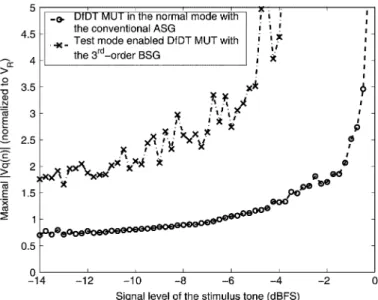
Fig. 5. MaximumjV (n)j of the DfDT MUT versus the signal level of the stimulus tone.
By (12) and normalizing and to the full-scale input power , (11) can be rewritten to be
(14) The notations and denote that these values are normalized. Similar criteria can be found in designing general – modulators. For instance,[22] uses the following normal-ized equation as a criterion to design the NPG:
(15) Here, is a constant depending on the structure of the target modulator design.
Although (15) is not an analytical result but an empirical con-clusion based on observing the results of many simulations, it is quite similar to (14). The difference between (14) and (15) comes from the discrepancy between theory and practice. When deriving (14), the quantization noise was assumed to be un-correlated to the input. In practice, they do have some corre-lation. Therefore, some modifications are necessary to compro-mise with the correlation.
For the DfDT MUT operating in the test mode, its input con-tains the test stimulus as well as the additional shaped noise gen-erated by the BSG. As a result, the digital stimulus has higher power than its analog counterpart. According to (11), the higher stimulus power is more likely to overload the MUT.
To find out when the DfDT MUT will be overloaded, Fig. 5 shows the simulation results of the maximal versus the signal level of the stimulus tone, where denotes the ab-solute value of the input voltage of the MUT’s quantizer. The pure analog sinusoidal stimuli and the third-order digital stimuli are examined.
A modulator is said to be overloaded if it produces a quantization noise out of . For the design example, the MUT is overloaded if any one of its is larger than . According to Fig. 5, the MUT operating in the normal mode is overloaded when the signal level of the analog stimulus is larger
than 1.5 dBFS. Once the MUT is overloaded, the approxima-tion that the quantizaapproxima-tion noise has a uniform distribuapproxima-tion is get-ting worse. The total harmonic distortion plus noise (THD N) power in the passband thus increases. Consequently, the peak SNR of the MUT does not appear at 0-dBFS input but some-where between 0 and 1.5 dBFS. On the other hand, the DfDT MUT operating in the test mode is overloaded at a stimulus level as low as 10 dBFS. It explains why the measured SNR curve with the digital stimuli in Fig. 4 bends down at the high stimulus levels.
III. DECORRELATINGDFDT MODULATOR
In order to alleviate the impairment effects of the shaped-noise correlation and modulator overload, an intuitive way is
to reduce the shaped noise of the
dig-ital stimulus. Since the BSG’s quantization noise is high-pass shaped, adding a low-pass filter (LPF) to the MUT by some means to filter the digital stimuli would enhance the test accu-racy using the digital stimuli.
A. Schematic of the Decorrelating DfDT Second-Order Modulator
Fig. 6 shows the schematic of the proposed second-order modulator which can provide the required LPF feature for the digital stimuli. It is modified from Fig. 1 by splitting the DfDT circuits into two identical ones. Each of them can be considered as a sub-DCC in the test mode.
There are also two operation modes. In the normal mode, the test-mode control pin is set to zero and the stimulus input pins
, are fixed on one. The switches to ,
, are turned off as a consequence. The whole MUT behaves as a normal second-order modulator.
When operating in the test mode, the test-mode control pin is set to one, thus turning off the switches and
where . The sampling capacitors ,
and now sample the reference voltages and ,
respectively. The stored charge is then transferred to the inte-gration capacitors and through either the switches and or and , depending on the digital stimuli . The rest of the MUT circuits keep the same operation as if they were in the normal mode. The proposed scheme reuses and excites all the components of the modulator in the test
mode, except for the four switches , and .
Since there is no noise margin for analog signals, every faulty effect of the parametric and catastrophic faults of the stimulated components will propagate to the primary output. As a result, it achieves high fault observability.
In addition, the test configuration does not change the loading conditions of the OPAMPs, thus providing the MUT with the capability of conducting at-speed tests.
The hardware overhead only consists of 16 switches and some digital circuits to generate the control signals, showing that the scheme is a low-cost approach. Besides, the function of a switch (turning on and off) is quite insensitive to the process variation, hence the extra circuits for testing purpose have negli-gible impact on the functional yield. Process variation may alter the turn-on resistances of the switches and result in a different
Fig. 6. Schematic of the proposedD T second-order 601 modulator.
maximum operating speed. This issue can be addressed by de-signing the switches with suitable design margins or identified by the permissible at-speed tests.
B. Analysis of the MUT
Fig. 7 shows the signal flow graph of the second-order modulator in the test mode. The shaded area points out the signal flow graph of the circuits. In fact, it is a combination of two copies of the shaded area as shown in Fig. 3. According to this figure, the normalized I/O relationship of test-mode-enabled
MUT can be derived to be
(16) where
(17)
Let and
, then (16) can be rewritten to be
(18) where is the relative input delay between the two digital
stimuli. Choosing , we have
(19) Comparing (19) with (8), an additional finite-impulse-response
(FIR) LPF term is formed to filter out some
shaped noise of the digital stimulus. In the meantime, the stimulus tone is not affected since the term has a low-pass response and a dc gain of one. The requirement
Fig. 7. Signal flow graph of the proposedD T second-order 601 modulator.
easily fitted in by choosing .
IV. DESIGN OF THEDECORRELATINGDFDT SCHEME
The proposed scheme can be extended to a more general structure. Several design parameters such as the decomposition number, the decomposition factor, the relative input delay, and the BSG structure can be designed in order to acquire the most accurate result of a test. In the following, we use the second-order modulator example to discuss the design of the MUT.
A. Decomposition Number
By applying a FIR LPF term with more taps, more shaped-noise power of the digital stimulus can be attenu-ated [23]. Hence, the digital stimulus becomes more similar to its analog counterpart. The required decorrelating LPF term can be realized by decomposing the input SC network into more sub-DCC networks. However, increasing the decom-position number of the sub-DCC networks runs the risk of inducing more in-band thermal noise power. Let and be the decomposition number and the input sampling capaci-tance in the normal mode, respectively, and let be evenly decomposed into sub-DCC networks. The total in-band thermal noise power induced by the input sampling capacitor
is in the normal mode, but each sub-DCC
network causes total in-band thermal
noise power in the test mode. If these sub-DCC networks operated independently, the total in-band thermal noise power in the test mode induced by the structure would be as high
as . The increased thermal noise power
might significantly diminish the test accuracy. For example, if , then the measured SNR of the MUT in the test mode may be 12 dB worse, even if there were neither shaped-noise correlation nor modulator-overload impairment in the test. As a result, it is suggested that the decomposition number should be kept as small as possible.
The appropriate decomposition number can be designated through extensive behavioral simulations. We take two as the de-composition number in our design example because of its sim-pler circuit implementation and satisfying accuracy.
B. Decomposition Factor
Generally speaking, it is not necessary to decompose the input sampling capacitor into two identical ones. Structurally,
the general relationship between , ,
and can be expressed as
(20) Defining the decomposition factor as
(21)
will return and
. The I/O rela-tionship of the MUT in the test mode thereby becomes
Fig. 8. Shaped-noise attenuation versus decomposition factor .
According to the equation given above, the general decorre-lating LPF term associated with the digital stimulus is
(23) Equation (23) has a flat unit-gain frequency response at low fre-quencies (close to ). Consequently, the in-band fre-quency response of the test stimulus is very similar to that in the normal mode.
To find out the suitable decomposition factor , recall that our original objective of adding the decorrelating LPF term is to filter out as much shaped-noise power of the digital stimulus as possible. It is instructive to check the relationship between and the attenuation capability of (23). Fig. 8 shows the results. The relative input delay is set to six here. Obviously,
achieves the maximum attenuation for this design. The result can be interpreted as that, to maximize the noise attenuation in certain frequency range, the most effective way is to put some real zeros in it because an FIR filter cannot provide any pole [23]. Equation (23) provides zeros on the unit circle of -do-main if and only if . Fig. 8 also shows that the scheme tolerates moderate capacitor mismatch. Capacitor mis-match between the spilt-sampling capacitors and may cause somewhat deviating from 0.5. Even though, the shaped noise of the digital stimulus can still be effectively attenuated. C. Relative Input Delay
The last design parameter needed to be determined is the rel-ative input delay between the two digital stimuli. The design scenario here is trying to put real zeros on certain frequencies to remove as much shaped-noise power of the digital stimulus as possible. A larger puts more zeros on different frequen-cies, but the effective attenuation band of each zero becomes narrower.
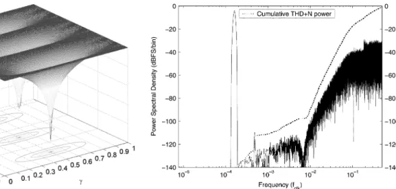
In practice, the selection of a suitable is quite complicated because of the nonlinear nature of modulation loops. Fig. 9 shows the spectrum of the 4-dBFS digital stimulus generated by the third-order BSG used in [17]. There are lots of significant spurs at the frequencies higher than one-fifth the sampling rate that are not revealed by (7). Putting a zero nearby
Fig. 9. Spectrum of the04-dBFS digital stimulus generated by the third-order BSG.
Fig. 10. Spectrum of the equivalent stimulus of theD T MUT operating in the test mode wheren = 6.
these dominant spurs would be a more effective way to cut down the shaped-noise power. However, the spectral distribu-tion of the spurs depends on the structure of the BSG as well as the signal level and frequency of the stimulus tone. Hence, we conducted extensive behavioral simulations to demonstrate that there is an appropriate with which the digital test can reveal the highest SNR of the MUT. The results will be presented in Section V.
Fig. 10 shows the spectrum of the equivalent stimulus of the MUT in the test mode. The two digital stimuli, and , are the same as that shown in Fig. 9 except for a relative input delay of six. High-frequency noise and spurs are effec-tively attenuated. Its shaped noise therefore bears less resem-blance to that of the MUT. As a consequence, the shaped-noise correlation becomes less.
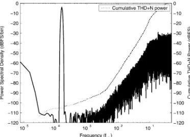
Comparing both cumulative THD N power plots as shown in Figs. 9 and 10 with each other, the total shaped-noise power of the digital stimulus is reduced by 3 dB using the scheme. Consequently, the maximal level of the stimulus tone without overloading of the MUT extends to be higher than
Fig. 11. MaximumjV (n)j of the D T MUT versus the signal level of the stimulus tone.
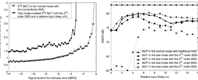
5 dBFS, as shown in Fig. 11. The test-mode-enabled MUT thus achieves high test accuracy even at high stimulus levels.
V. SIMULATIONRESULTS
To verify the scheme, behavioral simulations with the FSLB N model of the design example were conducted first. All necessary circuit parameters were according to the design of [17]. The OPAMPs were assumed having an offset voltage of 0.41 mV, an open-loop gain of 75 dB, and an output swing of 2.8 V. All transient responses were assumed to be fully settled. The thermal noise induced by the switched capacitors was also included. The frequency of the test stimulus was set to 21/128 times the sampling rate. Since the test accuracy of the digital stimulus is getting worse at a higher stimulus level, the signal level of the stimulus tone was set to 4 dBFS unless otherwise noted.
In addition to the second-order BSG candidate whose struc-ture is the same as that of the MUT, three high-order BSG can-didates were adopted from [22] to justify the importance of selecting a suitable BSG. They are the third- and fifth-order feedforward single-bit modulators and the fourth-order multiple-feedback one.
A. Selection of the Relative Input Delay, BSG, and Decomposition Number
According to (19), the maximum allowable is limited by the decorrelating LPF term, , in the STF of the test stimulus . A too large will significantly distort the stimulus tone’s response. Therefore, we only examine the less than 17. Fig. 12 shows the simulation results.
The modulator achieves better results
than the original DfDT design . Depending on the se-lected BSG structure, the optimal relative input delay is in the range of four to nine. Further increasing the relative-input-delay value does not improve the test accuracy. As has been discussed,
Fig. 12. Simulated SNR results of theD T MUT with various stimulus gen-erators and relative input delays.
a high relative-input-delay value narrows the attenuation band of each zero, thus some significant spurs may not be effectively attenuated. Behavioral simulations are thereby substantial to de-termine an adequate design using the scheme.
The combination of the fifth-order BSG with a relative input delay achieves the best test result, which is 80.2 dB. It is 6.3 dB better than that of the original DfDT scheme. The best test setup may be different when a different test stimulus or a different MUT is applied.
The second-order BSG performs worse than the third- and fifth-order BSGs, owing to its insufficient in-band attenuation capability, as we would expect according to (4). Surprisingly, the fourth-order BSG provides the worst result in this case, even worse than the second-order one. It is because the selected fourth-order BSG leaves the MUT too much shaped-noise power in the test, even with the help of the decorrelating LPF term. As a consequence, the MUT is severely overloaded. Al-though the fourth-order BSG is superior to the second-order one at low stimulus levels as shown in Table I, it is not suitable for the test which requires the 4-dBFS stimulus tone. It indicates that selecting a suitable BSG structure for a specified test is necessary.
Finally, since the test accuracy of using the digital stimulus is already within 3.1 dB for the design example, the improvement headroom by increasing the decomposition number of the scheme is limited, while it costs more hardware overhead. Hence, we only discuss the cases in which the decomposition number is two.
B. Test Accuracy
Table I lists the simulated SNR results of the MUT with various stimulus generators. The digital stimuli are applied to the MUT with the same relative input delay which is six. The results show that the digital stimuli are as linear as their analog counterparts.
The overall test errors, defined as the differences between the SNRs obtained by the digital stimuli and those of their analog
TABLE I
SIMULATEDSNR RESULTS(in decibels)OF THED T MUT WITHVARIOUS
STIMULUSSOURCES
counterparts, of the design examples with the third- and fifth-order BSGs are shown in Fig. 13.
For the low-stimulus-level tests ( 10 dBFS) where the shaped-noise correlation effect dominates, the original DfDT MUT with the third-order BSG has the worst test error of 3.4 dB. By applying the scheme, the modified MUT success-fully decorrelates the shaped noises of the BSG and the MUT. The MUT achieves test errors no worse than 1.8 dB with the same stimuli applied to the original DfDT MUT.
The scheme improves the test accuracy of the digital stimuli not only at low stimulus levels but also at high stimulus levels where the overloading effect becomes significant. Take the same third-order BSG cases as examples, Fig. 13 shows that the original DfDT scheme has the worst test error of 5.7 dB for the test stimulus whose level is not higher than 5 dBFS. On
Fig. 13. Test errors of various test schemes.
the other hand, the test errors of the MUT are not worse than 1.8 dB within the same range. About 4-dB improvement is achieved, owing to that the MUT in the test mode has a higher overload limit of its stimulus level.
Even at 4 dBFS where the overload effect is the most signif-icant, the test error of the test-mode-enabled MUT is still better than 3.1 dB. More than 5.5-dB improvement over the original DfDT scheme is achieved. Obviously, the scheme is superior to the original DfDT scheme for all kinds of tests. C. Shaped-Noise Correlation and Modulator Overload
It is interesting to examine what happened to the MUT when the 4-dBFS test stimuli were applied. Figs. 14 and 15 show the output spectra of the MUT in both modes. The corresponding cumulative THD N power plots are also shown.
Fig. 14 shows the output spectrum of the test with the con-ventional analog stimulus. In addition to the stimulus tone, the spectrum is composed of two types of noise. The thermal noise which has the property of a uniform distribution dominates at frequencies less than as shown by the flat noise floor. On the other hand, the shaped quantization noise dom-inates at higher frequencies due to the MUT’s noise-shaping characteristic.
Each output spectrum of the digital tests shown in Fig. 15 can be divided into a thermal noise floor and also a shaped-noise part. However, the shaped-noise power of the DfDT scheme is higher than the proposed scheme. In fact, all simulations of Fig. 13 show that the shaped-noise power of the DfDT scheme is higher. Recall that higher shaped-noise correlation will lead to higher shaped-noise power. We conclude that the scheme does decorrelate the shaped noise of the digital stimulus and that of the MUT.
Comparing Figs. 14 with 15, the in-band noise of the test shows a great resemblance to that of the analog test. On the other hand, their shaped noises are still somewhat different. Fig. 16 shows the cumulative THD N power plots of the three tests to gain more insights into the effects of the shaped-noise correlation. Every THD N plot can be divided into a high-slope
Fig. 14. Output spectrum of theD T second-order 601 modulator operating in the normal mode with the pure analog stimulus.
Fig. 15. Output spectra of the digital tests including the DfDT test(n = 0) and theD T test with n = 6.
Fig. 16. Cumulative THD+N power plots of different tests.
TABLE II
CIRCUIT-SIMULATIONRESULTS OF THED T MUT
segment and a low-slope segment. The shaped-noise dominates the high-slope segments while the thermal noise rules the low slope ones. The figure implies that the test errors are relative to the rated OSR of the MUT. For instance, the test error of the one in Fig. 15 is reduced from 3.1 to 1.1 dB if the OSR is increased from 128 to 256. It is because, at such an OSR, the SNR is mainly determined by the thermal noise. As a result, the shaped-noise correlation has no significant impact on the final SNR. Yet, the application determines the rated OSR and thus the test error.
D. Circuit-Simulation Results
In addition to the behavioral simulations, we also conducted circuit simulations in order to demonstrate the feasibility of the proposed scheme. The circuits shown in Fig. 6 has been simulated using HSPICE. The design adopted the same circuits used in [17] except for the structure. The OPAMPs were in-tentionally made somewhat asymmetric to induce them an offset of 4.7 mV. Due to the very long simulation time, we could only take 32 output samples for each analysis. The same 5-dBFS sinusoidal stimulus tone with a frequency of 23/32 times the clock frequency was applied to all simulations. The master clock frequency, , was set to 25 MHz. Table II summarizes the cir-cuit-simulation results.
Note that there are three major differences between the cir-cuit simulations and the behavioral simulations. First, it is hard to include the thermal noise and flicker noise into the circuit simulations. These noise sources will dither the internal signals of the MUT and may impact on the results [21]. Second, our behavioral simulations assumed that the OPAMPs have linear gains, and their outputs will be hard clamped once they exceed the defined saturation voltages. Therefore, the behavioral sim-ulation results contain less nonlinear information of the MUT. Lastly, the circuit simulations induce numerical errors while the behavioral simulations do not.
1) Testing SNR: The tested SNRs listed in Tables I and II are somewhat different. As explained earlier, the noise sources and test setups of the behavioral and circuit simulations are different. Consequently, the best relative input delay may be different. For our example, setting results in the highest SNR which is
Fig. 17. Output spectra of theD T second-order 601 modulator operating in the test mode with the third-order digital stimulus and relative input delays of zero and five.
73.2 dB. This value is only 2.2 dB lower than that of the analog test.
It is worthy to note that the circuit-simulation results of the analog test are very similar to the normal-mode results of the original DfDT design in [17]. However, the circuit simulations underestimated the performance of the DfDT MUT. The mea-surement results showed that the DfDT MUT in the normal mode achieved an SNR of 82 dB and a third harmonic below 104 dBFS [17], whereas the corresponding SPICE simula-tion gave an SNR of about 75 dB and a third harmonic around 72 dBFS. Nevertheless, the circuit-simulation results can be considered as those of a practical design whose in-band white noise is high and linearity is poor.
Fig. 17 shows the output spectra of the digital tests with and . Consistent with Fig. 16, the shaped-noise power of the proposed scheme is also lower than the original DfDT scheme. Once again, it proves that the scheme indeed helps in alleviating the shaped-noise correlation, yet their tested SNRs at an OSR of 128 are not much different.
We show the cumulative noise power plots of various tests in Fig. 18 to gain more insights into the test results. Comparing Fig. 18 with 16, the circuit simulations presented 6-dB higher in-band white noise power. The corner frequencies of the spectra at which the shaped noise becomes dominant thereby shift to the higher frequencies. At an OSR of 128, the rated passband is below the corner frequencies. Consequently, the tested SNRs are mainly determined by the in-band white noise rather than the shaped noise. That is the reason why the SNR improvement of the schemes is not so significant even though they suffer less from the shaped-noise correlation.
2) Testing Nonlinearity: Fig. 19 shows the output spectra of the MUT operating in the normal mode. The circuit simulation reported that the MUT in the normal mode has the third and the fifth harmonics of 71.7 and 83.5 dBFS, re-spectively. However, the test-mode-enabled MUT with a rela-tive input delay of zero, i.e., the original DfDT MUT, failed to reveal the harmonic distortions. The reason of the test’s impo-tence in detecting the harmonic distortion is that the digital
stim-Fig. 18. Cumulative THD+N power plots of the D T second-order 601 modulator.
Fig. 19. Output spectrum of theD T second-order 601 modulator operating in the normal mode with the conventional analog stimulus.
ulus contains significant high-frequency noise which will dither the MUT. As a consequence, the tested harmonic distortion is greatly reduced. Similar dithering techniques are commonly used for modulators to enhance their linearity [24]–[26].
Yet, testing moderate nonlinearity is also a desired goal for us. Refer to Table II, the test setup using did a good job for testing the nonlinearity although it is not the most suit-able one for testing the SNR. Fig. 20 shows the output spectrum. The tested third-harmonic distortion is 75.0 dBFS which dif-fers from the normal-mode result by only 3.3 dBFS. Setting to other nonzero values also helps. For example, the output spec-trum of the digital test with is shown in Fig. 21. The tested third and fifth harmonics are 77.8 and 86.2 dBFS, respec-tively. Both are more accurate than the results using the DfDT scheme.
Similar to the discussion of the shaped-noise correlation, it is very difficult to analyze what test setup is the most suitable for testing the nonlinearity. We conducted several simulations with different test setups and found is a good initial
Fig. 20. Output spectrum of theD T second-order 601 modulator operating in the test mode with the third-order digital stimulus and a relative input delay of one.
Fig. 21. Output spectrum of theD T second-order 601 modulator operating in the test mode with the third-order digital stimulus and a relative input delay of four.
guess. In practical applications, some tests can be conducted in advance to determine the best test setup. Then, we can find out the correlation between the test results of the scheme and those of their analog counterparts for making the final pass/fail decisions.
VI. CONCLUSION
In this paper, a novel scheme for modulators to improve their test accuracy with digital stimuli is presented. The input SC network of the MUT in the test mode is decomposed into two or more sub-DCCs that accept the -modulated bit-streams as their stimuli. With appropriate design, the digital stimuli are low-pass filtered by a decorrelating LPF term to al-leviate the shaped-noise correlation and MUT overload issues. The behavioral simulations of the second-order modu-lator example showed that the test errors of the digital stimuli are no worse than 1.8 dB when the MUT is not overloaded. Even with the 4-dBFS stimulus which severely overloads the MUT, the test error is still no worse than 3.1 dB. Circuit simu-lations also demonstrated that the scheme has the potential
to test moderate nonlinearity. In addition to the high test accu-racy, the proposed scheme also achieves the advantages of low hardware overhead, high fault observability, and the capa-bility of conducting at-speed tests in the test mode. The scheme can be easily applied to other kinds of modula-tors as well and makes them also digitally testable. Based on the proposed idea, the digitally testable designs in [18] and [27] can be modified to enhance their testing accuracy.
REFERENCES
[1] S. R. Norsworthy, R. Schreier, and G. C. Temes, Delta–Sigma Data
Converters: Theory, Design, and Simulation. Piscataway, NJ: IEEE Press, 1997.
[2] M. Burns and G. W. Roberts, An Introduction to Mixed-Signal 1C Test
and Measurement.. Oxford, NY: Oxford Univ. Press, 2001. [3] M. F. Toner and G. W. Roberts, “A BIST scheme for a SNR, Gain
tracking, and frequency response test of a sigma–delta ADC,” IEEE
Trans. Circuits Syst. II, Analog Digit. Signal Process., vol. 42, no. 1,
pp. 1–15, Jan. 1995.
[4] K. Arabi, B. Kaminska, and J. Rzeszut, “BIST for D/A and A/D con-verters,” IEEE Des. Test Comput., vol. 13, no. 4, pp. 40–49, 1996, Winter.
[5] M. Hafed and G. W. Roberts, “A stand-alone integrated excitation/ex-traction system for analog BIST applications,” in Proc. IEEE CICC, 2000, pp. 83–86.
[6] H.-C. Hong, J.-L. Huang, K.-T. Cheng, C.-W. Wu, and D.-M. Kwai, “Practical considerations in applying 60Delta modulation-based analog BIST to sampled-data systems,” IEEE Trans. Circuits Syst. II,
Analog Digit. Signal Process., vol. 50, no. 9, pp. 553–566, Sep. 2003.
[7] M. J. Ohletz, “Hybrid built-in self-test (HBIST) for mixed analog/dig-ital integrated circuits,” in Proc. IEEE Eur. Test Conf., 1991, pp. 307–316.
[8] K. Arabi and B. Kaminska, “On chip testing data converters using static parameters,” IEEE Trans. Very Large Scale Integr. (VLSI) Syst., vol. 6, no. 3, pp. 409–419, Sep. 1998.
[9] K. Arabi and B. Kaminska, “Efficient and accurate testing of analog-to-digital converters using oscillation-test method,” in Proc. Eur. Des. Test
Conf., 1997, pp. 348–352.
[10] Y.-C. Wen and K.-J. Lee, “An on chip ADC test structure,” in Proc.
DATE, 2000, pp. 221–225.
[11] H.-K. Chen, C.-H. Wang, and C.-C. Su, “A self calibrated ADC BIST methodology,” in Proc. IEEE VTS, 2002, pp. 117–122.
[12] M. F. Toner and G. W. Roberts, “A frequency response, harmonic dis-tortion, and intermodulation distortion test for BIST of a sigma–delta modulator,” IEEE Trans. Circuits Syst. II, Analog Digit. Signal
Process., vol. 43, no. 8, pp. 608–613, Aug. 1996.
[13] J.-L. Huang, C.-K. Ong, and K.-T. Cheng, “A BIST scheme for on-chip ADC and DAC testing,” in Proc. DATE, 2000, pp. 216–220. [14] M. Hafed, N. Abaskharoun, and G. W. Roberts, “A stand-alone
inte-grated test core for time and frequency domain measurements,” in Proc.
IEEE ITC, 2000, pp. 1031–1040.
[15] L. Rolindez, S. Mir, A. Bounceur, and J.-L. Carbonero, “A BIST scheme for SNDR testing of601 ADCs using sine-wave fitting,”
J. Electron. Testing: Theory Appl. (JETTA), vol. 22, no. 4–6, pp.
325–335, Dec. 2006.
[16] B. Dufor and G. W. Roberts, “On-chip analog signal generation for mixed-signal built-in self-test,” IEEE J. Solid-State Circuits, vol. 34, no. 3, pp. 318–330, Mar. 1999.
[17] H.-C. Hong, “Design-for-digital-testability 30 MHz second-order 601 modulator,” in Proc. IEEE CICC, 2004, pp. 211–214. [18] L. Rolindez, S. Mir, J.-L. Carbonero, D. Goguet, and N. Chouba, “A
stereo audio601 ADC architecture with embedded SNDR self-test,” in Proc. IEEE ITC, 2007, pp. 1–10.
[19] D. A. Johns and K. Martin, Analog CMOS Integrated Circuit Design. Hoboken, NJ: Wiley, 1996, 07030.
[20] B. Razavi, Design of Analog CMOS Integrated Circuits. New York: McGraw-Hill, 2001, 10020.
[21] H.-C. Hong, “A fully-settled linear behavior plus noise model for evaluating the digital stimuli of the design-for-digital-testability601 modulators,” J/ Electron. Test.: Theory Appl. (JETTA), vol. 23, no. 6, pp. 527–538, Dec. 2007.
[22] T.-H. Kuo, K.-D. Chen, and J.-R. Chen, “Automatic coefficients design for high-order sigma–delta modulators,” IEEE Trans. Circuits Syst. II,
[23] A. V. Oppenheim and R. W. Schafer, Discrete-Time Signal
Pro-cessing. Englewoods Cliffs, NJ: Prentice-Hall, 1989.
[24] S. Pamarti, J. Welz, and I. Gallon, “Statistics of the quantization noise in 1-bit dithered single-quantizer digital delta–sigma modulators,”
IEEE Trans. Circuits and Systems I: Regular Papers, vol. 54, no. 3,
pp. 492–503, Mar. 2007.
[25] H. Hsieh and C.-L. Lin, “Spectral shaping of dithered quantization er-rors in sigma–delta modulators,” IEEE Trans. Circuits Syst. I, Reg.
Pa-pers, vol. 54, no. 5, pp. 974–980, May 2007.
[26] J. Markus, J. Silva, and G. C. Temes, “Theory and applications of in-cremental16 converters,” IEEE Trans. Circuits Syst. I: Reg. Papers, vol. 51, no. 4, pp. 678–690, Apr. 2004.
[27] H.-C. Hong, “A design-for-digital-testability circuit structure for 601 modulators,” IEEE Trans. Very Large Scale Integr. (VLSI) Syst., vol. 15, no. 12, pp. 1341–1350, Dec. 2007.
Hao-Chiao Hong (M’04) received the B.S., M.S., and Ph.D. degrees in electrical engineering from National Tsing-Hua University, Hsinchu, Taiwan, in 1990, 1992, and 2003, respectively.
From 1997 to 2001, he was with Taiwan Semicon-ductor Manufacturing Company, where he developed mixed-signal IPs for customers and process vehicles. In August 2001, he was with Intellectual Property Li-brary Company, Hsinchu, where he was the Senior Manager of the Analog IP Department. Since Feb-ruary 2004, he has been with the Department of
Elec-trical and Control Engineering, National Chiao Tung University, Hsinchu, where he is currently an Assistant Professor. His main research interests include the design-for-testability and built-in self-test techniques for mixed-signal systems and high-performance mixed-signal circuit design.
Dr. Hong is a member of VLSI Testing Technology Forum. He served as the Executive Secretary for Mixed-signal and RF Consortium in Taiwan from 2006 to February 2008.
Sheng-Chuan Liang (S’09) received the B.S. and M.S. degrees in electrical engineering from National Cheng-Kung University, Tainan, Taiwan, in 1993 and 1995, respectively. He has been working toward the Ph.D. degree in the Department of Electrical and Control Engineering, National Chiao Tung University, Hsinchu, Taiwan, since 2003.
From 1997 to 2001, he was with Taiwan Semicon-ductor Manufacturing Company, where he designed analog circuits and process vehicles. In November 2001, he was with UBIG Electronics Company, Hsinchu, where he worked on analog IPs. His research interests include the design of high-performance ADC, DAC, PLL, and power-management circuits, as well as the design-for-testability and built-in self-test techniques for mixed-signal circuits.
![Fig. 1. Schematic of the original DfDT second-order 601 modulator proposed in [17].](https://thumb-ap.123doks.com/thumbv2/9libinfo/7536965.120582/2.891.234.652.103.378/fig-schematic-original-dfdt-second-order-modulator-proposed.webp)

![Fig. 4. Measured SNR of the DfDT 601 modulator shown in Fig. 1, [17].](https://thumb-ap.123doks.com/thumbv2/9libinfo/7536965.120582/4.891.58.437.98.402/fig-measured-snr-dfdt-modulator-shown-fig.webp)