S.W. Liang, T.L. Shao, and Chih Chena)
National Chiao Tung University, Department of Material Science and Engineering, Hsin-chu 30050, Taiwan, Republic of China
Everett C.C. Yeh
FrontAnD Technology, Hsinchu 30050, Taiwan, Republic of China K.N. Tu
Department of Materials Science and Engineering, University of California—Los Angeles, Los Angeles, California 90095
(Received 31 January 2005; accepted 19 September 2005)
Three-dimensional simulations for relieving the current crowding effect in solder joints under current stressing were carried out using the finite element method. Three
possible approaches were examined in this study, including varying the size of the passivation opening, increasing the thickness of Cu underbump metallization (UBM), and adopting or inserting a thin highly resistive UBM layer. It was found that the current crowding effect in the solder bump could be successfully relieved with the thick Cu UBM or with the highly resistive UBM. Compared to the solder joint with Al/Ni(V)/Cu UBM, for instance, the maximum current density in a solder bump decreased dramatically by a factor of fifteen, say from 1.11 × 10⁵ A/cm2to 7.54 × 10³A/cm2 when a 20-m-thick Cu UBM was used. It could be lowered by a factor of seven, say to 1.55 × 10⁴A/cm2, when a 0.7-m UBM of 14770 ⍀ cm was adopted. It is worth noting that although a resistive UBM layer was used, the penalty on overall resistance increase was negligible because the total resistance was dominated by the Al trace instead of the solder bump. Thermal simulation showed that the average
temperature increase due to Joule heating effect was only 2.8 °C when the solder joints with UBM of 14770⍀ cm were applied by 0.2 A.
I. INTRODUCTION
The flip-chip solder joint has become the most impor-tant technology of high-density packaging in the micro-electronics industry.1Thousands of solder bumps can be fabricated into one chip. To meet performance require-ments, the input/output (I/O) numbers keep increasing, and the size of the joints progressively shrinks. Their diameter is about 100 m or less.2 The design rule of packaging requires that each bump is to carry 0.2–0.4 A, resulting in a current density of approximately 2 × 10³ to 2 × 10⁴ A/cm2. Therefore, electromigration has be-come an important reliability issue for flip-chip solder joints.3–5
In this work, current density distribution in a solder joint was thoroughly studied by a three-dimensional fi-nite element simulation. It was found that the maximum
current density in a solder bump can be much higher than the average one that was previously projected. It locates itself near the solder/underbump metallization (UBM) interface, which serves as a vacancy flux divergence plane and favors electromigration occurring at that loca-tion. Consequently, the solder joint is more prone to elec-tromigration. The cause of such locally high current den-sity is a result of the current crowding effect. Current crowding occurring in the solder joints is due to the current flow experiencing a dramatic geometrical and resistance transition from the thin on-chip metal line to the solder bump. Because the cross-section of the Al trace on the chip side is about two orders smaller than that of the solder joints, the majority of the current will tend to gather near the Al/UBM entrance point to enter the solder bump instead of spreading uniformly across the opening before entering the bump. The materials near the entrance point experience a current density of about one order of magnitude higher than the average value. The materials included a bump metallization (UBM), in-termetallic compound (IMC), and solder, where the
a)
Address all correspondence to this author. e-mail: [email protected]
solder has high lattice diffusivity, higher resistivity, lower Young’s modulus, and a higher effective charge number than the other two materials.3,6–9Therefore, the current crowding effect enhances the possibility of voids forming in the solder near the entrance and then propa-gating to cause electromigration failure. Current crowding
TABLE I. Properties of materials used in the simulation models.
Material Thermal conductivity (W/m °C) Resistivity (⍀ cm) Silicon(chip) 147.0 ⭈⭈⭈ Al trace 238.0 3.2
UBM(Ti + Cr/Cu + Cu) 147.6 18.8
Eutectic SnPb 34.1 14.6 Ni 70.0 6.8 Cu pad 403.0 1.7 BT (substrate) 0.7 ⭈⭈⭈ Underfill 0.55 ⭈⭈⭈ Polyimide 0.26 ⭈⭈⭈ Ni(V) 71.4 63.2
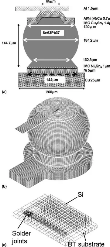
FIG. 1. (a) Schematic diagrams of the solder joint with Al Ni(V)/Cu UBM used in this study. (b) Three-dimensional view of the model in (a) with meshes contained in it.
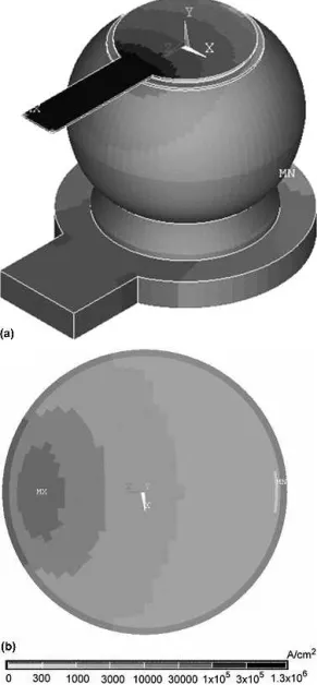
FIG. 2. Current density distribution in the solder joint with Al Ni(V)/ Cu UBM when powered by 0.567 A. (b) Cross-sectional view along the Z-axis of (a). Current crowding occurs in the entrance of the Al trace. The dotted lines show the six cross-sections examined in this study.
plays a critical role in the electromigration failure of the solder joints.10
Hence, increasing the electromigration resistance of the joints is an important and urgent issue. There are two approaches to increasing electromigration resistance: first, using a solder alloy that has better electromigration resistance; second, relieving the current crowding effect in solder joints by proper circuit or UBM design. For the former approach, Wu et al. developed a Pb-free solder alloy that has excellent electromigration resistance, close
to that of the high-Pb solder.11For the latter approach, it is expected that relieving the current crowding effect in solder joints would retard the formation rate of the voids and thus would increase the lifetime of the solder joints. However, no literature related to this issue has been reported so far. For this paper, we used finite element analysis to simulate the current density distribution of the solder joints with various structures of flip-chip solder joints. Possible solutions for the relieving current crowd-ing effect will be proposed.
TABLE II. Maximum current density and crowding ratios at different cross sections for the solder joint with the Al/Ni(V)/Cu thin film UBM.
Method Cross section Y1, UBM layer Y2, IMC layer
Y3, top layer of solder Y4, middle layer of solder Y5, necking layer of solder Y6, bottom layer of solder Standard Maximum 2.09 × 10⁵ 1.81 × 10⁵ 1.11 × 10⁵ 3.45 × 10³ 7.55 × 10³ 5.91 × 10³ Ratio 41.9 36.2 22.2 0.7 1.5 1.2
FIG. 3. Current density distribution in the different cross-sections: (a) cross-section Y1, located inside the UBM; (b) cross-section Y2, the IMC layer between the UBM and the solder; (c) cross-section Y3, the top layer of the solder connected to the IMC; (d) cross-section Y4, which has the largest diameter in the joint; (e) cross-section Y5, which has a smaller diameter due to the solder mask process; (f) cross-section Y6, which is situated at the bottom of the solder joint.
II. SIMULATION
The simulation model used in this study is schemati-cally shown in Fig. 1(a). Throughout this text, it will be denoted as the standard model. A thin film UBM of 0.4-m Al/0.3-m Ni(V)/0.4-m Cu was adopted for the chip side, and Ni metallization was used on the substrate side. Eutectic SnPb solder was adopted for the bump
materials. The Cu layer in the UBM was assumed to be completely consumed to form 1.4 m Cu6Sn5 IMC. Therefore, an effective layer of 0.7-m UBM with an effective resistivity of 29.54 ⍀ cm was used in the simulation model. On the substrate side, we assumed that 1 m Ni3Sn4 IMC was formed in the interface of the solder and the Ni metallization. Both Cu6Sn5and Ni3Sn4 IMCs were assumed to be the layered-type. The resistiv-ity and thermal conductivresistiv-ity values of the materials used in this simulation are listed in Table I. The model used in this study was SOLID69 8-node hexahedral coupled field element using Ansys simulation software (Ansys Inc., PA). For thermal simulation, we used an infrared micro-scope to measure the temperature in the solder bumps during current stressing12 and then adjusted the simula-tion parameters so that the simulated temperature in the solder matched the one measured by the infrared micro-scope under the same applied current. The three-dimensional (3D) schematic solder joint with meshes is shown in Fig. 1(b). The dimension of the mesh was 3.8m. The passivation and UBM openings are 85 and 120m in diameter, respectively. The contact opening on the substrate is 144m in diameter. The dimension of the Al trace is 34m wide and 1.5 m thick, whereas the Cu line on the substrate side is 80m wide and 25 m thick. A current of 0.567 A was applied from the Al trace, which drifted out of the bump from the Cu line. If one assumes the current drifts uniformly through the joint, the average current density in the Al trace was 1.11 × 10⁶
A/cm2
, and the calculated average current densities were 5.01 × 10³
and 3.48 × 10³ A/cm2
for the UBM opening of the chip side and the contact opening of the substrate side, respectively. Figure 1(c) shows the constructed model for thermal simulation, in which only two solder joints were stressed by current, as indicated by one of the arrows in the figure. The dimension of the Si chip was 7.0 × 4.8 mm and the thickness was 290m, whereas the dimension of the bismaleimide triazine (BT) substrate was 5.4 mm wide, 9.0 mm long, and 380m thick.
The current density distribution of the flip-chip solder joint was shown in Fig. 2(a). Current crowding is clearly observed in the vicinity of the entrance of the Al trace into the solder bump. However, it spreads out prior to reaching the half distance of the bump height, and there is no obvious current crowding at the bottom of the
TABLE III. Maximum current density and crowding ratios at different cross sections for the solder joint with larger passivation opening.
Method Cross section Y1, UBM layer Y2, IMC layer
Y3, top layer of solder Y4, middle layer of solder Y5, necking layer of solder Y6, bottom layer of solder Passivation opening: Maximum 2.33 × 10⁵ 2.03 × 10⁵ 1.22 × 10⁵ 3.67 × 10³ 8.16 × 10³ 6.04 × 10³
100m Ratio 46.6 40.6 24.4 0.7 1.6 1.2
FIG. 4. (a) 3D current density distribution in the solder joint with a larger passivation opening of 100m in diameter. (b) Current density distribution in the top layer of the solder (cross-section Y3) in (a).
solder bump. The cross-sectional view of Fig. 2(a) along the Z-axis is shown in Fig. 2(b). The current crowding effect can be clearly seen at the entrance of the Al trace. The maximum current density inside the solder is 1.11 × 10⁵
A/cm2
. In this paper, to evaluate the current crowding effect, we denote a “crowding ratio” as the local maxi-mum current density divided by the average current den-sity at the UBM opening. The average current denden-sity at the UBM opening is 5.01 × 10³
A/cm2
for the standard simulation model. Therefore, the corresponding crowd-ing ratio for the solder near the entrance is 22.2, which means that the local current density at the solder bump near the Al entrance is 22.2 times larger than the average value at the UBM opening. The larger the value is, the higher the current crowding effect.
To examine the current density distribution in various locations of the joint, six cross-sections were inspected. Their locations are shown in Fig. 2(b), in which cross-section Y1 is located inside the UBM layer, cross-cross-section Y2 represents the IMC layer, cross-section Y3 is located in the top layer of the solder joint connecting to the IMC, and cross-section Y4 is situated near the middle of the solder joint, which has the largest cross-section 184m in diameter. Cross-section Y5 is situated between the middle and the bottom of the solder, which has a necking due to the necessity of there being a solder mask, and cross-section Y6 represents the bottom of the solder joint close to the Ni3Sn4 IMC on the substrate side.
The current density distributions at the six cross sec-tions are shown in Figs. 3(a)–3(f). The current density distribution in the UBM layer is shown in Fig. 3(a), in which the maximum current density occurs near the Al entrance inside the passivation opening. The value reaches 2.09 × 10⁵
A/cm2
, and its crowding ratio is as high as 41.9. For the IMC layer shown in Fig. 3(b), the maximum value is 1.81 × 10⁵A/cm2, and the correspond-ing crowdcorrespond-ing ratio is 36.2. The maximum current density inside the solder occurs near the Al entrance inside the passivation opening, as shown in Fig. 3(c). The value reaches 1.11 × 10⁵A/cm2, and its crowding ratio remains as high as 22.2. For the remaining three layers, as shown in Figs. 3(d)–3(f), current distribution became more uniform, and thus the crowding ratios for the three layers were 0.7, 1.5, and 1.2, respectively. Therefore, changing the angle between the Al trace and the Cu conductor may not be able to alter the current density distribution. These results agreed with the thermal simu-lation results conducted by Lee et al.13 The maximum current density and the crowding ratios at different cross sections for the solder joint are listed in Table II. Since the top-layer of the solder (Y3 plane) is the most vulner-able location during current stressing, we will examine the current density distribution on this layer for the fol-lowing models that aim to relieve the current crowding effect.
FIG. 5. Current density distribution in the cross-section along the Z axis for (a) 0.7-m Cu UBM, (b) 5-m Cu UBM, and (c) 20-m Cu UBM.
III. METHODS FOR RELIEVING CURRENT CROWDING EFFECT
A. Effect of the dimension of the passivation opening
Figure 4(a) shows the 3D distribution of current den-sity in the solder bump with a larger passivation opening 100m in diameter. The cross-section area of the contact opening in this case is 1.4 times larger than that of
standard model. However, as seen in Fig. 4(a), current crowding still occurs in the vicinity of the Al entrance. Figure 4(b) shows the distribution of current density in the top layer of the solder. Surprisingly, its maximum current density increases up to 1.22 × 10⁵
A/cm2 , which is higher than 1.11 × 10⁵
A/cm2
for the standard model. This increase may be attributed to the decrease in bump resistance since the cross section of the bump became larger after the enlargement of the UBM opening.
TABLE IV. Maximum current density and crowding ratios at different cross sections for the solder joint with various thicknesses of Cu UBM.
Method Cross section Y1, UBM layer Y2, IMC layer Y3, top layer of solder Y4, middle layer of solder Y5, necking layer of solder Y6, bottom layer of solder UBM Cu thickness (m) 0.7 Maximum 2.58 × 10⁵ 2.36 × 10⁵ 1.17 × 10⁵ 4.07 × 10³ 8.23 × 10³ 6.10 × 10³
Ratio 51.5 47.1 23.4 0.8 1.6 1.2
5 Maximum 6.15 × 10⁵ 7.53 × 10⁴ 4.37 × 10⁴ 3.31 × 10³ 7.75 × 10³ 5.92 × 10³
Ratio 122.6 15.0 8.7 0.7 1.5 1.2
20 Maximum 1.55 × 10⁶ 1.27 × 10⁴ 7.54 × 10³ 3.04 × 10³ 7.71 × 10³ 5.78 × 10³
Ratio 309.2 2.5 1.5 0.6 1.5 1.2
FIG. 6. 3D current density distribution in the solder joint with different UBM resistivity values: (a) 295.4⍀ cm, (b) 1477 ⍀ cm, (c) 2954 ⍀ cm, and (d) 14770⍀ cm.
Table III lists the maximum current density and the cor-responding crowding ratio at cross sections Y1 to Y6 for this model. Hence, solder bumps with larger passivation opening have no effect on relieving the current crowding effect.
B. Effect of UBM thickness
To examine the effect of UBM thickness on the dis-tribution of current density, three thicknesses of Cu UBM were simulated, including 0.7, 5, and 20 m. Figures 5(a)–5(c) show the 3D distribution of current density in the solder joints for the three models, respec-tively. Although serious current crowding still occurs near the entrance of the Al trace for the three models, the solder bump is moved away from the crowding site due to the thicker UBM. The net effect is a lower maximum current density in the solder joint, and the current density inside the solder becomes more uniform. The maximum current density and the corresponding crowding ratio at
cross sections Y1 to Y6 for the three models are listed in Table IV. The maximum current densities in the top layer of the solder are 1.17 × 10⁵, 4.37 × 10⁴, and 7.54 × 10³
A/cm2
, respectively. It was surprising that the value dramatically decreased to 7.54 × 10³
A/cm2
for the solder joint with 20-m Cu UBM, which corresponds to a low crowding ratio of 1.5. Thus, the current crowding effect inside the solder bump was effectively relieved by add-ing a thick UBM, that is, by movadd-ing the UBM/solder interface away from the current crowding region. C. Effect of UBM resistivity
The best method of suppressing the current crowding effect in this study was to use a resistive UBM layer. In this simulation, we simulated four solder joints with 295, 1477, 2954, and 14770⍀ cm, which corresponded to 10, 50, 100, and 500 times the UBM resistivity of the standard model. Figures 6(a)–6(d) show the 3D distribu-tion of current density in the solder joint for the four models. It was found that the current density redistrib-uted in the contact opening. With the increase in UBM resistivity, a greater amount of current traveled further along the Al pad before flowing down into the contact opening. In addition, the current density distribution in the top layer of the solder became more uniform as UBM resistivity increased. Figure 7 shows the current density distribution inside the top layer of the solder along the Z axis. The current became uniformly distributed inside the solder layer, and maximum current densities ranged from 7.01 to 1.55 × 10⁴A/cm2. The corresponding crowding ratios are 14.0, 7.4, 5.4, and 3.1 for the solder joint with UBM resistivities of 295, 1477, 2954, and 14770⍀ cm, respectively, as listed in Table V. Furthermore, the cur-rent distribution in the UBM, IMC layers, and solder bump also became more uniform when highly resistive UBM layers were used.
Because the insertion of the resistive layers may in-crease the bump resistance and thus cause higher Joule heating in the solder joints, thermal simulation was per-formed to examine temperature distribution in the above
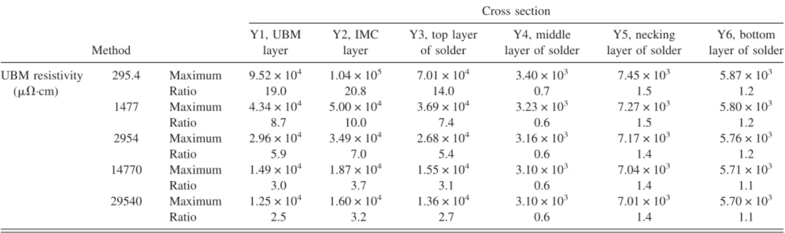
TABLE V. Maximum current density and crowding ratios at different cross sections for the solder joint with various UBM with high resistivities.
Method Cross section Y1, UBM layer Y2, IMC layer
Y3, top layer of solder Y4, middle layer of solder Y5, necking layer of solder Y6, bottom layer of solder UBM resistivity 295.4 Maximum 9.52 × 10⁴ 1.04 × 10⁵ 7.01 × 10⁴ 3.40 × 10³ 7.45 × 10³ 5.87 × 10³
(⍀·cm) Ratio 19.0 20.8 14.0 0.7 1.5 1.2 1477 Maximum 4.34 × 10⁴ 5.00 × 10⁴ 3.69 × 10⁴ 3.23 × 10³ 7.27 × 10³ 5.80 × 10³ Ratio 8.7 10.0 7.4 0.6 1.5 1.2 2954 Maximum 2.96 × 10⁴ 3.49 × 10⁴ 2.68 × 10⁴ 3.16 × 10³ 7.17 × 10³ 5.76 × 10³ Ratio 5.9 7.0 5.4 0.6 1.4 1.2 14770 Maximum 1.49 × 10⁴ 1.87 × 10⁴ 1.55 × 10⁴ 3.10 × 10³ 7.04 × 10³ 5.71 × 10³ Ratio 3.0 3.7 3.1 0.6 1.4 1.1 29540 Maximum 1.25 × 10⁴ 1.60 × 10⁴ 1.36 × 10⁴ 3.10 × 10³ 7.01 × 10³ 5.70 × 10³ Ratio 2.5 3.2 2.7 0.6 1.4 1.1
FIG. 7. Current density distribution inside the solder along the Z axis for the five UBM resistivity values at the top layer of the solder (cross-section Y3).
models. Figures 8(a)–8(e) show the temperature distribu-tions in the solder joints with 29.5 (standard model), 295, 1477, 2954, and 14770⍀·cm UBM, respectively. The solder joints were applied by 0.567 A, and the bottom of the BT substrate was maintained at 70 °C. For the stan-dard model in Fig. 8(a), the average temperature in the solder bump was 94.5 °C, which was obtained by aver-aging the temperatures in the white dotted line in the figure. The solder near the entrance area of the Al trace has higher temperature of 98.8 °C. As the resistivity of the UBM increased, Joule heating effect became signifi-cant, as shown in Figures 8(b)–8(e). The temperature in-crease due to Joule heating was as large as 30.7 °C for the solder joint with 14770⍀ cm UBM. However, the
current flowing in the solder joints is generally less than 0.2 A during device operation. Figure 8(f) shows the temperatures in the solder joints as a function of applied current up to 0.567 A. It is found that Joule heating effect was not serious under 0.2 A. For the standard model, the temperature increase was 2.2 °C, whereas it was 2.8 °C for the solder joint with 14770⍀ cm UBM. This indi-cates that the temperature increase due to the resistive UBM was only 0.6 °C at 0.2 A.
IV. DISCUSSION
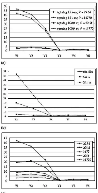
Figures 9(a)–9(c) depict the crowding ratios at cross sections Y1 to Y6 for the above four methods. It is clear
FIG. 8. Temperature distribution in the solder bumps when stressed by 0.567 A: (a) standard model, (b) solder joint with resistive UBM of 295.4⍀⭈cm, (c) solder joint with resistive UBM of 1477 ⍀⭈cm, (d) solder joint with resistive UBM of 2954 ⍀⭈cm, (e) solder joint with resistive UBM of 14770⍀⭈cm, and (f) simulated temperature in the solder joint as a function of applied current up to 0.567 A.
that there is no effect on relieving current crowding by the enlargement of the passivation opening, as shown in Fig. 9(a). A thicker Cu UBM can relieve current crowd-ing in the solder bump by movcrowd-ing the UBM/solder in-terface away from the current crowding region, as seen in Fig. 9(b). The thicker the UBM is, the less the current crowding effect. Figure 9(c) shows that the crowding ra-tios in the solder joint can be lowered to 3.1 through use of more resistant UBM. This UBM layer can suppress current crowding at the UBM/solder interface.
The best methods for relieving the current crowding effect inside the solder bump fall into two categories:
(i) moving the UBM/solder interface away from the cur-rent crowding region, and (ii) suppressing curcur-rent crowd-ing at the UBM/solder interface. If the UBM/solder in-terface can be moved away from the current crowding region, the threat from the high current density can be avoided. As shown in Figs. 6(a)–6(c), one can clearly see that the current density drops very rapidly when it is moved way from the chip side. Therefore, if one in-creases the thickness of UBM, the current crowding re-gion will locate within the UBM, and therefore, the UBM/solder interface will be further away from it. Thick Cu UBM has been adopted for use in the flip-chip solder joints.14Thus, it is expected the joints would have better electromigration resistance.
To suppress the current crowding effect, the best sce-nario would be to have the current flowing though the whole solder uniformly. To achieve this goal, increasing the resistivity of UBM would be the best method. Our simulation shows that the current crowding ratio can be reduced to 3.1 when the UBM resistivity is increased to 4770⍀ cm. However, the tradeoff is the increase in the resistance of the solder joint. The vertical resistance of the standard model was estimated to be 1.2 m⍀. The total resistances of the solder joint became 1.4, 2.1, 3.0, and 10.3 m⍀ for the solder joints with a UBM resistivity of 295, 1477, 2954, and 14770⍀ cm, respectively. This resistive layer could be a TiN, TaN, or Ta material, and could be deposited with UBM, or it could be an addi-tional layer between the Al pad and the UBM. Further-more, our thermal simulation shows that the Joule heat-ing effect due to the resistive layers was less than 0.6 °C when the applied current was less than 0.2 A. Therefore, the insertion of the resistive layers could relieve current crowding effect significantly and cause very small Joule heating effect at low applied current. Nevertheless, it is still unknown if it is compatible with the current flip-chip manufacturing process, and thus it requires further ex-perimental study.
Furthermore, one can use the hybrid of the above ap-proaches to relieve the current crowding effect. If one adopts the highly resistant layer to relieve the current crowding effect, increasing the cross-section of the pas-sivation opening would have a further effect in reducing the maximum current density in the solder bump. When the model in Sec. III. B is used with a larger passivation opening and the high resistivity UBM of 14770⍀ cm is adopted, the maximum current density can be further reduced down from 1.6 × 10⁴ to 1.3 × 10⁴A/cm2.
V. CONCLUSIONS
A three-dimensional simulation was used to demon-strate that current crowding in the solder joints can be successfully suppressed either by thick Cu UBM or a highly resistive UBM layer. The crowding ratio in the
FIG. 9. The crowding ratios for the Y1 to Y6 cross-sections for (a) effect of dimension of passivation opening, (b) effect of Cu UBM thickness, and (c) effect of UBM resistance. It shows that the current crowding effect can be successfully relieved in the solder joints with a thick Cu UBM or with the highly resistive UBM.
solder can be reduced from 23.4 to 1.5 when a 20-m Cu UBM is used, and it can be diminished to 3.1 when a 0.7-m UBM of 14770 ⍀ cm in resistivity is adopted. In addition, the current crowding effect could not be relieved merely by increasing the diameter of the passi-vation opening or changing the angle between the Al trace and the Cu line. The solder joints with a lower crowding ratio were expected to have better electromi-gration resistance, and experimental data are needed to verify the simulation results.
ACKNOWLEDGMENTS
The authors would like to thank the National Science Council of the Republic of China for financial support through Grant No. 92-2216-E-009-008. In addition, the assistance of the simulation facility from the National Center for High-performance Computing (NCHC) in Taiwan is appreciated.
REFERENCES
1. R. Glenn: Blackwell, The Electronic Packaging Handbook, CRC Press in cooperation with IEEE Press, Boca Raton, FL (2000). 2. The International Technology Roadmap for Semiconductor
(Semi-conductor Industry Association, San Jose, CA, 2003).
3. K.N. Tu: Recent advances on electromigration in very-large-scale-integration of interconnects, J. Appl. Phys. 94, 5451 (2003). 4. S. Brandenburg and S. Yeh: Electromigration studies of flip chip
bump solder joints, in Proceedings of Surface Mount International
Conference and Exhibition, San Jose, CA (SMTA, Edina MN 1998), p. 337.
5. C.Y. Liu, C. Chen, C.N. Liao, and K.N. Tu: Microstructure-electromigration correlation in a thin strips of eutectic SnPb solder stressed between Cu electrodes. Appl. Phys. Lett. 75, 58 (1999). 6. P.S. Ho and T. Kwok: Electromigration in metals, Rep. Prog.
Phys. 52, 301 (1989).
7. C.K. Hu and J.M.E. Harper: Copper interconnections and reliabil-ity. Mater. Chem. Phys. 52, 5 (1998).
8. E.C.C. Yeh, W.J. Choi, and K.N. Tu: Current-crowding-induced electromigration failure in flip chip solder joints. Appl. Phys. Lett.
80(4), 580 (2002).
9. W.J. Choi, ECC. Yeh, and K.N. Tu: Mean-time-to-failure study of flip chip solder joints on Cu/Ni(V)/Al thin-film under-bump-metallization. J. Appl. Phys. 94, 5665 (2003).
10. J.W. Nah, K.W. Paik, and J.O. Suh: Mechanism of electromigra-tion-induced failure in the 97Pb–3Sn and 37Pb–63Sn composite solder joints. J. Appl. Phys. 94, 7560 (2003).
11. J.D. Wu, C.W. Lee, P.J. Zheng, J.C.B. Lee, and S. Li: Electromi-gration reliability of SnAgxCuyflip chip interconnects, in 2004
Electronic Components and Technology Conference, (IEEE, New York) p. 961.
12. T.L. Shao, S.H. Chiu, C. Chen, D.J. Yao, and C.Y. Hsu: J. Elec-tron. Mater. 33, 1350 (2004).
13. T.Y. Tom Lee, T.Y. Lee, and K.N. Tu: A study of electromigra-tion in 3D flip chip solder joint using numerical simulaelectromigra-tion of heat flux and current density, in Proceedings of the 51th Electronic Components and Technology Conference, Packaging, and Manu-facturing Technology Society, (2001), p. 558.
14. J.W. Jang, L.N. Ramanathan, J.K. Lin, and D.R. Frear: Spalling of Cu3Sn intermetallics in high-lead 95Pb5Sn solder bumps on Cu
under bump metallization during solid-state annealing. J. Appl. Phys. 95, 8286 (2004).