. ... ~: :: ::::i ~#:.i.~'~:i~ :%~!:i:::::..:..::.-...
applied
surface science
ELSEVIER Applied Surface Science 102 (1996) 404-407
Atomic force microscopy study on the surface structure of
oxidized porous silicon
T.F. Y o u n g a,*, I.W. H u a n g a Y.L. Y a n g a W.C. K u o a I.M. Jiang a T.C. C h a n g b
C.Y. C h a n g b
a Department of Physics, National Sun Yat-sen University, Kaohsiung 80424, Taiwan, ROC
b National Nano Device Laboratory and Institute of Electronics, National Chiao-Tung University, Hsinchu 30050, Taiwan, ROC
Abstract
We study the surface structure of porous silicon (PS) using atomic force microscopy (AFM), before and after oxidation in a HNO 3 solution. The AFM image shows the PS surface with a self-affine random fractal structure of wires, hillocks and voids in various scales. After oxidization the wires and hillocks of PS structures are glazed with oxide and the voids are filled. PS structure is altered to a simple self-affine fractal structure of hillock clusters. The fractal dimension D of PS is around 2.3, which decreases with increasing oxidization to about 2.0 of a smooth surface for the saturated oxidization. Our direct observation of the fractal structure of PS from AFM data reveals a good explanation for the recently found novel nonlinear dc-response in Ag thin films deposited on PS. We find the fractal surface structure of oxidized PS responds to the stepwise avalanche electric breakdown of the resistivity of Ag thin films deposited on oxidized PS.
Since the first report [1] o f the strong visible r o o m temperature photoluminescence (PL) o f porous sili- con, m a n y investigations have been devoted to real- izing its optoelectronic applications. The transport properties o f metal thin film contacting on PS is important from both fundamental and technological points o f view. Recently the m o r p h o l o g y structure o f the PS rough surface has been studied extensively. Obviously, the surface m o r p h o l o g y o f PS has an important influence on its PL. Furthermore, the oxi- dation procedure can i m p r o v e the P L stability and uniformity o f PS [2-4]. The oxidized surface mor- p h o l o g y o f PS has also been intensively studied
* Corresponding author. TeL: + 886-7-5327027; fax: +886-7- 5310546; e-mail: [email protected].
[3--5]. The p h e n o m e n o n o f PS formation had been discussed by Smith et al. before [6-8]. They sug- gested a fractal structure o f the PS formation. Very recently, R o y and S o o d [9] simulated the PS surface m o r p h o l o g y with the diffusion-limited aggregation scheme, and Mattai et al. [10] p e r f o r m e d an experi- mental study by R a m a n scattering. Their results show PS exhibiting the fractal structure. Recently we have measured the dc-response o f A g thin films deposited on PS [11]° A nonlinear dc-conductivity o f the A g thin films deposited on PS was found. Furthermore, after the PS sample is oxidized in H N O 3 solution, the nonlinear dc-resistance o f A g thin films exhibits a fractal-like property depending on the PS structure. A n d we p r o p o s e d a branched Koch curve fractal m o d e l to explain the novel electric transport phe- n o m e n a [12]. A c c o r d i n g to our model, the nonlinear 0169-4332/96/$15.00 Copyright © 1996 Elsevier Science B.V. All rights reserved.
T.F. Young et al. /Applied Surface Science 102 (1996) 404-407 4 0 5
dc-response m a y be explained with a fractal-like network of the A g thin film deposited on PS surface. For a detailed understanding of this fractal-like phe- nomena, we further study the PS surface structure with AFM, which reveals detailed, three dimensional images of PS surface topography. And the A F M data does reveal a self-affine fractal structure of PS sur- face, which m a y correspond to the novel dc-response o f A g thin films deposited on oxidized PS.
In this work the PS sample is fabricated by an- odization o f the p-type boron doped (100) single- crystal Si with resistivity of 5 - 8 ~ cm. Aluminum ohmic contacts are made on the backside of PS before electro-chemical etching. The anodization is performed by a constant current of 10 m A / c m 2 in the electrolyte of H F / C z H s O H = 1:1 solution at 30°C for 8 s to 30 min. W e oxidize PS by immersing samples in H N O 3 acid with the concentration from 0.1 M to 1 M, and for 1 to 10 min. Before and after oxidation, all PS samples are monitored using a transmission Fourier transform infrared spectroscopy (FTIR) ( B o m e m 150 series). The morphology of PS surface, before and after oxidation, is imaged by A F M (Digital Instruments, NanoScope III) in contact mode with a commercial silicon nitride tip of radius about 30 nm. For some PS samples contaminated by particles, A F M images are taken with a tapping mode instead. With the A F M software (Digital In- struments) the surface roughness profiles are ana- lyzed in terms of a 'fractal dimension' D which is referred to as fractal-based roughness [13]. D in- creases with the roughness of the surface. The method for determining D involves the use of a box dimen- sion: Through the box counting the fractal dimension D is defined in terms of N oc b -D. In brief, this method overlays a profilometer curve with a uniform grid or a set o f ' b o x e s ' of side length, b, and a count is made o f the nonempty boxes, N. The box size b is changed and the count is repeated. Finally, the counts are plotted against each box size on a l o g - l o g scale to obtain a boxcount plot, and the slop of the least- squares-fit line o f the resulting curve gives the frac- tal dimension. The analyzation o f surface roughness profiles using fractal theory has been illustrated an advantage in characterizing the surface complexity [13,14].
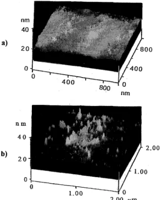
Fig. la and b present the A F M images o f as anodized PS for 8 s and 30 min. In Fig. la the
a)
nlTI 40 20 90 t l O 0 - n r n r i mb)
4 0 2 0 ¸ 2 . 0 0 2.00 ~mFig. 1. Three-dimensional AFM image of the as anodized porous silicon surface structure formed on p-type (5-8 ~, (100)) Si, 1 = 10 mA/cm 2 for: (a) t = 8 s and (b) t = 30 min. The PS layer thickness and roughness are not monotonically proportional to the anodizafion time.
shallow hillocks have just formed a cluster-like sur- face in this early anodization phase. As the anodiza- tion time increases, the PS surface layer becomes thicker and rougher. However, the thickness and roughness of PS are not monotonically increased with the anodization time. The wires and hillocks of the PS are continuously removed and new ones will start to form. In Fig. l b shows the 30 rain as anodized PS with a thickness of only ~ 40 nm. This figure displays similar hillock structures in large and small scales, which manifests self-affine fractal. The morphology of as anodized PS is strongly dependent on doping, conductivity [6], and on the anodization conditions [3], such as current density, irradiation o f the light, etc. The influence on the morphology is due to the electro-chemical etching reactions in which the corrosion and diffusion take place between the PS surface layer and the electrolyte. The transport processes such as surface diffusion, charge migration
406 T.F. Young et al. /Applied Surface Science 102 (1996) 404-407
in bulk, and convection, also have great impact on the texture of the PS layer. This work concerns the AFM analysis on the oxidized PS surface.
Fig. 2a and b show AFM images of 5 min an- odized PS with light and saturated oxidizations, re- spectively. Fig. 2a displays a self-affine structure, too. This PS layer is much thicker than that of the 30 rain anodized (Fig. lb). We observe AFM pho- tographs with different fractal structures in the PS surface which varied throughout the oxidization pro- cedure. In Fig. 2b the AFM image shows the PS forming big oxide clusters after saturated oxidation. The structures of oxidized PS, the wires and hillocks, are glazed with oxide and the voids also are filled. And the PS structure changes to simpler fractal hillock clusters. Its fractal dimension D is nearly 2.0, just like a smooth surface. To demonstrate the self-affine fractal feature AFM images are taken of one PS sample, of 20 min anodized and 10 min oxidized in 1,/8 M HNO 3, in two scales. Fig. 3a
a m 300 a ) 200 100 £ 5 . 0 0 p-m 5.00 hi3 200 b) ~oo ~ . . , o , v 5.00 .am 5.00
Fig. 2. AFM photograph of the 5 min anodized porous silicon and oxidized for: (a) in 1 / 8 M HNO 3 for 3 min, (b) in 1 M HNO 3 for 10 min.
a)
nil" 500 250 0 ,5.005.00 #m
n m 2 0 . 0 b) loo 10.0 J u 1 0 0 ~ n mFig. 3. (a) AFM photograph of the 20 min anodized porous silicon oxidized in 1 / 4 M HNO 3 for 3 min. (b) Higher resolution AFM image of the same sample as in (a).
shows the PS structure in 5 /zm × 5 /xm area and Fig. 3b in 0.1 /xm × 0.1 /xm area. The smallest PS wire we can see is about 5 nm wide in Fig. 3b. They show self-affine structures and have the same fractal dimension.
All samples show fractal structures. In measuring their fractal dimension, we find they have different values. The fractal dimension D determines the rela- tive amounts of the surface irregularities at different distance scales. The fractal dimension D is around 2.3 for the as anodized and lightly oxidized PS. The maxima of fractal dimensions occur at the medium range of the oxidization for different anodization times. The PS surface of saturated oxidization is very smooth with a fractal dimension approaching D = 2.0 (in Fig. 2b). In spite of different structures of as anodized PS surface, the PS samples, after oxidiza- tion, acquire similar fractal structures with the fractal dimensions D = 2.0 for saturately oxidized PS sam- ples. That can be understood with the AFM images, since after oxidization the wires and hillocks of PS
T.F. Young et al. /Applied Surface Science 102 (1996) 404-407 407 structures are glazed with oxide and the voids are
filled. A further study o f the correlation among the PS structure feature, roughness, and anodization con- ditions is still in progress.
The A F M data is consistent with earlier proposed branched Koch curve structure model for dc-conduc- tivity of the Ag thin films deposited on PS. W e proposed the conductivity due to the percolation of Ag conducting particles or clusters and the t u n n e l i n g effect among the clusters in Ag thin film under an influence of fractal nature of the PS surface struc- ture. The total resistance of Ag thin film is formed by connecting the resistor in series. W h e n PS is oxidized, the fractal structure is smoothed to forming simpler fractal clusters. Therefore, the electrical path of Ag film on PS surface can be simplified with the branched Koch curve [12].
In summary, in this A F M study on the oxidized PS structure, the A F M data reveals a fractal structure of the surface layer for as anodized and oxidized PS. After oxidation in H N O 3, the PS surface is reduced to a simpler fractal structure. In a higher resolution A F M image we observe a self-affine fractal feature. The A F M data is consistent with our earlier pro- posed branched Koch curve fractal model for the dc fractal-like response of Ag thin films deposited on PS. The fractal dimension is around D = 2.3 for as anodized and lightly oxidized PS, and exhibits a m a x i m u m in m e d i u m oxidization range. A n d for saturately oxidized PS the fractal dimension approxi- mates D = 2.0, which can be explained by the A F M data.
Acknowledgements
W e wish to thank Professor M.K. Lee and Profes- sor C. Chou for their helpful assistance. This work was supported by the National Science Council of ROC under contract No. NSC 84-2112-Ml10-006.
References
[1] L.T. Canham, Appl. Phys. Lett. 57 (1990) 1046.
[2] P. O'Keeffe, Y. Aoyagi, S. Komuro, T. Kato and T. Morikawa, Appl. Phys. Lett. 66 (1995) 836.
[3] R. Sabet-Dariani and D. Haneman, J. Appl. Phys. 76 (1994) 1346.
[4] F.L. Zhang, X.Y. Hou, M. Yang, D.M. Huang and X. Wang, Acta Phys. Sin. 43 (1994) 499.
[5] L. Tsybeskov and P.M. Fauchet, Appl. Phys. Lett. 64 (1994) 1983.
[6] R.L. Smith and S.D. Collins, J. Appl. Phys. 71(8) (1992) R1. [7] S.F. Chuang, S.D. Collins and R.L. Smith, Appl. Phys. Lett.
55 (1989) 1540.
[8] R.L. Smith, S.F. Chuang and S.D. Collins, J. Electron. Mater. 17 (1988) 533.
[91 A. Roy and A.K. Sood, Solid State Commun. 93 (1995) 995. [10] C.C. Mattai, J. Grvartin and A.A. Cafolla, Thin Solid Films
255 (1995) 174.
[11] T.F. Young, J.F. Liu, C.C. Wu, G.H. Fu and C.S. Chen, Appl. Surf. Sci. 92 (1996) 57.
[12] T.F. Young, W.C. Kuo, I.M. Jiang, T.C. Chang and C.Y. Chang, Physica A 221 (1995) 380.
[13] S. Chesters, H.Y. Wen, M. Lundin and G. Kasper, Appl. Surf. Sci. 40 (1989) 185.
[14] B.B. Mandelbrot, in: Fractals in Physics, Proc. 6th Trieste Int. Symp., Eds. L. Pietronero and E. Tosatti (Elsevier, New York, 1986)p. 10.