This content has been downloaded from IOPscience. Please scroll down to see the full text.
Download details:
IP Address: 193.106.31.54
This content was downloaded on 25/06/2016 at 13:03
Please note that terms and conditions apply.
View the table of contents for this issue, or go to the journal homepage for more 2016 J. Phys.: Conf. Ser. 682 012009
Chemical vapour deposition growth and Raman
characterization of graphene layers and carbon nanotubes
Y-C Lai1, P M Rafailov2,5, E Vlaikova2, V Marinova1,3, S H Lin4, P Yu1, S-C Yu1,
G C Chi1, D Dimitrov2,3, P Sveshtarov2 V Mehandjiev2 and M M Gospodinov2
1Department of Photonics, National Chiao Tung University, Hsinchu 30010, Taiwan 2 Institute of Solid State Physics, BAS, 72 Tzarigradsko Chaussee blvd., 1784 Sofia,
Bulgaria
3Institute of Optical Materials and Technologies, BAS, Sofia 1113, Bulgaria 4Department of Electrophysics, National Chiao Tung University, Hsinchu 30010,
Taiwan
E-mail: [email protected]
Abstract. Single-layer graphene films were grown by chemical vapour deposition (CVD) on
Cu foil. The CVD process was complemented by plasma enhancement to grow also vertically aligned multiwalled carbon nanotubes using Ni nanoparticles as catalyst. The obtained samples were characterized by Raman spectroscopy analysis. Nature of defects in the samples and optimal growth conditions leading to achieve high quality of graphene and carbon nanotubes are discussed.
1. Introduction
Graphene, due to its outstanding properties as high electrical mobility [1], high thermal conductivity [2] and exceptionally low absorbance [3] play a key role in scientific and technological development. Up-to-date application of graphene in integrated devices requires wafer scale deposition technology with controllable number of graphene layers. On the other hand, the implementation of graphene as transparent conductor needs reproducible deposition of single or few layers. Especially, synthesis of bilayer graphene becomes increasingly desirable as it was reported to develop a tuneable band gap upon mechanical stress and electrical gating [4]. Among the well-known methods of graphene growth as mechanical exfoliation (characterized with very low concentration of structural defects, however with limited industrial applications due to the lack of thickness, size and location control), chemical vapor deposition (CVD) turns out to be the most prospective, inexpensive and readily accessible approach to satisfy the complex requirements of optoelectronics and microelectronics for large-area, high-quality graphene with low-density of structural defects.
During the CVD process, transition metals as Cu, Ni, Fe, play a fundamental role in reducing the decomposition temperature of methane [5]. One essential limitation of utilizing Ni as deposition substrate is that single- and few-layered graphene is obtained only over few-micron regions and the film is not homogeneous and with no uniform thickness over the entire substrate. The impossibility to control the number of layers is partially due to the fact that the segregation of carbon from the metal carbide upon cooling occurs rapidly within the Ni grains and heterogeneously at the grain boundaries
[6]. In contrast, the peculiar combination of very low affinity between carbon and copper combined with the ability to form transient soft bonds facilitates formation of nucleation sites on the copper foil surface that form preferentially single-layer graphene through lateral growth [5]. In that aspect Cu is the perfect candidate for making large area, single layer graphene films with uniform thickness due to the low solubility of carbon in Cu.
In this work we study CVD growth of graphene on copper foil as well as the plasma-enhanced CVD growth of carbon nanotubes. We characterize the obtained samples with Raman spectroscopy and discuss some consequences of the transfer of graphene layers on Si wafers.
2.
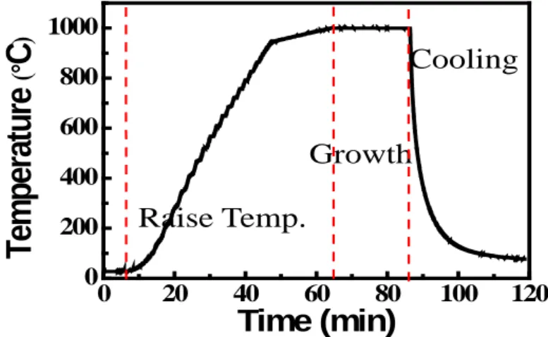
ExperimentalThe graphene samples were grown in quartz tube furnace by a CVD method involving high purity methane (99.9995%) and hydrogen gases. The growth procedure is displayed in figure 1. Under vacuum of 270 mTorr, the furnace is heated with 50 sccm flow of H2. When temperature is stabilized
at 1000oC, the hydrogen flux is decreased to 20 sccm and methane is introduced into the tube while
keeping the pressure around 630 mTorr to grow graphene for 20 min. Rapid cooling is then applied after growth, and methane and hydrogen gas flows are continued throughout the cooling process until the temperature falls below 200oC.
Raise Temp.
Growth
Cooling
0 20 40 60 80 100 120 0 200 400 600 800 1000T
em
p
er
at
u
re
(°
C
)
Time (min)
Figure 1. Stages of the graphene growth procedure.
To transfer the obtained graphene we used a spin coater to deposit photoresist PMMA (A4) on the top of the graphene layer to mechanically support graphene after copper is etched away. Fe(NO3)3.9H2O was used as copper etchant. The PMMA/graphene/Cu foil was put to float in the
etchant solution to selectively etch out the Cu-foil. Afterwards the obtained the PMMA/graphene layer was rinsed several times with doubly ionized water and transferred to a SiO2/Si substrate, followed by
removal of the PMMA using hot acetone.
Carbon nanotubes were grown in an Oxford Instruments Plasmalab 100 reactor from C2H2 gas
precursor in a mix of Ar and H2 as carrier and NH3 as additional radical source (gas purity 99.999 %)
at a temperature in the range 800–950 C at chamber pressure 1.5 Torr. The NH3:CH4:H2 ratio was
maintained constant at 10:3:20 by mass-flow controllers regardless of the chamber total pressure. The chamber features a hot table consisting of a meandered sheet metallic heater and graphite susceptor Ceramic heat shields around the hot plate were used to reflect emitted radiation thus reducing heating power loss. The gas mixture entered the reaction space through a showerhead. Capacitively coupled RF (13.56 MHz) plasma was ignited between the showerhead and the grounded hot table both in the pretreatment and the growth step. Some of the chamber construction details, the substrate holder and the high temperature furnace arrangement are shown in the figures. The substrates were semiconductor
silicon wafers coated with TiN diffusion barrier and 5 nm Ni catalyst film. The latter was activated by plasma treatment at the growth temperature in a predeposition step.
The Raman spectra were measured on a Jobin Yvon Labram spectrometer with a CCD detector and entrance slits set to 1.5 cm−1 spectral width. The 632.8 nm line of a He/Ne-laser and the 488 nm line of an Ar+ laser were used for excitation, the absolute accuracy being 1 - 2 cm−1. The laser beam with
power not surpassing 0.5 mW was focused on a spot of about 1 - 2 μm in diameter on the sample surface using microscope optics with an objective of x50 magnification.
Electrical measurements for determination of the carrier mobility were performed by means of silver-paste contacts.
3.
Results and Discussion3.1. Growth and characterization of graphene
The Raman spectrum of graphene and carbon nanotubes has several unique features [7,8]. The G-band at around 1580 cm−1 arises from an E2g zone-center vibration of the sp2 -hybridized carbon network.
The D-band is a double-resonant (DR) defect-induced feature arising from a breathing-like vibration at the Brillouin zone boundary (K point) [9]. Its frequency is excitation-energy dependent and normally varies in the interval 1320 – 1360 cm−1 for visible laser energies. The 2D band is the second order of the D band and is also excitation-energy dependent. Since momentum conservation is provided by two phonons with opposite wave vectors, no defects are required for the DR activation process of the 2D band. Thus the intensity ratio I(D)/I(2D) of the D band and the 2D band is proportional to the amount of structural defects. Another DR defect-induced feature is the D’ mode (≈1620 cm−1) involving
vibrations near the Γ point. Combination modes of graphene in the intermediate frequency range are the so-called M-band at ≈1750 cm−1 (absent in single-layer and twisted (non-AB-stacked) double-layer graphene) and a doublet between 1800 and 2100 cm−1 [10]. The defect-induced combination mode of the D and D’ band appears at ≈ 2920 cm−1.[8] Around 2450 cm−1 there is another characteristic band
for graphene-based materials denoted as G* which arises from the combination mode of iTO phonons and longitudinal acoustical (LA) phonons [8]. Finally, non-dispersive bands activated by the mutual perturbation of adjacent layers in twisted double-layer graphene, called the I-band were reported recently to lie on the higher-energetic side of the D-band [11], and may facilitate distinguishing the AB-stacked bilayer graphene from the twisted one [12].
Figure 2. Optical micrograph of the obtained
graphene film after transfer on Si/SiO2.
In the Raman spectrum of graphene, the ratio between the intensity of the G band and the 2D band (I(G)/I(2D)), the lineshape of the 2D band and its width (FWHM) can be used as a measure for the number of single-atomic layers as the 2D band has characteristic lineshapes for mono- and bi-layer graphene, due to differences in their electronic structure [7,8]. In characterising single-layer graphene
(SLG) and discriminating between it and the various kinds of bilayer graphene (BLG) we consider the 2D peak frequency the most important parameter as it blue-shifted [13] with respect to that of SLG for any arbitrary twisting angle between the two layers of BLG [14]. On the other hand, a 2D peak with single-Lorentzian shape of BLG was found to be in some cases even narrower than that of SLG [14]. In the following analysis we will use also the second-order modes for additional confirmation of our conclusions.
Figure 2 shows an optical microscope image of the obtained graphene transferred from the Cu foil to Si/SiO2. Obviously, there are highly uniform regions with size of several tens of μm2 without any
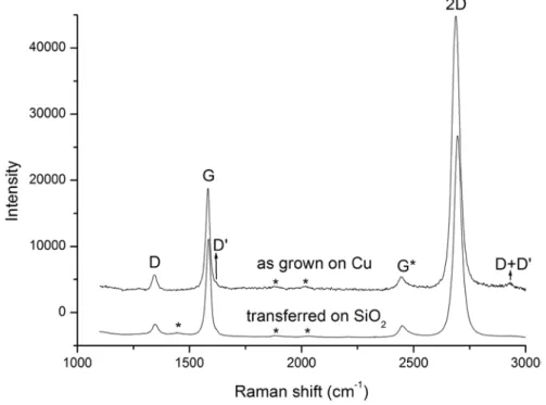
visible change in contrast. To investigate the quality and proof the visible homogeneity of the synthesized graphene films spot-resolved Raman measurements were performed over those regions. Figure 3 shows representative Raman spectra of the obtained graphene both as grown on Cu foil and transferred onto SiO2/Si substrate excited at 2.54 eV.
Figure 3. Raman spectra of the obtained graphene film recorded “as grown”
and after transfer onto Si/SiO2 as marked in the figure. Asterisks mark
important intermediate bands: the doublet between 1800 and 2100 cm−1 and the probable superlattice feature at ≈ 1375 cm−1. To enable reliable comparison the spectra are normalized to the same G-band intensity.
The obtained graphene exhibits FWHM (2D) of 37 cm−1 and I(2D)/I(G) ~ 2.5. Low-intense but well-formed defect-induced bands (I(D)/I(G) < 0.05) are observed. The 2D lineshape is fitted with a single Lorentzian centered around 2690 cm−1. These findings indicate SLG with few defects [15]. Surprisingly, the transfer onto SiO2/Si seems to diminish the amount of structural defects as the defect-induced modes D, D’ and D+D’ are weaker after transfer (see figure 3). On the other hand, transfer onto SiO2/Si probably leads to partial overlap and creation of folded BLG. This is indicated by
the blue-shift (5 – 10 cm−1) of the 2D band and decrease of the I(G)/I(2D) ratio after transfer as well as by the appearance of a new band around 1450 cm−1, which falls in the region of appearance of perturbation-induced bands, indicative of bilayer superlattice structures [12]. Examination of the combination modes in figure 3 confirms the presence of SLG. The asymmetric shape of the excitation-energy dependent D* band is typical for single-layer graphene [16]. The M-band at ≈1750 cm−1 is
completely absent in all spectra and shape and frequency of the doublet between 1800 and 2100 cm−1 are characteristic for SLG Raman spectra excited at 488 nm [10].
The 2D band blue shift could also be due to PMMA-residues from the transfer process that usually turns graphene into p-type doping [17]. The lack of large doping-induced shift of the G-band above 1586 and the sufficiently high I(2D)/I(G) ratio [18,19] in all spectra, however, give us confidence that the doping level of our samples, if any, is sufficiently low. Likewise, the lack of strain-induced changes in the shape of the G- and 2D band shows that possible transfer-induced wrinkles are below detectable limit. These additional arguments are important as both charged impurities and strain do not contribute to the D band [8] and their influence cannot be assessed from the D band intensity.
The sheet resistance of the obtained graphene was established to be 1810 Ω/sq with a carrier mobility slightly over 1000 cm2/Vs. The high resistance value is not surprising if one takes into
account the contact resistance to the silver paste and the polycrystallinity of the graphene layer. Sheet resistance of similar-quality graphene measured via thermally evaporated gold electrodes [20] was found to barely surpass 1000 Ω/sq. This gives us confidence that the intrinsic sheet resistance of the obtained graphene is of the order of several hundreds Ω/sq which makes it suitable for application as transparent conductor in optoelectronics.
3.2. Growth and characterization of carbon nanotubes
Vertically aligned carbon nanotubes were grown on Ni/TiN/Si substrates from acetylene precursor after catalyst nanoparticles activation in hydrogen plasma [21]. Growth occurs via carbon species adsorption, surface migration and trapping at atomic steps at the Ni nanoparticles’ surface. The growing nanotube detaches from the substrate the catalytic particle which stays at the nanotube tip and to a large extent defines the nanotube diameter. Tube growth terminates when all the catalytic particle surface gets completely covered with a crust of fixed non-mobile carbon species. NH3 provides cyano–
containing radicals in the plasma which combine with acetylene–derived species to produce the carbon source at the catalytic seed surface thus lowering the needed free energy change. The RF electric field provides orienting force that keeps top-seeded growth morphologically stable. This produces straight nanotubes aligned perpendicular to the substrate. Scanning electron microscopy (not shown) identified all nanotubes to be multi-walled and therefore of metallic nature with a length of about 1.2 µm.
Figure 4 displays representative Raman spectra of the obtained carbon nanotubes. The spectra exhibit the typical Raman features of multiwalled carbon nanotubes. The high intensity of the double resonant defect-dependent bands D and D’ points to a considerable amount of defects. This is, however, typical for multiwalled carbon nanotubes which contain a lot of incommensurate structures. Furthermore, the intensity ratio I(D)/I(2D), though varying over the sample, remains below unity indicating that the honeycomb lattice of the distinct walls is not deteriorated by the defects.
4.
ConclusionSingle-layer graphene films were grown on Cu foil substrates by low-pressure chemical vapour deposition. Raman characterization of the obtained Cu layers reveals single-crystal graphene with little amount of defects and good homogeneity. We observe spectroscopic indication for small fraction of bilayer graphene on the sample transferred onto silicon and explain this with a possible partial folding during the transfer process. The spectroscopic characterization and the assessment of the electrical properties reveal good-quality graphene suitable for application as transparent conductor in hybrid optoelectronic structures. Straight aligned perpendicular to the substrate carbon nanotubes were grown by plasma-enhanced chemical vapour deposition and characterized with Raman spectroscopy. The majority of them are multi-walled and therefore of metallic nature.
5.
AcknowledgementsThe authors acknowledge support from the FP7 Project INERA 316309 with the EU. This work was funded by the Bulgarian Science Fund under the project DFNI-T02/26 and the Ministry of Science and Technology (MOST), Taiwan under the contracts: MOST 104-2221-E-009-164; and 103-2911-I-009-516.
6. References
[1] Neto A H C, Guinea F, Peres N M R, Novoselov K S and Geim A K 2009 Rev. Mod. Phys. 81
109
[2] Lin Y-M, Dimitrakopoulos C, Jenkins K A, Farmer D B, Chiu H-Y and Grill A 2010 Science 327 662
[3] Nair R R, Blake P, Grigorenko A N, Novoselov K S, Booth T J, Stauber T, Peres N M R and Geim A K 2008 Science 320 1308
[4] Zhang Y, Tang Ts-T, Girit C, Hao Zh, Martin M C, Zettl A, Crommie M F, Shen Y R and Wang, F 2009 Nature 459 820
[5] Mattevi C, Kima H and Chhowalla M 2011 J. Mater. Chem. 21 3324
[6] Obraztsov A N, Obraztsova E A, Tyurnina A V and Zolotukhin A A 2007 Carbon 45 2017 [7] Ferrari A C, Meyer J C, Scardaci V, Casiraghi C, Lazzeri M, Mauri F, Piscanec S, Jiang D, Novoselov K S, Roth S and Geim A K 2007 Phys. Rev. Lett. 97 187401
[8] Ferrari A C and Basko D M 2013 Nature Nanotechnology 8 235 [9] Thomsen C and Reich S 2000 Phys. Rev. Lett. 85 5214
[10] Cong C, Yu T, Saito R, Dresselhaus G F, and Dresselhaus M S 2011 ACS NANO 5 1600. [11] Gupta A K, Tang Y, Crespi V H, and Eklund P C 2010 Phys. Rev. B 82, 241406(R) (2010) [12] Wang Y, Su Z, Wu W, Nie S, Xie N, Gong H, Guo Y, Lee J H, Xing S, Lu X, Wang H, Lu X, McCarty K, Pei S, Robles-Hernandez F, Hadjiev V G and Bao J 2013 Appl. Phys Lett. 103
123101
[13] Poncharal P, Ayari A, Michel T and Sauvajol J-L 2008 Phys. Rev. B 78 113407
[14] Kim K, Coh S, Tan L Z, Regan W, Yuk J M, Chatterjee E, Crommie M F, Cohen M L, Louie S G, and Zettl A 2012 Phys. Rev. Lett. 108, 246103
[15] Cancado L G, Jorio A, Martins Ferreira E H, Stavale F, Achete C A, Capaz R B, Moutinho M V O, Lombardo A, Kulmala T S and Ferrari A C 2011 Nano Lett. 11, 3190–3196.
[16] May P, Lazzeri M, Venezuela P, Herziger F, Callsen G, Reparaz J S, Hoffmann A, Mauri F and
Maultzsch J, 2009 Phys. Rev. B 87 075402
[17] Pirkle A, Chan J, Venugopal A, Hinojos D, Magnuson C W, McDonnell S, Colombo L, Vogel E M, Ruoff R S, Wallace, R. M. 2011 Appl. Phys. Lett. 99, 122108
[18] Casiragi C, Pisana S, Novoselov K S, Geim A K and Ferrari A C 2007 Appl. Phys. Lett. 91, 233108
[19] Hao Y, Wang Y, Wang L, Ni Z, Wang Z, Wang R, Koo C K, Shen Z, and Thong J T L 2010 Small 6, 195–200
[20] Kholmanov I N, Magnuson C W, Aliev A E, Li H, Zhang B, Suk J W, Zhang L L, Peng E, Mousavi S H, Khanikaev A B , Piner R, Shvets G and Ruoff R S 2012 Nano Lett. 12 5679 [21] Bell M S, Teo K B K, Lacerda R G, Milne W I, Hash D B and Meyyappan M 2006 Pure Appl. Chem. 78 1117-1125