IEEE MICROWAVE AND WIRELESS COMPONENTS LETTERS, VOL. 24, NO. 12, DECEMBER 2014 863
A 340 GHz Triple-Push Oscillator With
Differential Output in 40 nm CMOS
Chun-Hsing Li, Member, IEEE, Chun-Lin Ko, Member, IEEE, Chien-Nan Kuo, Member, IEEE,
Ming-Ching Kuo, Member, IEEE, and Da-Chiang Chang, Member, IEEE
Abstract—A low-power triple-push oscillator with differential
output is proposed in this letter. By extracting signals from the same current loop, the oscillator can naturally provide differential output without any additional active circuit or passive balun required. Therefore, the output power can be increased and the chip area and power consumption can be reduced. Realized in 40 nm CMOS technology, the proposed oscillator can oscillate at 340.6 GHz while providing equivalent isotropically radiated power (EIRP) as 21.8 dBm. The power consumption is only 34.1 mW from a 0.9 V supply. The oscillator core only occupies area of 0.028 .
Index Terms—CMOS, differential, oscillator, THz, triple-push.
I. INTRODUCTION
T
Hz applications such as high-speed communications, medical imaging, and security defense, have attracted great attention in recent years. Among circuit blocks of these systems, a signal source with sufficient output power is the key to make these applications feasible. Differential signal source is particularly desired in terms of system aspect. However, signal source design at THz frequency is very challenging because of the speed limit of active devices, especially if using CMOS technology. For instance, the maximum oscillation frequency of 40 nm CMOS adopted in this letter is only around 270 GHz. Obviously, it is not possible to have a fundamental oscillator working at THz frequency, that is, beyond 300 GHz. Therefore, either more advanced technologies with higher is chosen, which increases the realization cost, or proper circuit topology should be developed to tackle the low issue.-push oscillator topology is widely employed to have oscil-lation beyond [1], [2]. Unfortunately, this topology cannot provide differential output. Additional balun or more
compli-Manuscript received June 30, 2014; accepted August 17, 2014. Date of pub-lication September 04, 2014; date of current version December 01, 2014. This work was supported by the National Science Council, Taiwan, under Grant NSC 102-2221-E-182-MY3 and Grant NSC 102-2219-E-009-002, by the Ministry of Education in Taiwan under the Aiming for the Top University (ATU) program. C.-H. Li is with the Department of Electrical Engineering, National Central University, Jhongli 320, Taiwan (e-mail: [email protected]).
C.-L. Ko and D.-C. Chang are with the National Chip Implementation Center (CIC), the National Applied Research Laboratories, Hsinchu 300, Taiwan.
C.-N. Kuo is with the Department of Electronic Engineering and the Institute of Electronics, National Chiao Tung University, Hsinchu 300, Taiwan (e-mail: [email protected]).
M.-C. Kuo is with the Information and Communications Research Labo-ratories (ICL), Industrial Technology Research Institute (ITRI), Hsinchu 310, Taiwan.
Color versions of one or more of the figures in this letter are available online at http://ieeexplore.ieee.org.
Digital Object Identifier 10.1109/LMWC.2014.2352936
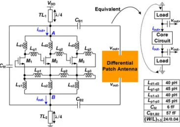
Fig. 1. Proposed triple-push oscillator with differential output.
Fig. 2. (a) Post-layout simulation result of differential output waveform. (b) Simulated input return loss and antenna gain of the differential patch antenna.
cated circuit topology is needed [3]. Power consumption and chip area are inevitably increased. Moreover, if passive balun is employed, induced passive loss degrades the available signal power.
In this letter, a triple-push oscillator with differential output is proposed by extracting output signals from the same current loop without requiring any additional balun or other circuits. Hence, the chip area can be small and the power consumption can be reduced.
II. DIFFERENTIALTRIPLE-PUSHOSCILLATORDESIGN
Fig. 1 shows the proposed triple-push oscillator that can pro-vide differential output. and are used for output impedance matching and dc blocking, respectively. used as RF chokes are realized by microstrip lines with electrical length of at the targeted frequency of 360 GHz. The os-cillator is essentially a ring osos-cillator topology. As the oscilla-tion condioscilla-tion is fulfilled, it oscillates and sustains stable signals
1531-1309 © 2014 IEEE. Personal use is permitted, but republication/redistribution requires IEEE permission. See http://www.ieee.org/publications_standards/publications/rights/index.html for more information.
864 IEEE MICROWAVE AND WIRELESS COMPONENTS LETTERS, VOL. 24, NO. 12, DECEMBER 2014
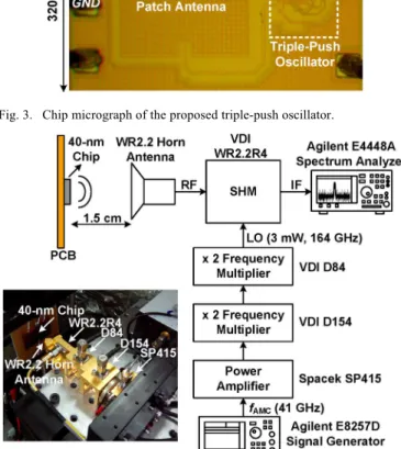
Fig. 3. Chip micrograph of the proposed triple-push oscillator.
Fig. 4. Experimental setup for measuring oscillation frequency and EIRP.
with equal amplitude but 120 phase difference at drain nodes of . By combining these signals through at node , the 3rd harmonics of these signals are added in phase while 1st and 2nd harmonics will be rejected. Hence, the oscillator can oscillate at , i.e., 3 , which is easily designed to be beyond . Note that is used to adjust the phase and ampli-tude of the fundamental signal at the drain and the gate to fulfill the optimal condition of transistors for power generation [2]. The same mechanism also applies at the source nodes of tran-sistors. By combining these signals through at node , another triple-push signal is obtained. Interestingly, the signals extracted from the source and drain nodes exactly have same amplitude but out of phase. The reason can be easily understood by an equivalent circuit shown in Fig. 1. Essentially, differential operation is guaranteed since differential output currents and are extracted from the same current loop. After con-verting to voltage domain by the Load, and shows perfect balanced form.
The oscillator is designed by observing activity condition of a transistor [2]. If , the oscillator can sus-tain stable oscillation. Transistor width is chosen as 1 for maximizing . With of 0.9 V, the transistor can pro-vide of around 250 GHz. Although bigger transistor size can give higher , inductors become not easy to be im-plemented since their inductance value will be too small for the frequency of interest. To have reasonable inductor size and maximize , the finger number of transistors is designed as 24. If these inductors are ideal, the oscillator can provide a
Fig. 5. Measured output IF spectrum.
Fig. 6. Measured EIRP and oscillation frequency versus supply voltage.
perfect differential output. However, in practice, a real inductor has parasitic capacitances that shunt the desired output currents, and , resulting in imbalanced outputs. To tackle this issue, is added to tune out parasitic capacitance at source nodes to avoid signal leakages from this parasitic path, which can improve output signal balance. They also make the layout more symmetric. Finally, the inductance value of and
, and and are designed as 45 pH and
40 pH, respectively, for oscillation at 360 GHz.
Transmission lines are used to realize the inductors. is di-rectly realized by a parallel plate using metal layers of M8 and M9 at the summing point located at the center of the layout. The layout arrangement is carefully planned to minimize coupling between the inductors. The whole chip, except the area around transistors, is simulated using ANSYS HFSS while intercon-nects between transistors to transmission lines are simulated by ANSYS Designer. The post-layout simulation indicates that the fundamental oscillation frequency is around 121 GHz. The simulated output voltage waveform is shown in Fig. 2(a). The amplitude and phase imbalance are only 0.7 dB and 2.4 , re-spectively. The output power can be as high as 11.1 dBm (100 load) at 363 GHz while only dissipating 31.5 mW from a 0.9 V supply. To assess the oscillator performance, the output differential signal is measured through antenna radiation of an on-chip differential patch with differential input impedance of 100 . The simulated frequency response of the differential patch antenna is shown in Fig. 2(b). The on-chip antenna can provide differential antenna gain of 7.8 dBi at 360 GHz.
III. EXPERIMENTALRESULT
The proposed oscillator is realized in 40 nm CMOS tech-nology. The chip micrograph is shown in Fig. 3. The chip size is , including dc pads. The oscillator core only occupies 0.028 . The chip is measured by an
LI et al.: 340 GHz TRIPLE-PUSH OSCILLATOR WITH DIFFERENTIAL OUTPUT IN 40 nm CMOS 865
TABLE I
PERFORMANCESUMMARY ANDCOMPARISONWITHPRIORWORKS
(a) Estimated by using simulated antenna gain of 10.5 dBi. (b) Active area. (c) Simulation result. (d) Whole transceiver area. (e) Measured using bolometer.
on-board setup. DC bias is given by wire-bonding to a PCB. The setup for measuring the oscillator frequency and output EIRP is illustrated in Fig. 4. The THz signal from the proposed triple-push oscillator transmits through air, received by a VDI WR2.2 diagonal horn antenna, and then down-converted by a VDI WR2.2R4 subharmonic mixer (SHM) to an IF signal. The IF spectrum can be measured by a spectrum analyzer. The required LO power of 3 mW for the SHM is generated by a chain of frequency multipliers and a signal generator generating a 41 GHz signal of 6.8 dBm. The chip is positioned around 1.5 cm from the horn antenna. The oscillator consumes only 34.1 mW from a 0.9 V supply, around 2.6 mW higher than the simulated result.
The measured output IF spectrum is shown in Fig. 5 as the supply voltage is 0.9 V. The measured IF frequency is 12.61 GHz. As the LO frequency increases by 1 GHz, the IF frequency decreases by 2 GHz. Hence, the oscillation frequency can be calculated by , i.e., 340.6 GHz, around 22.4 GHz lower than the simulated result. The measured IF power is 52.62 dBm after calibrating IF cable loss of 2.1 dB at 12 GHz. The EIRP of the proposed oscillator can be calibrated to be 21.8 dBm by using Friis transmission equation and noting that the conversion loss of the SHM is around 9.2 dB and the horn antenna gain is around 25 dBi at 340 GHz according to the datasheets provided by Virginia Diodes, Inc. The output power from the proposed oscillator can be estimated to be 11.3 dBm if the simulated patch antenna gain of 10.5 dBi at 340 GHz is used. The oscillation frequency and EIRP at different supply voltage are also measured and illustrated in Fig. 6. The measured result shows a similar trend with that of the simulated one. The EIRP can be increased up to 19.6 dBm as the supply voltage is 1.3 V. Table I summarizes the per-formance of the proposed triple-push oscillator and makes comparison with prior works [4]–[12]. Obviously, the proposed signal source can give differential output while consuming low dc power, providing high output power, and occupying small chip area.
IV. CONCLUSION
A low-power triple-push oscillator with differential output is proposed and successfully verified by experimental results. By
extracting and combining signals from source and drain nodes of transistors, the proposed oscillator can provide differential output without any other circuit required. Implemented in 40 nm CMOS, the measured result shows that the oscillator can oscil-late at 340.6 GHz while providing EIRP of 21.8 dBm. The power consumption is only 34.1 mW from a 0.9 V supply.
REFERENCES
[1] Y.-L. Tang and H. Wang, “Triple-push oscillator approach: Theory and experiments,” IEEE J. Solid-State Circuits, vol. 36, no. 10, pp. 1472–1479, Oct. 2001.
[2] O. Momeni and E. Afshari, “High power terahertz and millimeter-wave oscillator design: A systematic approach,” IEEE J. Solid-State Circuits, vol. 46, no. 3, pp. 583–597, Mar. 2011.
[3] J. Grzyb, Y. Zhao, and U. R. Pfeiffer, “A 288 GHz lens-integrated bal-anced triple-push source in a 65-nm CMOS technology,” IEEE J. Solid
State Circuits, vol. 48, no. 7, pp. 1751–1761, Jul. 2013.
[4] D. Shim, D. Koukis, D. J. Arenas, D. B. Tanner, and K. K. O, “553 GHz signal generation in CMOS using a quadruple-push oscillator,” in
Proc. VLSI Circuits Symp., Jun. 2011, pp. 154–155.
[5] E. Seok et al., “A 410 GHz CMOS push-push oscillator with an on-chip patch antenna,” in ISSCC Dig. Tech. Papers, Feb. 2008, pp. 472–629. [6] B. Khamaisi, S. Jameson, and E. Socher, “A 210–227 GHz transmitter with integrated on-chip antenna in 90 nm CMOS technology,” IEEE
Trans. Terahertz Sci. Technol., vol. 3, no. 2, pp. 141–150, Mar. 2013.
[7] J. Sharma and H. Krishnaswamy, “216- and 316 GHz 45-nm SOI CMOS signal sources based on a maximum-gain ring oscillator topology,” IEEE Trans. Microw. Theory Tech., vol. 61, no. 1, pp. 492–504, Jan. 2013.
[8] J.-D. Park, S. Kang, and A. M. Niknejad, “A 0.38 THz fully inte-grated transceiver utilizing quadrature push-push circuitry,” in Proc.
VLSI Circuits Symp., Jun. 2011, pp. 22–23.
[9] Y.-J. Chen and T.-S. Chu, “2-D direct-coupled standing-wave oscil-lator arrays,” IEEE Trans. Microw. Theory Tech., vol. 61, no. 12, pp. 4472–4482, Dec. 2013.
[10] V. Radisic et al., “Demonstration of a 311 GHz fundamental oscillator using InP HBT technology,” IEEE Trans. Microw. Theory Tech., vol. 55, no. 11, pp. 2329–2335, Nov. 2007.
[11] V. Radisic et al., “Demonstration of sub-millimeter wave fundamental oscillators using 35-nm InP HEMT technology,” IEEE Microw.
Wire-less Compon. Lett., vol. 17, no. 3, pp. 223–225, Mar. 2007.
[12] H. Eisele, “Third-harmonic power extraction from InP Gunn devices up to 455 GHz,” IEEE Microw. Wireless Compon. Lett., vol. 19, no. 6, pp. 416–418, Jun. 2009.