The
significant influence
of
surface states on the
electroluminescence
of
CdS
nanoparticles
Eih-Zhe
Lianga,
Ching-Fuh
Ljfl*a, Sheng-Ming Shih", Wei-Fang
Suba
GraduateInstitute
of
Electro-Optical Engineering
b
Institute
of
Materials Science and
Engineering
National
Taiwan University, Taipei
106,
Taiwan, ROC
ABSTRACT
The significance
of
surface statesin
nano-structuresis
studied using CdS nanoparticles. Spectral features like peakred-shift due
to
organic capping and influenceof
surface states have been observed. The pronounced enhancementof
emission from surface statescan be
dominant with certain modificationof
CdS nanoparticles. Spectral behaviorsof
electroluminescence
in
different temperatureare
also studied.Keywords: CdS nanoparticles, low-dimensional structure, surface states, electroluminescence, exciton.
1. ThTRODUCTION
Nanoparticles formed
by
chemical methods have certain advantages. They have low costof
production and wellcontrol physical properties. Compared with epitaxial quantum dots, nanoparticles can
be
simply dissolvedin
various solutions and appliedto
nonspecific substrates. Stimulated emission and optical gain had been reported with CdS quantum dotsby
optical pumping1'2. However,it
is
challengingto
employ electrical pumpingto
realize nanoparticle- based light emitting devices. Electroluminescence from CdS nanoparticles reportedin this
work provesthe
feasibilityof
using such materials
as
active light-emitting media.Since nanoparticles are low-dimensional materials
(
5
nm), compared with bulk materials,it
resultsin
large surface contact area with environment. Surface states formedby
termination with oxygenor
other contaminants are thusof
great amount. Generallythis
situationis
avoidedby
using passivation around nanoparticles,in
our case organicp-hydroxyl thiophenol group. However, we found that there can
be
significant enhancementof
light emission from surface states.It
can be
usefulin
additionto
intrinsic quantum states provided by low-dimensional structures.Electroluminescence
of
CdS nanoparticlesin
different environment suchas
normal treatment, heat treatment andoxygen enrichment
is
achieved. Emission spectrumof
CdS nanoparticlesis
significantly influenced by both process temperature and oxygen surrounding condition. Radiative recombination dueto
free excitonin
CdSis
observed, with spectral peak shift dueto
organic encapping. As surrounding oxygen content levelis
raised, radiative recombinationfrom surface states emerges. Side effect such
as
coalescenceof
CdS nanoparticle into bulk form also presentsin
raising process temperature.At
different temperature,the
EL spectrumof
CdS nanoparticle remains quitethe
same. Peak shiftis
compared with bulk bandgap shift and ascribedas
effectof
quantum confinement and surface configuration.This work also demonstrates
the
electroluminescenceof
CdS-nanoparticle on silicon substrate. The fabricationof
light emitting active layeris
simply the spin-coating technique. Carriersto
achieve light emissioncan
be
supplied by quantum tunneling through surrounding barrier into nanoparticles. Using silicon as substrate showsa
promisingway
tomonolithically integrate light emission
of
nanoparticles and conventional electrical circuitry. Moreover, optical functional blocks canbe
builtat
relatively low temperature, following traditional process. This advantage eliminates conflicted thermal budgetof
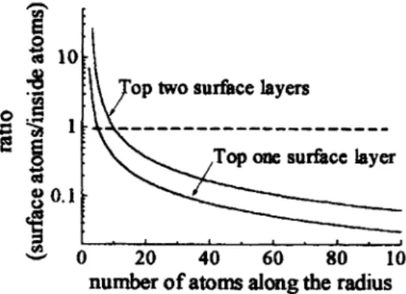
epitaxial 111-V materials and silicon circuitry.2. SIGNifICANCE
OF
SURFACE
STATESIn the
unpassivated case, nanoparticle interacts with oxygen as exposedto
atmosphere. Surface states associatedwith oxygen,
in our
case Cd-O bond,are
formed. The ratio between surfacearea
and volume ratioof
nanoparticle increasesas
individual particle size shrinks into several nanometer range. Radiative recombination rate with surface * Email:[email protected]; also with Graduate Instituteof
Electronics Engineering and Departmentof
Electrical Engineeringstates origin becomes comparable with that
of
CdS core,or
even dominant. Tobe
specific, assumingn
is the
numberof
atoms alongthe
radiusof
nanoparticle,the
ratioof
atomsin the
top surface layerto
core atomsis
given by(
n3- (n
-
m),)/
_ rn)3where
m is
effective numberof
atomsof
surrounding surface layer. We can seein
Fig. 1 thatthe
ratio becomes unity asthe
radius shrinks withinn
10.In
such cases, radiative recombination rateof
surface states becomes comparable tointrinsic ones, assuming alike oscillation strength. This situation describes how
the
unpassivated CdS nanoparticles can emit more light with surface state origin than that observedin
epitaxialor
bulk CdS case....-—' ..-— —.---—--
.
- . . !• . •_Fig. 1 Ratio
of
surface atomsto
core atoms with respect to numberof
atoms along radius.3.
PREPARATION
OF
MATERIALS
Two kinds
of
CdS nanoparticles ready for spin-coating purpose are synthesizedby
modificationof
Pietro'smethod3. First form
is
CdS nanoparticle with organic capping. Cadmium acetate dihydrate Cd(CH3COO)22H20, 0.80 g, 3 .0 mmole)is
dissolvedin
20 ml mixed solventof
acetonitrile, methanol, and water with volume ratio 1:
1 :2. Another solution containing disodium sulfide nanohydrate (Na2S9H20, 0.36g,
1.5 mmole) and p-hydroxyl thiophenol (0.56 g, 4.4 mmole)in
the
same solvent systemis
added into vigorously stirred cadmium acetate solution. The whole system was stirred for 18 hours without light illumination. After removing solvent and purifying by centrifuge, we obtained0.70
g
yellow solid aggregate ofCdS nanoparticles capped by p-hydroxyl thiophenol.Second form
of
CdS nanoparticleis
coated with silica shell. The purposeof
preventive useof
organic component isto
raisethe
thermal budgetof
whole fabrication processand
increase tolerance with low temperature. The preparation processis as
follows. Cadmium acetate dihydrate (Cd(CH3COO)22H20, 1.60 g, 6.0 mmole)is
dissolvedin
32 ml mixed solventof
acetonitrile and water with volume ratio 1:
1.
Another solution containing disodium sulfide (Na2SxH2O,x7—9, 0.58
g,
—2.4 mmole) and (y-mercaptopropyl) trimethoxysilane (1.41g,
7.2 mmole)in the
same solvent system is added into vigorously stirred solutionof
cadmium acetate. After being vigorously stirredfor
18 hours,the
mixture is basifiedto
pH=8.4 with 25% ofNH3 aqueous solution. Additional 64 mlof
ethanolis
addedto
the
mixture. The mixtureis stirred
for
48 hours after adding 1.89g
of
orthotetraethoxysilane (TEOS). Partof
the solvent was removed andprecipitation takes place
in
the mixture The precipitateis
centrifugedfor
three times and rmsed with deionized water2 n
E 0
.1o
'op two surface layers
I
,Top one surface layer
U 20 40 60 80 100
The prepared nanoparticle aggregate
is
redispersablein
ethanior
other polar organic solvents. After treated by ultrasonic vibration and percolation, solutions for spin-coating purposeare
produced.To
take
TEM image, prepared solution is dipped onto carbon film coated copper plate and reabsorbed. Sparselydistributed nanoparticles
are
obtained. The average diameterof
the spherical CdS nanoparticlesis
about 5 nm,as
shownin
Fig.2.
Compared withthe
high-temperature synthesizing methodby
using trioctylphosphine oxygen (TOPO), this room-temperature processis
easier butthe
particle size distributionis
wider.By
replacingpart
of
cadmium acetate with manganese acetate, we preparedMn
doped CdS nano- particles withdifferent concentrations
of
manganese (5%, 10% and 20%,in
molar percentage). Throughout the
experiment, no significant differenceof
doped and undoped CdS nanoparticlesis
found under the spectral resolutionof
ourmonochromator. To synthesize manganese doped CdS nanoparticles, we have used large molar percentage
of
Mn,5
%, 10% and 20
% respectivelyin the
reaction. However, only trace doping amountsof
Mn, 0.08%, 0.05% and 1 .10% wasdetected respectively
by
ICP-Mass investigations. Whenthe
same approach was usedto
synthesize MnS nanoparticles,a
very low yield was obtained. This indicates very low doping content canbe
made and electroluminescenceis
lessaffected
by
Mn content.4.
SETUP
FOR
ELECTROLUMINESCENCE
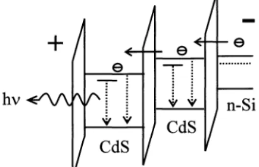
The basic idea about setup
of
electroluminescenceis to
use cascade tunneling as injection source. Carriers are suppliedby
tunneling current through potential barrierof
high bandgap material surrounding nanoparticle,as
shown in Fig. 3. In
our case,the
SiO groupor
organic functional group p-hydroxyl thiophenol servesas the
goal. The choiceof
substrateto
host CdS nanoparticlesis
silicon dueto
its
surface quality and availability.In
addition,in
this early studyof
light emission, difficultyto
maintain uniformityof
film existsif
nanoparticle solutionof
aqueous solvent system is used.The Schottky barrier
of
metal-silicon contact has certain prevention from short circuit other than indium-tin-oxide (ITO) glass.With different type
of
injection carriers, dependingon
n-typeor
p-type silicon substrate, electronsor
holes areemitted from silicon and holes
or
electrons are emitted from metal deposited. Fermi levelof
Siin
n-type case hasto
be raisedfor
electronsto
tunnel through potential barrierof
p-hydroxyl thiophenol group. Most carriers tunnel into theadjacent nanoparticles. Carriers are expected
to
recombine within nanoparticles through intrinsic radiative transition orsurface-state related transition.
Fig. 3 : Schematic ofelectron transport and transition in the device.
A
schematicof
CdS-nanoparticle light emitting stageis
shownin
Fig.4.
The fabrication stepsare as
follows. First,a
doped silicon wafer (dopinglO15
cm3)is
usedas
substrate. Acetone, methanol, andDI
water are used successively for clean procedure. Buffered oxide etchis
appliedto
remove native oxides. The waferis
spin-coated with CdS nanoparticle solutions. Solvents are either removedby
evacuationor
heat treatment. The thicknessof
CdS nanoparticle layer canbe as
largeas
500 nm, verifiedby
surface profile scan.In
this case, volume density canbe
very high.Subsequently, both top and bottom metal contacts
are
madeby
thermal evaporation. The top semi-transparent contact layer is lOnm gold, andthe
bottomis
l5Onm gold. Beforethe
depositionof
the Au
layer,a
3-nm adhesion layerof
chromiumhad
been evaporated for both contacts.A
CM1 10 monochromator and photomultiplieris
usedto
record theelectroluminescence spectrum. In every spectrum measurement, the entrance
slit
width 0.6 mmis
used for maximum detectionand
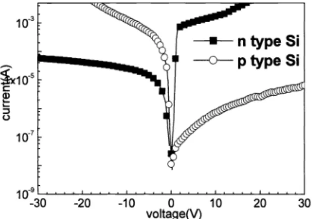
correct spectrum.Samples made
on n- and
p-type Si wafers show different current-voltage curves,as
shownin
Fig.5.
Both haverectifying current-voltage (I-V) curves,
but
with opposite polarities. This rectifying effect corresponds to metal-insulator-semiconductor tunneling effect as expected. Tobe
specific,the
thin potential barrierof
organicfunctional group and low substrate doping level results
in
Schottky-diode-like behavior.Fig. 5: I-V curves ofdevices on n-type and p-type Si.
5.
PROPERTIESOF
ELECTROLUMINESCENCE
We take different post treatments after the nanoparticle film
is
spin-coated onto silicon substrate. The normal treatmentis
to
removethe
solvent without physical changeof
nanoparticles. Heat treatmentis
carriedout in
mediumhigh temperature
to
explore decomposabilityof
organic passivation andtest
oxygen cooperation. Oxygen enrichmentraises extent
of
oxygen related surface states. All three conditions show prominent spectral features andcan be
usedto
monitor passivationof
surface condition.Origins
of
electroluminescenceof
CdS nanoparticle with bulk CdS are schematically shownin
Fig. 6. Threeexciton levels corresponding
to
bulk CdS bandgap now change their peak positionsof
quantum states due to modificationof
surface configuration. Modified A free exciton level changes from 508nmto
526.5nm ascan
be determinedin
normal treatmentof
electroluminescence device. Transition levelof
surface states relatedto
Cd-Otermination with peak position
of
571 .Snm canbe
observed. This level occurs when passivationof
nanoparticle is removed andit
has contact with atmosphere,as
in
heat
treatment and oxygen enrichment.with
cappingE
526.5nni 571 .5nm 508nm ______E
A' Excitonn levelFig.
6
Energy diagramof
CdS nanoparticle.Fig. 4: Schematic
of
the CdS nanoparticles EL device on Si wafer.voltage(V) Bulk CdS
E
_________ 'I, EVA XEB
EB
EC
EC
'Jr Surface states3.1 Normal process
After spin-coated,
the
deviceis
placedin
a
chamber with evacuation at room temperature for5
minutesto
removeethanol solvents. Both spectra
of
CdS and CdS doped with Mnare the
same,as
shownin
Fig.7.
The spectrum fits into Lorentzian shape with scattering timeof
6
fs. Its FWIIMis 42
nm. Such broad spectrum indicatesthe
dispersionof
particle size anda
trade-offof
low temperature synthesis.This spectral peak indicates radiative recombination
of
free excitonin
CdS nanoparticles with red-shift dueto
p-hydroxyl thiophenol groups. The green spectral peakis
at 526.5nm (2.355eV), different from bulk CdS A-excitontransition energy, 2.441eV (508nm) at room temperature. Although quantum confinement within
the
nanoparticles increases exciton energy wheneverthe
particle size decreases4'5, organic functional groupor
silicon dioxide matrix canmodify
the
electron configuration within and change ground states significantly.It
resultsin
energy red-shiftof
86 meV. CdS nanoparticles coated with poly(vinyl alcohol) also show such energy shiftin
absorption spectrum6, where photoluminescence at 2.42eV (10K)is
observed.Fig. 7: EL Spectrum
of
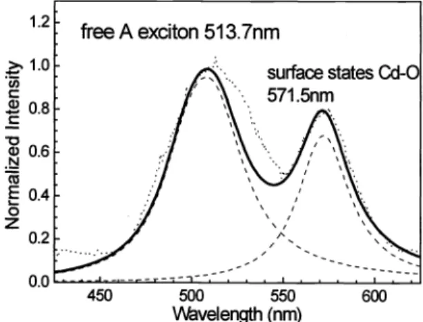
CdS with solvent removed. 3.2.Heat
treatmentThe CdS nanoparticles
are
spin-coatedas
describedin
previous section. These samplesare
subsequently treatedby
rapid thermal annealing (RTA) with temperature 425°C for5
minutes. The annealing process takes placein
nitrogenpurge and its purpose
is to
remove solvent and bothtest
decompositionof
organic functional group. Electrical propertylike I-V curve resembles that
in
Sec. 3.1.As
shownin
Fig.8 the
emission spectrum consistsof
two peaks. Oneis
at513 .7nm and
the
other at 571.Snm. The former peak standsfor
bulk CdS freeA
exciton transition. This spectral lobe canbe
fittedby
Lorentzian shape with scattering timeof
8
fs and FWHM 40 nm.1.2 1.0
>
Cl) C.
C 0.8 ci) N a) E 0z
0.6 0.4 0.2 450 500 550 \veIength (nm) 600Fig. 8: The EL Spectrum of CdS particles after heat treatment.
500 550
wavelength (nm)
The 57 1 .5nm peak results from
the
trapped carriersin
surface states relatedto
oxygen, Cd-O termination7. Inmedium high temperature treatment, decomposition
of
p-hydroxyl thiophenol group causes oxygen termination withcadmium
to
occur.It
proves p-hydroxyl thiophenol groupto be
effective overcoatof
CdS nanoparticles against oxygeninfluence. The surface states induce radiative transition
as
well. The peak magnitude atthe
spectral lobeis
smaller thanthe magnitude
at
5
13.7
nm, indicating emission from surface statesis
weaker than that resulted from CdS nanoparticles.However, light power from this sample
is
generally stronger than thatin
Sec.3 .
1.
This phenomenonis
dueto
theparticipation
of
surface level luminescence, leadingto
increaseof
total light output.3.3 Effect
of
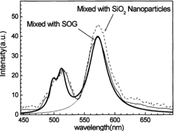
surrounding oxidesTo further study the surface states related
to
oxygen, we immersed CdS nanoparticles into high oxygen content environment. Two waysare
proceeded. First,the
nanoparticle solutions were mixed with spin-on-glass (50G Filmtronics3
15FX), and the second way, mixed with 5102 nanoparticles (average diameterof
12 nm, dissolved in isopropanol). The cleaned, oxide-free silicon substrateis
spin-coated and treatedby
425°Cto
sinter with 5i02 glass. Thesimilar EL spectrum
is
foundin
mixtureof
CdS nanoparticles with SOG and 5i02 nanoparticles. The peakat
513.7nm (2.414eV) resemblesA
free exciton signalof
bulk CdS at temperature 65°C, andthe
peakat
57l.5nm (2.414eV) correspondsto
radiative transition dueto
surface states. The magnitudeof
total light emissionin
current setupsis
tentimes stronger than that
of
unheated samplesin
Section3 .
1,
under the same carrier inj ection condition.Co Cl)
ci
Fig. 9: EL spectrum ofCdS nanoparticles with oxygen enrichment
EL
spectrum shownin
Fig.9 indicates two mechanismsas
shownby the
energy diagramin
Fig.6.
First, thecoalescence
of
CdS nanoparticles into bulk form resultsin
less broadening spectrum around5
13 .7 nm. Since thepotential barrier
of
p-hydroxyl thiophenol group disappears dueto
decomposition, carriersin
bulk powders stay forenough time (about
ins
transition lifetime)to
recombine radiatively between each tunneling process. Second, relativemagnitude
of
surface states luminescenceis
much stronger than thatin
Sec. 3.2. Highly increased concentrationof
surface state levels, which are suppliedby
surrounding oxygen termination, contributesto
the enhancementof
internalquantum efficiency. The magnitude difference between mixture with SOG
and
Si02 nanoparticles comes from excessdangling Si-O bond
of
the
latter case. With the same sintering time,the
latter mixture makes more extentof
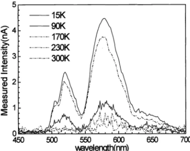
oxygen enrichment.3.4 Temperature effect
To examine EL property
of
CdS nanoparticle with varied temperature, original organic functional group issubstituted with inorganic silica passivation shell,
in
orderto
prevent instabilityof
organic composition at low temperature.EL
spectraof
silica-passivated CdS nanoparticles are shownin
Fig. 10. The resembling peakof
surfacestates represents Cd-O termination, now introduced
by
silica passivationat
surrounding surface probesto
originof
light emission.As
temperature increases, theEL
intensity decreases. Such reduced emission efficiency comes from increasednonradiative mechanism with increased temperature. Surface states
and
carrier-phonon scattering both play roles. Tentimes stronger magnitude
of
light emission intensityat
low temperatureof
15K
compared with room temperature case reveals that nonradiative mechanismis
a
crucial factor influencing emission efficiencyof
the emitter. The reasonfor
thesimilar spectra is due
to
two causes. First, the shiftof
quantized energy levels dueto
small nanoparticles (<5nm)contributes
to the
spectrum around 520nm. Second, transitionof
surface states may have multiple levels correspondingto
broad spectrum at room temperature.C >s C,) cD U) Co ci 700
Fig. 10: EL spectrum
of
CdS nanoparticles with silica shell at varied temperature.Spectral peak at 520nm
in
Fig. 10is
attributedto the
same originas
peakat
526.5nmin
organic-capped CdS nanoparticles, with additional effectof
quantum confinement and surface configuration.As
a
result, peak shift withvaried temperature
is
compared with bulk bandgap shiftin
Fig. 11 and ascribedas
characteristicsof
as-synthesized CdSnanoparticle. Ten times increase
of
emission intensityis
observedat
cryogenic temperature (15K), indicating stronginfluence
of
surface traps dueto
the
large surface area. Reduced thermal scattering also contributesto
enhancementof
light emissionat
low temperature. The relative magnitudeof
recombination rateof
surface statesto
exciton levelchanges slightly and may result from
its
nearnessto
conduction band2.5
2.4
0 100 200 300
Terrperature (K
Fig. 11: Spectral peak variation with temperature compared with bulk exciton energy.
With energy parameters
of
bulk CdS given above6, red-shift dueto
p-hydroxyl thiophenol groupis
determined as 86meV. Also, transition levelof
surface statesis
foundto be
273 meV below bulk bandgap.In
additionto
observationof
such peakat
571 .Snm, similar phenomenaat
spectral range, SSOnm—600nm, asan
indicationof
imperfect CdS crystalor
nanoparticleshad
been reported elsewhere. Okamoto8 also ascribedtheir
broad peakat
6SOnm (1 .9eV)to
surfacestate emission. Hong7 also demonstrated broad peak
of
592nm (2.0944eV) dueto
S-vacancy(in
this case terminationof
oxygen).3.5
Raman
spectrumPreviously observed transition
of
manganese ionin
CdS nanoparticle at S8Snm (2. 1 19eV)9is not
clearly observedin
our samples, mainly dueto
insufficient spectral resolution and trace contentof
Mn
incorporatedto
CdS core. To550 600
v.eveIength(nm)
•
Free Aexaton (exp.)•
Free A exaton incaJ4
determine
the
factoron
firm ground, Raman spectroscopyis
taken as shownin
Fig. 12.Raman shift
at
305cm1 correspondsto
the
longitudinal optical phonons LO) modeof
bulk CdS'°.No
wave number shiftis
observedfor
CdSIMn nanoparticles, therefore Mnis not in the
CdS core lattice. The other Raman shiftpeaks
are
fromthe
vibrationsof
the organic molecules. Consequently,the
EL peaksof
CdS nanoparticles prepared withor
without additionofMn
arethe
sameas
shownin
Figure 7.We have mentioned reaction rate
of
MnS synthesisis
slower than thatof
CdS synthesis. Therefore, theposition
of
Cdin the
latticeof
CdS can barelybe
replaced by Mn.It
is
trappedby the
hydroxyl groupof
p-hydroxyl thiophenol capping onthe
surfaceof
CdS nanoparticles.5. CONCLUSIONS
Significant surface influence
is
observed for nanoparticles. Chemical preparationof
CdS nanoparticles ready forspin-coating and LEDs made
of
CdS and CdS:Mn nanoparticles on Si substratesare
describedin
detail.EL
propertiesare
investigated. Spectral shiftof
free exciton transition dueto
passivationof
p-hydroxyl thiophenol group around nanoparticlesis
discovered. Process modifications suchas
heat treatment and oxygen enrichmentare
influentialto
intrinsic green emission. P-hydroxyl thiophenol groupis
shownto
have protection from diffusionof
contaminants into nanoparticles,but
cannot resist temperature deterioration above 400°C.Radiative recombination
of
carriers trappedin
surface states present and magnifiesitself as
long as extentof
surface states increases. Ten times increaseof
emission intensityis
observedat
cryogenic temperature (1 5K), indicatingstrong influence
of
surface traps dueto the
large surface area. Reduced thermal scattering also contributes toenhancement
of
light emissionat
low temperature.At
varied temperature,the EL
spectrumof
CdS nanoparticle remainsquite
the
same. Peak shiftis
compared with bulk bandgap shift and ascribed as effectof
quantum confinement and surface configuration.ACKNOWLEDGEMENTS
The authors acknowledge
the
support from National Science Council, ROC underthe
contract number NSC 90-2215-E-002 and NSC 90-2622-L002.REFERENCES
1. V.1. Klimov, A.A. Milkhailovsky, Su Xu, A. Malko, J.A. Hollingsworth, C.A. Leatherdale, H.-J. Eisler,
and
M.G. Bawendi, "Optical Gainand
Stimulated Emissionin
Nanocrystal Quantum Dots,"
Science 290, pp.3 14-3 17, 2000.2.
J.
Butty, Y.Z. Hu, N. Peyghambarian, Y.H. Kao, and J.D.Mackenzie, "Quasicontinuous gainin
sol-gel derived CdSquantum dots
,"
App!. Phys. Lett. 67, pp.2672-2674, 1995.3 .
J. G. C. Veinot,M.
Ginzburg, and W.J.
Pietro, "Surface Functionalizationof
Cadmium Sulfide Quantum-Confined Nanoclusters.3.
Formation and Derivativesof
a
Surface Phenolic Quantum Dot ,"Chem. Mater.9,
pp.2117-2122, 1997.4.
B.G. Potter, Jr. and J.H. Simmons, "Quantum size effectsin
optical propertiesof
CdS-glass composites," Phys. Rev. B6661
'6-I
dd
'Z9Z1
'SJOOflpUOO!WOS OU!jjt2Si(IOOUU SpDJO 1doosoipods uuw>j,,'ioqo
MSpu
qo
cs
'nqs
NS
'us
MS'puN
rioi
sc
T
UON•i4j
sp!1os1'gjq,jq
'99-Lc9dd661
Jo sUJodoJd
pu
sisoquX
ssooid
p-jos
U! SJSfljO Jo2onpuoolluos,, Hpui
'oid.iyj
'joqudS
T
6 866T '1I-Ldd 'SOT UflWWOJ 31flJp//Og UOIW!OXO OAUOIOS Xq sj sj(jzouguSp
s
'1piu1A
oouoosouiwnjooq,,wag
poddio-ooijnspui 'iqso)pJnJAJ
,j
'1M1)joso]j H'nswu,I
A'o3owjO
s
8 000Z '9Z-6Udd '81Z tI10JD71'3
T
'pOqw
uoU1Wjqns/q
UMOJspjj°
soiodoidjiodo
'uiqg TAU1
'UOOAf3
'UOOf 'UOH I TX L OOO 't'117-OWdd 'SIz/Iz'1°D
l"'J
'1)jUJ
1 '!OA
'OOWflS1JAI soiiodoid podopunjopui
podopuys4pj
sps(ioouiu
U!'wXjod
T
TAT 9 1661 'ZZE8-6O8dd 'S6