Hot carrier recombination model of visible electroluminescence
from metal–oxide–silicon tunneling diodes
C. W. Liu,a)S. T. Chang, W. T. Liu, Miin-Jang Chen,b)and Ching-Fuh Linb) Department of Electrical Engineering, National Taiwan University, Taipei, Taiwan 共Received 26 June 2000; accepted for publication 16 October 2000兲
We report the visible electroluminescence at room temperature from metal–oxide–silicon tunneling diodes. As biased in the Fowler–Nordheim regime, the electrons tunnel from the gate electrode through the ultrathin oxide and reach the Si anode with sufficiently high energy. The hot electrons cause the impact ionization, and generate the secondary hot electrons and hot holes in Si substrates. The visible light comes from the radiative recombination between the secondary hot electrons and hot holes, and the hot carrier recombination model can fit the visible electroluminescence spectra. © 2000 American Institute of Physics.关S0003-6951共00兲02751-0兴
Continuous attempts have been made to realize viable light sources on Si, and the integration of light emitters and detectors in the metal–oxide–silicon共MOS兲 compatible pro-cess makes the optical interconnects feasible for ultralarge scale integration circuits.1,2 The study in the past was fo-cused on the structure of p – n junctions. Two different Si light emitters have been reported using p – n diodes. A narrow-band infrared emitter at 1160 nm was implemented using a p – n junction under forward bias.3 A broadband 共450–850 nm兲 visible-light emitter was also realized using an avalanche p – n diode.3,4This visible light emission from the avalanche bias of p – n diodes has been explained by a Bremsstrahlung model,5an intraconduction band recombina-tion model,6and a hot electron recombination model.7
Recently, MOS tunneling light emitting diodes have also shown the infrared band edge electroluminescence 共EL兲8 at accumulation bias. There are also reports on visible EL from MOS structures, and the origin has been attributed to oxide defects9and hot electrons.10In this letter, we report that a hot carrier recombination due to the impact ionization of the tunneling hot electron is responsible for the visible emission and the line shape of the visible emission can be fitted by this model.
The ultrathin gate oxide of the MOS tunneling diode used in this study is grown by rapid thermal oxidation共RTO兲 at 900 °C. The gas flows are 500 sccm nitrogen and 500 sccm oxygen at the pressure of 250 mbar. Before oxidation, the sample was cleaned by a HF dip. An in situ hydrogen bake at 900 °C for 2 min was performed before the growth of the RTO. The temperature was measured by a pyrometer with a close loop control. Although the interface state den-sity of Si/oxide interface cannot be accurately measured by the capacitance–voltage method due to the gate leakage cur-rent, the measurement on dark current of the similar devices11and on thick oxide samples indicates that the inter-face state density is within 1⫻1011cm⫺2. The nominal thickness of the oxide is about 3 nm, measured by ellipsom-etry. The resistivity of the 100 mm p-type 共100兲 wafers is
1–10⍀ cm. The N 共n-type兲 MOS diodes have an indium tin oxide 共ITO兲 gate electrode with circular areas of 4 ⫻10⫺2cm2 defined by photolithography. The visible light can pass the transparent ITO gate electrode and the detection signal can be increased. Note that for nontransparent elec-trode, a special structure is needed to observe the visible light from the edge of the MOS diodes with poly Si electrodes.10
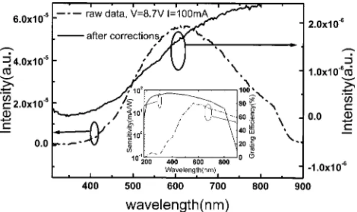
For the ITO gate under negative bias, the electron in the ITO tunnels to the Si substrate through the thin oxide. The negative gate bias also attracts the hole at the Si/SiO2 inter-face to form an accumulation region. At sufficiently large negative gate bias共⬎6 V兲, visible light is observed as shown in Fig. 1. Since visible EL has a very broad spectrum, cor-rections due to the sensitivity of photomultiplier tube共PMT兲 and the grating efficiency have to be taken into account. Figure 1 shows both the raw data obtained directly from the photomultiplier tube and the processed data after such cor-rections. The inset of Fig. 1 is the detector sensitivity and grating efficiency used for such corrections. The cutoff of the PMT is around 800 nm共1.55 eV兲. The raw data show a peak around 600 nm, but the processed data do not. This indicates the necessity of such corrections.
Figure 2 shows the visible spectra after corrections at different bias. The emission intensity increases with increas-ing bias voltage. The radiative recombination between tun-neling electrons and accumulated holes seems unlikely
re-a兲Also at Graduate Institute of Electronic Engineering; electronic mail: [email protected]
b兲Also at: Institute of Electro-Optical Engineering.
FIG. 1. The visible emission spectrum before and after corrections from MOS tunneling diodes. The inset is the detector sensitivity and grating ef-ficiency used for corrections
APPLIED PHYSICS LETTERS VOLUME 77, NUMBER 26 25 DECEMBER 2000
4347
sponsible to the visible emission, since the spectra does not change significantly in shape as the negative gate bias in-creases from the 5.9 to 8.7 V.10 The energy of tunneling electrons reaching Si increases with the increasing gate volt-age. The high-energy portion of the spectra would be more and more significant as the negative gate bias increases if the tunneling hot electrons recombined directly with holes. As reaching the Si, the tunneling electron has sufficient energy to cause the impact ionization at high negative gate voltage. The secondary hot electrons and holes are produced by the impact ionization共Fig. 3兲. The hot electron distribution func-tion due to the impact ionizafunc-tion has been derived by Wolff12 and is given by
f共E兲⬀exp共⫺E兲关1⫺Ei共E兲/Ei共E0兲兴,
where Ei(x)⫽兰⫺⬁x 关exp()/兴d, ⫽1/kBTe, Te is the tem-perature, and E0 is the ionization threshold to generate the secondary electrons and holes. The Wolff’s distribution sub-stantially below the ionization threshold is quasi-Maxwellian, and the electron temperature can be much higher than the lattice temperature.12Two different values of the impact ionization threshold of electrons were used in the
literature. One is one and half of Si band gap,7,13 the other one is 3.6 eV.14For the photon energy interested共1.5–3 eV兲, the Wolff’s distribution is very close to quasi-Maxwellian if the 3.6 eV is used for ionization threshold. Due to the large density of states and large ionization threshold of holes共5.0 eV兲,14the hot hole distribution function is commonly repre-sented as quasi-Maxwellian.7,13 Similar to the electron-hole plasma recombination model,8 the momentum conservation in the indirect band gap Si is assumed to be conserved by impurity scattering, roughness scattering, and other mechanisms.8 The emission line shape is a simple convolu-tion between electron and hole populaconvolu-tions. Since the signal of the PMT detector is photon energy, not photon count, a photon energy weighting factor (h) is also included in the hot carrier recombination model, which is
I共h兲⫽I0
冕
0h⫺Eg
hDe共E兲Dh共h⫺Eg⫺E兲
⫻ fe共E,Te兲fh共h⫺Eg⫺E,Th兲dE,
where De and Dh are the densities of states of electron and
hole, respectively, h is the energy of photon emitted, Eg is
the Si band gap, Teand Thare the hot electron and hot hole temperatures, respectively, the electron distribution function
fe is Wolff’s, and hole distribution function fh is quasi-Maxwellian. Figure 2 shows the theoretical curves of the emission line shape, which give the reasonable fit of experi-mental data. The theoretical line shape drops more slowly if the electron distribution function is quasi-Maxwellian as compared to the Wolff’s distribution with E0⫽1.5 eV. Note that the theoretical curves using quasi-Maxwellian electron distribution are overlapped with those using Wolff’s distri-bution with E0⫽3.6 eV in Fig. 2. For simplicity, we used the same Te and Th in the fitting. The carrier temperature
in-creases from 2845 to 3075 K as the bias inin-creases from 5.9 to 8.7 V. This indicates that the higher energy of tunneling electrons can produce secondary hot carriers with higher en-ergy, and thus leads to higher carrier temperature. The ion-ization threshold of 1.5 eV gives a better fit than 3.6 eV in Fig. 2. For PMOS diodes共n-type substrate兲, no visible light was detected. This is probably due to the much lower impact ionization rate of holes14in Si, as compared to electrons. The tunneling hole from the gate electrodes into Si substrates cannot produce sufficient hot electron and hot hole popula-tions, and therefore, the visible light is too weak to be de-tected.
A visible light is observed from MOS tunneling diodes with ITO gates. The similar emission spectra have been ob-served in p – n junction under an avalanche bias. The origin of the emission in p – n junctions has been attributed to dif-ferent mechanisms such as the Bremsstrahlung effect, the intraconduction recombination, and the hot carrier recombi-nation and is still under debate. We, however, demonstrate that the visible emission in MOS structures is due to the hot carrier recombination, which are generated by high-energy electron tunneling from electrodes to p-type Si as biased in the Fowler–Nordheim regime. The theoretical line shape fits the experimental data reasonably well.
This work is supported by National Science Council, Taiwan, Republic of China共002-017, 89-2218-E-FIG. 2. The measured visible spectra from MOS tunneling diodes with ITO
gates and the theoretical line shape from the hot carrier recombination model. Note that the theoretical curves using quasi-Maxwellian distribution are overlapped with those using Wolff’s distribution with E0⫽3.6 eV.
FIG. 3. The schematic diagram of the hot carrier recombination model.
002-012, 89-2112-M-002-034, and 89-2215-E-002-016兲. The support from the Yen Tjing Ling Foundation is also highly appreciated.
1
K. Misiakos, E. Tsoi, E. Halmagean, and S. Kakabakos, Tech. Dig. Int. Electron Devices Meet. 25共1998兲.
2C. W. Liu, M. H. Lee, C. F. Lin, I. C. Lin, W. T. Liu, and H. H. Lin, Tech. Dig. Int. Electron Devices Meet. 749共1999兲.
3
J. Kramer, P. Seitz, E. F. Steigmeier, H. Auderset, and B. Delley, Sens. Actuators A 37–38, 527共1993兲.
4L. W. Snyman, M. du Plessis, E. Seevinck, and H. Aharoni, IEEE Elec-tron Device Lett. 20, 614共1999兲.
5
T. Figielsky and A. Torun, Proceedings of the International Conference on the Physics of Semiconductors, Exeter, UK, 1962, p. 853.
6J. Bude, N. Nano, and A. Yoshii, Phys. Rev. B 45, 5848共1992兲. 7A. T. Obeidat, Z. Kalayjian, A. G. Andreou, and J. B. Khurgin, Appl.
Phys. Lett. 70, 470共1997兲.
8C. W. Liu, M. H. Lee, M.-J. Chen, I. C. Lin, and C.-F. Lin, Appl. Phys. Lett. 76, 1516共2000兲.
9J. Yuan and D. Haneman, J. Appl. Phys. 86, 2358共1999兲.
10R. Versari, A. Pieracci, M. Manfredi, G. Soncini, P. Bellutti, and B. Ricco, Tech. Dig. Int. Electron Devices Meet. 745共1999兲.
11C. W. Liu, W. T. Liu, M. H. Lee, W. S. Kuo, and B. C. Hsu, IEEE Electron Device Lett. 21, 307共2000兲.
12P. A. Wolff, J. Phys. Chem. Solids 16, 184共1960兲.
13S. Yamada and M. Kitao, Jpn. J. Appl. Phys., Part 1 32, 4555共1993兲. 14S. Sze, Physics of Semiconductor Devices共Wiley, New York, 1981兲, pp.
45–47.
4349