國 立 交 通 大 學
光電工程研究所
碩 士 論 文
高壓水處理技術應用於鍺型金氧半
元件之研究
Study of High Pressure Water Treatment for
Germanium-based MOS Device
研 究 生 : 吳 明 聰
指導教授 : 劉 柏 村 博士
中 華 民 國 一百 年 八 月
高壓水處理技術應用於鍺型金氧半元件之研究
Study of High Pressure Water for Germanium-based MOS
Device
研 究 生:吳 明 聰 Student:Ming-Tsung Wu
指導教授:劉 柏 村 博士 Advisor:Dr. Po-Tsun Liu
國 立 交 通 大 學
光 電 工 程 研 究 所
碩 士 論 文
A Thesis
Submitted to Department of Photonics Institute of Electro-Optical Engineering College of Electrical and computer Engineering
National Chiao Tung University In partial Fulfillment of the Requirements
the Degree of Master In Electro-Optical Engineering August 2011
中 華 民 國 一百 年 八 月
i
高壓水處理技術應用於鍺型金氧半
元件之研究
研究生:吳 明 聰 指導教授:劉 柏 村 博士
國 立 交 通 大 學
光電工程研究所
摘要
鍺半導體由於擁有較高的電洞和電子遷移率,被視為是下一世代奈米電子元件 技術中最有希望取代矽而成為電晶體主動層的半導體材料,但是次氧化鍺(GeOx)的 熱穩定性較差,使得元件製作過程中的高溫製程將會劣化Ge-MOSFET 的元件特性。 因此,為了消除次氧化鍺熱解造成的元件劣化情形,我們提出了高壓水處理的技術 (低溫的超臨界流體),以消除次氧化鍺熱層穩定為主要目的。所以我們研究了鍺型 金氧半元件在超臨界二氧化碳流體混合水的處理下其電性的改變以及其機制探討。 首先,我們對在鍺基板上剛濺鍍完的二氧化鋯使用250o C真空爐管退火並且做為基準 片,而後再分別對其進行300o C、400o C、500o C通氮氣快速退火30秒,來研究其因熱 所造成的元件劣化情形,接著再挑選500o C退火的試片對其進行溫度為100°C壓力為 3000psi的二氧化碳超臨界流體混合水處理持續一小時;後續我們使用了高解析穿透 式電子顯微鏡以及X光光電子能譜儀,驗證超臨界流體混合水能有效的使水分子擴 散至二氧化鋯到達鍺通道和二氧化鋯的界面,進而再介面中產生氧化還原反應,其 中包含氧化為完全鍵結的鋯元素以及還原次氧化鍺回鍺元素,使次氧化鍺層能夠消 除,且整體的閘極氧化層厚度下降,也修補了因次氧化鍺熱解造成的元件劣化情形, 降低閘極漏電流;對經過退火後的元件作超臨界處理,發現元件特性得到改善,顯 示出超臨界二氧化碳流體混合水的確具有通過閘極氧化層進而擴散到鍺通道表面去 做還原氧化的能力。除此之外,我們利用常壓的水氣快速退火來驗證是否水的處理 能夠產生次氧化鍺的還原反應,由結果顯示,不論是高壓還是常壓的水處理都具有 在二氧化鋯以及鍺通到界面產生氧化還原的能力,使得次氧化鍺能夠消除,不過高 壓水處理的方式對於消除次氧化鍺的能力確實比常壓水處理的方式來得較具效果; 通過適當的退火溫度也可以對界面產生修補的作用,所以低溫超臨界流體混合水的 技術,能減少次氧化鍺層的厚度,並且改善鍺型元件的特性。可預期的,若將超臨 界流體的特殊特性整合在鍺型電晶體元件的製作上,去修補因為後續高溫製程對元 件產生的劣化情形,對於未來高效能鍺型MOSEFT發展,將具有其優勢以及前瞻性。ii
Study of High Pressure Water Treatment for
Germanium-based MOS Device
Student:Ming-Tsung Wu Advisor:Dr. Po-Tsun Liu
Department of Photonics Institute of Electro-Optical Engineering
National Chiao Tung University
Abstract
Germanium (Ge) semiconductor has been considered as an alternative channel material in replace of Si for future high-performance CMOS technology, because its higher carrier mobility for both electrons (2.6 times) and holes (4.2 times). However, the Ge-MOS technology has the most critical issue hindering the application of Ge is lack of high-quality and stable Ge sub-oxide (GeOx). In this study, to solve the
thermal decomposition of GeOx the high pressure water treatment (supercritical fluids
technology) is employed originally to eliminate the GeOx interlayer and improve the
properties of ZrO2 high-k film. First, the thermal stability of ZrO2/Ge stack is
analyzed by the sample treated with 250oC high vacuum furnace annealing for 30min and then treated by 300oC, 400oC and 500oC N2 RTA for 30s respectively. Second, the
high pressure water treatment (SCF) at 100oC and 3000psi for 1hr used to the sample which is treated by 500oC N2 RTA for 30s. By HR-TEM, XPS analyses, it can verify
iii
the elimination of GeOx interlayer due to the SCF treatment surely, and it can explain
the improvement of the gate leakage after SCF treatment. According to the many reference paper, we indicate the mechanism about the reduction of GeOx interlayer in
ZrO2/Ge by SCF treatment. Besides, the Water Vapor Annealing is used to verify the
water treatment has the ability of redox in the ZrO2/Ge stack, and though the
annealing by suitable temperature can repair the interface to improve the electric characteristic of ZrO2/Ge device. The SCF treatment on high performance
iv
誌 謝
首先我要先感謝我的指導教授:劉柏村教授,提供完好的研究環
境以及豐富的資源,並且在實驗上給予我寶貴的意見讓我受益良多。
除了有完善的設備、高水準的師資與研究團隊可以隨時與世界頂尖研
究成果爭雄,實驗室注重文能力培養也讓我不忘踏出自己關門的研究,
培養國際化的能力與視野,成為全方位的人才,未來可以為校爭光回
饋社會。
在這兩年來研究的旅途上,我最感謝指導我的學長黃震鑠學長,
常常不厭其煩的教導我如何研究、如何安排與規劃實驗,也教導我許
許多多在學術上我遇到挫折該如何去面對,真的是由衷的感激;再來
感謝其他實驗室的學長,鄒一德、鄧立峯和竹立煒學長,時時不斷的
給我關心以及共度生活上的一些瑣事;也感謝陪伴我的實驗室的同學
楊孟娟與范揚順,一起研究一起休閒,有了他們讓實驗生活更加多采
多姿;此外,還要感謝學弟妹們,不論是在實驗上還是實驗室生活的
陪伴,有你們真好。
最後,也是最重要的,要感謝我的父母吳塗情先生以及黃玉清小
姐,感謝他們的養育之恩,常常在我最困頓的時候給予我莫大的鼓勵
與支持,千言萬語都說不來我對父母的愛與感謝;另外,特別要感恩
我生命中的導師,您給予我的,我只能用全力以赴的心,以報師恩;
感謝大家的支持與陪伴,讓我可以順利的邁向人生的下一階段,感謝
有你們。
吳明聰 2011 年 8 月
v
Contents
Chinese Abstract --- i
English Abstract --- iii
Chinese Acknowledgment --- v
Contents --- vi
Table Captions --- ix
Figure Captions --- x
Chapter 1 Introduction
1.1 General Background --- 1 1.2 Motivation --- 4 1.3 Organization of Thesis --- 6Chapter 2 Experiment Instrument and Process
2.1 Experiment Instruments --- 102.1.1 RF - Sputter --- 10
2.1.2 Water Vapor Rapid Thermal Annealing System --- 12
vi
2.2 Process Flow of Zirconium Oxide on Germanium Substrate
Metal-Insulator-Semiconductor Capacitor Fabrication --- 18
2.3 Analysis Methods --- 22
2.3.1 Methods of Electrical Characteristics --- 22
2.3.1.1 Parameters Extraction --- 22
2.3.2 Methods of Material analysis --- 23
2.3.2.1 X-ray Photoelectron Spectroscopy --- 23
2.3.2.2 High-Resolution Transmission Electron Microscopy --- 25
Chapter 3 Results and Discussion
3.1 Effect of Supercritical Fluid and Post-Deposition Annealing on the ZrO2/Ge MOS-Capacitor---
263.1.1 Thermal Stability of ZrO2/Ge MOS-Capacitor --- 26
3.1.2 Effect of Supercritical Fluid Treatment --- 31
3.2 Effect of Water Vapor Annealing on the ZrO2/Ge MOS- Capacitor --- 41
3.2.1 Compare with Water Vapor Annealing and Nitrogen Annealing --- 41
3.2.2 Combination of Supercritical Fluid and Water Vapor Annealing --- 50
vii
Chapter 4 Conclusions and Future Works
4.1 Conclusions --- 53 4.2 Future works --- 54
viii
Table Captions
Chapter 1
Table 1-1 Critical temperature and pressure for some common fluids. --- 9
Chapter 2
Table 2-1 Comparison of physical properties of CO2. --- 17
Chapter 3
Table 3-1 The parameter of C-V characteristics for ZrO2/Ge with various thermal
ix
Figure Captions
Chapter 1
Fig. 1-1 Phase diagram for CO2
.
--- 9Chapter 2
Fig. 2-1 RF sputtering. --- 11Fig. 2-2 Rapid thermal annealing system. --- 13
Fig. 2-3 Water vapor system. --- 13
Fig. 2-4 The supercritical fluid element. --- 15
Fig. 2-5 Density-pressure-temperature surface for pure CO2. --- 16
Fig. 2-6 The supercritical fluid system. --- 16
Fig. 2-7 Schematic of cleaning high aspect ratio structures with liquids and supercritical fluids. --- 17
Fig. 2-8 The experiment flows of ZrO2/Ge capacitor with different PDA treatment and SCF treatment. --- 21
Fig. 2-9 The experiment flows of ZrO2/Ge capacitor with wet N2 treatment. --- 21
Chapter 3
Fig. 3-1 The gate leakage current density of sputtered-ZrO2 on Ge with various thermal treatments. --- 29Fig. 3-2 The gate leakage current density of sputtered-ZrO2 on Si with various thermal treatments. --- 29
x
Fig. 3-4 The gate leakage current density of 500℃ RTA-treated condition on Ge
with and w/o SCF treatment. --- 34
Fig. 3-5 The cross-sectional HRTEM images of sputtered-ZrO2 on Ge with high vacuum annealing at 250 oC (a) w/o and (b) with RTA treatment at 500 oC. --- 35
Fig. 3-6 The cross-sectional HRTEM images of sputtered-ZrO2 on Ge with high vacuum annealing at 250 oC and 500 oC RTA (a) w/o and (b) with SCF treatment. --- 35
Fig. 3-7 The XPS spectra of Ge 2p3/2 with various treatments. --- 36
Fig. 3-8 The XPS spectra of Zr 3p3/2 with various treatments. --- 36
Fig. 3-9 The transporting mechanism for SCCO2 fluids taking H2O molecule into dielectric film. --- 37
Fig. 3-10 The schematic diagram of GeOx reduction reactions on the interfacial layer. --- 37
Fig. 3-11 Depth profiles of Zr, O and Ge atoms in ZrO2/Ge after high vacuum annealing at 250 °C for 30 min by XPS. --- 38
Fig. 3-12 Depth profiles of Zr, O and Ge atoms in ZrO2/Ge after high vacuum annealing at 250 °C for 30min and 250 °C RTA for 30sec by XPS. --- 39
Fig. 3-13 Depth profiles of Zr, O and Ge atoms in ZrO2/Ge after high vacuum annealing at 250 °C for 30 min, 250 °C RTA for 30sec and SCF for 60min by XPS. --- 40
Fig. 3-14 The gate leakage current density of ZrO2/Ge with 300oC H2O and N2 RTA. --- 45
Fig. 3-15 The C-V characteristics of ZrO2/Ge with 300oC H2O and N2 RTA. --- 45
Fig. 3-16 The XPS spectra of Ge 2p3/2 with 300oC H2O and N2 RTA. --- 46
xi
Fig. 3-18 Depth profiles of Zr, O and Ge atoms in ZrO2/Ge with STD condition by
XPS. --- 47 Fig. 3-19 Depth profiles of Zr, O and Ge atoms in ZrO2/Ge with Water Vapor
Annealing at 300 °C for 3 min by XPS. --- 48 Fig. 3-20 Depth profiles of Zr, O and Ge atoms in ZrO2/Ge with Dry Nitrogen
Annealing at 300 °C for 3 min by XPS. --- 49 Fig. 3-21 The C-V characteristics of ZrO2/Ge with combining SCF and 300oC H2O
1
Chapter 1
Introduction
1.1 General Background
From the 1960s to current IC industry, Moore's Law is the key to lead the semiconductor industry; it’s say that the number of transistors per unit area has doubled every 18 months. That means more transistors are integrated on a chip, enabling higher performance and reduced cost. To follow Moore’s Law, the dimension of transistors must continue to be scaling down. However, as the channel length and gate oxide thickness of complementary metal oxide semiconductor (CMOS) devices continuous to shrink, short-channel effect [1] and power consumption [2] are critical problems we faced separately.
For the metal-oxide-semiconductor field-effect transistor (MOSFET), the drive current can be representation of the performance of MOSFET device, higher drive current indicate higher performance. The first order current-voltage approximation drive current in saturation region is expressed as
(1-1) (1-2)
2 1 2 DS OX GS T W I C V V L OX OX OX C t 2
Where W is the channel width, L is the effective channel length, μ is the mobility of channel material, COX is the gate oxide capacitance per unit area, VGS is the voltage
applied on gate to source, VT is the threshold voltage, εOX is the dielectric constant of
gate oxide, tOX is the gate oxide thickness. As feature size is scale down, gate length
(L) and oxide thickness (tOX) shrink to lead high drive current, as scale down
continuously, the above mention problems become the dramatic challenges because physical limitation of size effect. Elevating channel mobility is a way to get higher performance and avoid size issues. Enable to get high mobility for silicon based CMOS, there are two major technology; vertical structure [3,6] and channel strain [4,5] can enhance mobility of silicon channel about dozens percent [4,5]. Although the techniques can improve carrier mobility to get high performance of silicon based CMOS devices, but also face to the problems of processing is too complicated, low throughput and poor yield make cost too high. To resolve the challenges and still keep CMOS performance ongoing, a simple and intuitive way is replace silicon with new channel material.
Germanium (Ge) semiconductor has been considered as a alternative channel material in replace of Si for future high-performance CMOS technology, because its higher carrier mobility for both electrons (2.6 times) and holes (4.2 times), lower dopant thermal activation energies for shallower junction formation and compatible
3
fabrication processes with existing silicon manufacturing infrastructure. However, the Ge-MOS technology still has many challenges and not been widely deployed. The most critical issue hindering the application of Ge is lack of high-quality and stable Ge insulation oxide comparable to silicon dioxide (SiO2) for silicon [7, 8]. The poor
native Ge oxide (GeO2) layer would be soluble in water and thermally decomposed at
low temperature (about 420°C) induced Ge diffuses into gate dielectric layer during the thermal deposition or post-deposition annealing (PDA) processes. The reaction of GeO2 decomposition can be expressed as
Ge+GeO2 → 2GeO(g) (1-3)
Sequentially, poor interface properties and high gate leakage current will be exhibited in the Ge-MOS device [9-13]. Various pre-gate surface modification techniques, such as surface nitridation or Si passivation, have been developed to improve the quality of gate insulator/Ge interface [14]. It was also reported that high-performance Ge MOSFET could be realized by careful control of interfacial GeO2 formation [8]. In my thesis, first, a low-temperature supercritical CO2 (SCCO2)
fluid technology is proposed as a post-gate dielectric treatment at 100°C to reduction the Ge-suboxide in dielectric/Ge interface after high-temperature PDA process. On the second hand, the low temperature water vapor RTA with N2 to reduce the defect
4
MOS-C with low gate leakage and good interface of Ge with dielectric.
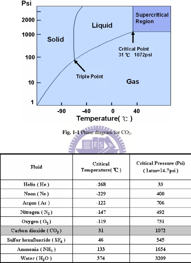
The supercritical fluid (SCF), which is exists above specific critical pressure and temperature, as shown in Fig 1-1 [15, 16]. It provides good liquid-like solvency and high gas-like diffusivity, giving it excellent transport capacity [17]. Table 1-1 shows critical pressure and temperature for some common fluids. CO2 is easy to acquire and safe to
be as supercritical fluid and it is easy to achieve supercritical state, low critical temperature (room temperature at 30℃) and not high critical pressure (1072psi = 72.8 atm), non-toxic, non-flammable, and inexpensive. The oxidant is also easily dissolved in SCCO2 fluid with specific surfactants. Thereby, we choose SCCO2 fluid to
transport the oxidant and penetrate the dielectric layer for trap passivation and interface oxidation at low temperature [18-20].
1.2 Motivation
To achieve a low temperature process on Ge-MOS device, high-k material is a good candidate to be gate dielectric for Germanium substrate. There are least four requirements to form gate dielectric on Germanium. First, the dielectric constant must be high (>20). Second, must be thermodynamic stable with Ge, the high-k material does not react with the Ge during depositing, to avoid a low-k interfacial layer formed during depositing, and make the dielectric constant of high-k material decrease. Third,
5
large enough band offset with Ge (>1eV), enough barrier high between Ge and gate dielectric can prevent the high leakage by carriers get thermal energy to overcome the barrier between Ge and gate oxide and to create leakage. Forth, form a good interface with Ge. The hafnium oxide (HfO2) and the zirconium oxide (ZrO2) are meeting the
above four conditions, and have been widely studied. For high-k metal gate, HfO2 is
widely used in 45nm processing. Because of it has better thermodynamic stability than ZrO2 on silicon. However, for germanium as the channel material, ZrO2 is more
compatible than HfO2, because of less interfacial layer which is low-k layer formed
after post-deposition annealing due to Ge intermixing in ZrO2 [21]. In addition, very
high-k (k~37) ZrO2 have been proposed via Ge incorporation into ZrO2[22]. Therefore,
ZrO2 is a good high-k material deposited on Ge, we choose ZrO2 as our research
high-k material.
Among several metal oxide films formations, in general, low temperature deposition is prefer, because of the low thermal budget and low costs. However, the low-temperature deposition films may cause poor interfacial properties with substrate and larger leakage current due to numerous traps inside the bulk metal oxide film. Proper annealing can reduced leakage and remove oxide charges and interface traps in the ZrO2. But for germanium substrate, the thermal stability of GeO2 is a critical
6
processes (like S/D annealing) could induce Ge decomposition into gate dielectric and increase leakage source enhance the leakage current after annealing. On my thesis, we use the low-temperature (100℃) technique supercritical fluid (SCF) to transport the oxidant and penetrate the dielectric layer for trap passivation and interface oxidation at low temperature. And by leakage current fitting to see how leakage mechanism transfers after SCF treats. Next, to repair the interface of ZrO2/Ge after SCF treatment
we use the Water Vapor Annealing. And then we combine these methods to form a good interface of ZrO2/Ge.
1.3 Organization of the Thesis
In chapter 2, we introduce the process flow of High-k on Germanium substrate Metal-Insulator-Semiconductor Capacitor (MIS-C) fabrication first. Second, the process instruments are introduced about RF-sputter, Vacuum Annealing Furnace, Rapid Thermal Annealing, Supercritical Fluid (SCF), Thermal coater. Third, electrical characteristics analysis instrument and material characteristics analysis instrument about X-ray Photoelectron Spectroscopy (XPS) and High-Resolution Transmission Electron Microscopy (HRTEM) are all introduced. Finally, the parameters extraction and transportation mechanism are also discussed in this chapter.
7
the ZrO2 film which deposited by sputter on Germanium substrate, then discussing the
thermal stability and the quality of high-k film. Then we accede Supercritical Fluid treatment(SCF) to our work and analyze in various electrical analysis techniques, such as capacitance-voltage (CV) and current density-voltage (JV) by Agilent 4980 and Keithley 4200 were perform to characteristic the device performance and analysis the interface and bulk quality of gate dielectric. For material analysis, such as x-ray photoelectron spectroscopy (XPS) and high-resolution transmission electron microscopy (HRTEM) to analyze variation of the interface after PDA and SCF.
On the second part, this section is continued from the preceding paragraph. First, we deposit the ZrO2 high-k gate dielectric on Ge substrates, and then anneal by using
rapid thermal annealing with wet nitrogen (with water vapor). The annealing in water vapor can suppress growth of unstable low-k GeOx interlayer in Ge
metal-oxide-semiconductor capacitor with high-k gate dielectric [23] by reducing the GeOx to Ge and through the low thermal budget process can repair the defect which
produced by reduction of GeOx in the interlayer. Second, to compare annealing with
and without water, we use the rapid thermal annealing with nitrogen to compare with water vapor annealing. By analyzing C-V and J-V curve which help us to understand the recovery of the defect in interlayer after GeOx reduction whether it need oxygen or
8
electron microscopy (HRTEM), x-ray photoelectron spectroscopy (XPS), were performed to characteristic the cross section of device and surface morphology. In the end, we combine the Supercritical Fluid treatment and water vapor annealing to form the device with good interface and low defect in the bulk high-k dielectric.
Finally, in chapter 4, we give the conclusions and suggestions of the thesis for the future work.
9
Fig. 1-1 Phase diagram for CO2.
10
Chapter 2
Experiment Instrument and Process
2.1 Experiment instrument of High-k on Germanium base
Metal-Insulator-Semiconductor Capacitor
2.1.1 RF Sputtering
Sputter deposition is a physical vapor deposition (PVD) method of depositing thin films by sputtering, that is ejecting, material from a "target," that is source, which then deposits onto a "substrate," such as a silicon wafer. Resputtering is re-emission of the deposited material during the deposition process by ion or atom bombardment. Sputtered atoms ejected from the target have a wide energy distribution, typically up to tens of eV (100,000 K). The sputtered ions (typically only a small fraction — order 1% — of the ejected particles are ionized) can ballistically fly from the target in straight lines and impact energetically on the substrates or vacuum chamber (causing resputtering). Alternatively, at higher gas pressures, the ions collide with the gas atoms that act as a moderator and move diffusively, reaching the substrates or vacuum chamber wall and condensing after undergoing a random walk. The entire range from high-energy ballistic impact to low-energy thermalized motion is accessible by changing the background gas pressure. The sputtering gas is often an inert gas such as argon. For efficient momentum transfer, the atomic weight
11
of the sputtering gas should be close to the atomic weight of the target, so for sputtering light elements neon is preferable, while for heavy elements krypton or xenon are used. Reactive gases can also be used to sputter compounds. The compound can be formed on the target surface, in-flight or on the substrate depending on the process parameters. The availability of many parameters that control sputter deposition make it a complex process, but also allow experts a large degree of control over the growth and microstructure of the film. Charge build-up on insulating targets can be avoided with the use of RF sputtering where the sign of the anode-cathode bias is varied at a high rate, as Fig. 2-1. RF sputtering works well to produce highly insulating oxide films but only with the added expense of RF power supplies and impedance matching networks. Stray magnetic fields leaking from ferromagnetic targets also disturb the sputtering process. Specially designed sputter guns with unusually strong permanent magnets must often be used in compensation.
12
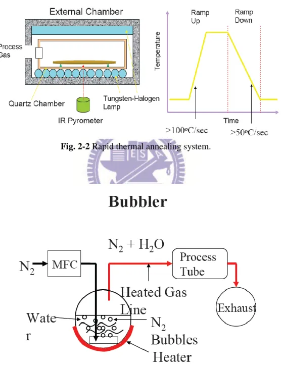
2.1.2 Water Vapor Rapid Thermal Annealing System
Rapid Thermal Anneal (RTA) is a subset of Rapid Thermal Processing as Fig. 2-2. It is a process used in semiconductor device fabrication which consists of heating a single wafer at a time in order to affect its electrical properties. Unique heat treatments are designed for different effects. Wafers can be heated in order to activate dopants, change film-to-film or film-to-wafer substrate interfaces, density deposited films, change states of depositing films, repair damage from ion implantation, move dopants or drive dopants from one film into another or from a film into the wafer substrate. Rapid thermal anneals are performed by equipment that heats a single wafer at a time using either lamp based heating, a hot chuck, or a hot plate that a wafer is brought near. Unlike furnace anneals they are short in duration, processing each wafer in several minutes. To achieve short time annealing time trade off is made in temperature and process uniformity, temperature measurement and control and wafer stress as well as throughput. And it can change the input gas to achieve different thermal treatment, even water vapor system, Fig. 2-3. Recently, RTP-like processing has found applications in another rapidly growing field — solar cell fabrication. RTP-like processing, in which an increase in the temperature of the semiconductor sample is produced by the absorption of the optical flux, is now used for a host of solar cell fabrication steps, including phosphorus diffusion for N/P junction formation
13
and impurity gettering, hydrogen diffusion for impurity and defect passivation, and formation of screen-printed contacts using Ag-ink for the front and Al-ink for back contacts, respectively.
Fig. 2-2 Rapid thermal annealing system.
14 2.1.3 Supercritical Fluid System
Supercritical fluid (SCF) is compound above their critical temperatures and pressure, as shown in Fig 1-1. [15, 16] The attractiveness of supercritical fluid for commercial applications is their unique combination of liquid-like and gas-like properties. The supercriticality is a strange and intriguing state in which solids can dissolve in gases, and liquids can alternate between reflectivity and transparency. The critical temperature and pressure for some common supercritical fluids are displayed in Table 1-1. The CO2-based supercritical fluid is particularly attractive because CO2
is non-toxic, non-flammable, recyclable, and inexpensive and has a reasonably high solvent power for most organic components. Besides, its critical conditions are easily achievable with existing process equipment (31 °C, 1072 psi =72.8 atm).
Figure 2-5 shows the density-pressure-temperature surface for pure CO2. It can
be discovered that relatively small changes in temperature or pressure near the critical point, resulting in large changes in density. Table 2-1 shows the comparison of several physical properties of typical liquid, vapor, and supercritical fluid state for CO2. It
could be seen that supercritical CO2 (SCCO2) fluid possesses liquid-like density, so
that SCCO2 fluid is analogous with light hydrocarbon to dissolve most solutes and
15
gas-like characteristic due to their viscosity and surface tension are extremely low, it allows SCCO2 fluid to keep superior diffusion capability than liquid to enter the
nano-scale dimension, as shown in Fig. 2-7. These properties are the reasons for SCCO2 fluid to employ in many commercial applications, including the extraction of
caffeine from coffee, fats from foods, and essential oils from plants for using in perfumes. Furthermore, in recent years, many records were investigated with SCCO2
fluid to apply in semiconductor fabrication by means of its high mass transfer rates and infiltration capabilities to clean wafer, strip photoresist, repair low-k material
[25-29]
. Figure 2-8 is the Scanning Electron Microscope (SEM) image of removing photoresist and photoresist residue from ion implant wafers. To put it briefly, SCCO2
fluid is one of the green solvents and suitable for the fabrication of nano-structure devices.
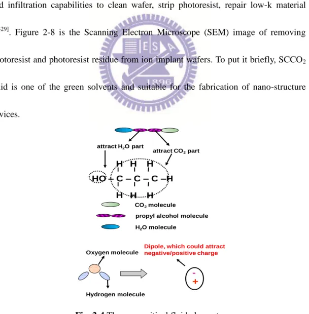
Fig. 2-4 The supercritical fluid element.
CO2molecule H2O molecule attract H2O part attract CO2part HO – C – C – C –H H H H H H H
propyl alcohol molecule
Oxygen molecule
Hydrogen molecule
+
-Dipole, which could attract negative/positive charge
16
Fig. 2-5 Density-pressure-temperature surface for pure CO2.[25]
17
Tab. 2-1 Comparison of physical properties of CO2.[26]
Fig. 2-7 Schematic of cleaning high aspect ratio structures with liquids and
supercritical fluids.
contamination
contamination
liquids
liquids
SCFs
SCFs
Cleaning with Cleaning with liquids liquids Cleaning with Cleaning with SCFs SCFscontamination
contamination
contamination
contamination
liquids
liquids
liquids
liquids
SCFs
SCFs
SCFs
SCFs
Cleaning with Cleaning with liquids liquids Cleaning with Cleaning with SCFs SCFs18
2.2 Process Flow of Zirconium Oxide on Germanium Substrate
Metal-Insulator-Semiconductor Capacitor (MIS-C) Fabrication
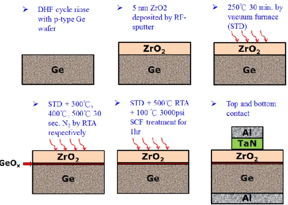
A 0.003 ohm-cm p-type (100) Ge wafer was cleaned with cycling DHF clean process and immediately loaded into the sputter chamber. As the chamber pressure reached to the 2×10⁻⁶ torr, about 5nm ZrO2 film was deposited by RF-sputter.
First, the sample was subjected to the post deposition annealing, first under 250°C for 30min in high vacuum furnace to be the STD sample, and then anneal with 300°C、 400°C and 500°C for 30sec by rapid temperature annealing (RTA) in nitrogen environment, separately. The SCF treatment was performed right after the 500°C RTA to repair the device performance. The sample was placed in a SCF system at 100°C for 1 hr, where was injected with 3000 psi of SCCO2 fluid that were mixed with 10
vol.% of propyl-alcohol and 10 vol.% of DI water. Finally, deposit 100nm tantalum-nitride electrodes by sputter and 500nm aluminum electrodes by thermal evaporation on the top surface of ZrO2 film with two electrode areas of 3.14×10⁻⁴ cm2
and 2.83×10⁻³ cm2, then BOE the back side of germanium wafer and deposit 500nm aluminum as back electrodes to fabricate MOS capacitors. The experiment flows of ZrO2/Ge capacitor with various treatments are exhibited in Fig. 2-8.
19
DHF clean process and immediately loaded into the sputter chamber. As the chamber pressure reached to the 2×10⁻⁶ torr, about 5nm ZrO2 film was deposited by RF-sputter.
There are two environment for rapid thermal annealing, first, the sample was annealed by using rapid thermal annealing in wet nitrogen (with water vapor) environment with 300°C for 3mins. Another is annealing in dry nitrogen environment without oxygen with 300°C for 3mins. Finally, deposit 100nm tantalum-nitride electrodes by sputter and 500nm aluminum electrodes by thermal evaporation on the top surface of ZrO2
film with two electrode areas of 3.14×10⁻⁴ cm2 and 2.83×10⁻³ cm2, then use BOE to the back side of germanium wafer and deposit 500nm aluminum as back electrodes to fabricate MOS capacitors. The experiment flows of ZrO2/Ge capacitor with various
treatments are also exhibited in Fig. 2-9.
In the end, we combine this two methods Supercritical Fluid treatment and water vapor annealing to form the device with good interface and low defect in the bulk high-k dielectric. First, we deposit about 5nm ZrO2 film on Ge substrate by RF-sputter,
and then anneal with 500°C for 30sec by Rapid Temperature Annealing (RTA) in nitrogen environment. Second, we use the Supercritical Fluid treatment (SCF) with 100°C and 3000psi for 1hr, and then anneal with 300°C for 3min by Rapid Temperature Annealing (RTA) in wet nitrogen environment (water vapor and nitrogen). The last, we deposit 100nm tantalum-nitride electrodes by sputter and
20
500nm aluminum electrodes by thermal evaporation on the top surface of ZrO2 film
21
Fig. 2-8 The experiment flows of ZrO2/Ge capacitor with different PDA treatment and SCF treatment.
22
2.3 Analysis Methods
2.3.1 Methods of Electrical Characteristics
2.3.1.1 Parameter Description
There are three parameters represent the characteristics of MOS capacitors.
Effective Oxide Thickness (EOT)
(2-1)
(2-2)
Eq. (2-1) represents the gate oxide capacitanceequivalent thickness of the SiO2,
Eq. (2-2) represents the effective oxide thickness (EOT) related to the dielectric constant of ZrO2. For the Eq. (2-2), the less EOT represents the value of k is higher.
Where εSiO2 is dielectric constant of SiO2, εZrO2 is dielectric constant of ZrO2, dthick is
thickness of ZrO2.
Flat Band Voltage (Vfb)
(2-3)
Eq. (2-3) represents the number of charge exists inside the dielectric, that means the Vfb near the zero bias, the less oxide charges existing inside the dielectric. Where
2 2 . SiO ZrO ox thick A A C EOT d 2 2 . SiO thick ZrO EOT d o FB ms ox Q V C
23
φms is the work function difference between gate and substrate, Q0 is the number of
oxide charges in the dielectric. Hysteresis (△Vfb)
Hysteresis represents the quality of interface between the dielectric and substrate, smaller △Vfb indicate better interface quality.
2.3.2 Methods of Material analysis
2.3.2.1 X-ray Photoelectron Spectroscopy
X-ray photoelectron spectroscopy (XPS) is a quantitative spectroscopic
technique that measures the elemental composition, empirical formula,chemical state and electronic state of the elements that exist within a material. XPS spectra are obtained by irradiating a material with a beam of X-rays while simultaneously measuring the kinetic energy and number of electrons that escape from the top 1 to 10 nm of the material being analyzed. XPS requires ultra high vacuum (UHV) conditions. XPS is a surface chemical analysis technique that can be used to analyze the surface chemistry of a material in its "as received" state, or after some treatment, for example: fracturing, cutting or scraping in air or UHV to expose the bulk chemistry, ion beam etching to clean off some of the surface contamination, exposure
24
to heat to study the changes due to heating, exposure to reactive gases or solutions, exposure to ion beam implant, exposure to ultraviolet light.
XPS is also known as ESCA, an abbreviation for Electron Spectroscopy for
Chemical Analysis.
XPS detects all elements with an atomic number (Z) of 3 (lithium) and above. It cannot detect hydrogen (Z = 1) or helium (Z = 2) because the diameter of these orbital is so small, reducing the catch probability to almost zero.
XPS is used to measure:
elemental composition of the surface (top 1–10 nm usually)
empirical formula of pure materials
elements that contaminate a surface
chemical or electronic state of each element in the surface
uniformity of elemental composition across the top surface (or line profiling or mapping)
uniformity of elemental composition as a function of ion beam etching (or depth profiling)
25
2.3.2.2 High-Resolution Transmission Electron Microscopy
High-resolution transmission electron microscopy (HRTEM) is an imaging mode of the transmission electron microscope (TEM) that allows the imaging of the crystallographic structure of a sample at an atomic scale. Because of its high resolution, it is an invaluable tool to study nano-scale properties of crystalline material such as semiconductors and metals. At present, the highest resolution realized is 0.8 angstroms (0.08 nm) with microscopes. Ongoing research and development such as efforts in the framework of TEAM will soon push the resolution of HRTEM to 0.5 Å . At these small scales, individual atoms and crystalline defects can be imaged. Since all crystal structures are 3-dimensional, it may be necessary to combine several views of the crystal, taken from different angles, into a 3D map. This technique is called electron crystallography. One of the difficulties with HRTEM is that image formation relies on phase-contrast. In phase-contrast imaging, contrast is not necessarily intuitively interpretable as the image is influenced by strong aberrations of the imaging lenses in the microscope. One major aberration is caused by focus and astigmatism, which often can be estimated from the Fourier transform of the HRTEM image.
26
Chapter 3
Results and Discussion
3.1 Effect of Supercritical Fluid and Post-Deposition Annealing on
the ZrO
2/Ge MOS-Capacitor
This section we investigate the effect of Supercritical Fluid treatment (high-pressure H2O treatment) on the sputter-deposition of ZrO2/Ge stack. Then
analysis of electrical characteristics can examine the quality of the treated device, and the material analysis of X-ray photoelectron spectroscopy (XPS) and high-resolution transmission electron microscopy (HRTEM) reveal the situation of interfacial GeOx
between ZrO2 and Ge which is a redox of ZrO2 with H2O and GeOx with H2,
including the bonding of Zr and Ge with O, and real thickness of GeOx. The
suppression of GeOx interlayer between ZrO2 and Ge substrate can decreases the gate
leakage current effectively.
3.1.1 Thermal Stability of ZrO2/Ge MOS-Capacitor
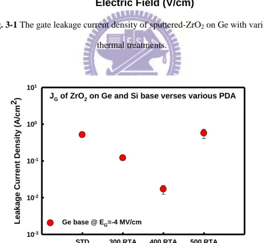
The thermal stability of MOS-C is the most important norm to referee quality of MOS-C. In the Fig. 3-1, it represents the variation of gate leakage current density (JG)
27
ZrO2 on p-type Ge substrate at negative and positive electrical field is due to fast
generation rate of minority carrier. Furthermore, the JG of ZrO2/Ge capacitor
decreases with increasing annealing temperature until 400 °C and then increases at 500 °C, as shown in Fig. 3-2. The high and unstable JG of ZrO2/Ge capacitor may be
related to formation, decomposition and amalgamation of the Ge oxide during thermal process. The JG comparison of depositing ZrO2 on Ge has the same trend which the JG
increases after 500 °C thermal process due to the thermal decomposition GeOx into
dielectric.
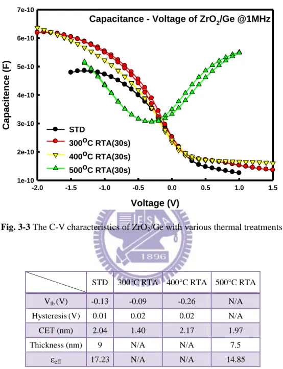
The C-V characteristics of ZrO2/Ge capacitor which treated by various thermal
treatments are shown in Fig. 3-3 and the parameters are extracted in Table 3-1. The Vfb, Hysteresis, Thickness, CET and εeff present flat-band voltage, shift of flat-band
voltage, thickness of ZrO2 measured by n-k instrument, capacitance effective
thickness and effective dielectric permittivity, respectively. We can know the lower accumulation capacitance in standard condition and 500 °C RTA-treated condition are attributed to the bad quality of ZrO2 layer, because of its poor charge holding ability
and cause high gate leakage, as shown in Fig. 3-3. Besides, the response of inversion capacitance at positive bias in 500 °C RTA-treated condition is expressed poor interface quality between ZrO2 and Ge substrate. On the other hand, when
28
ZrO2/Ge capacitor is improved. But we know the activation temperature of
source/drain annealing in the MOS process always be above 500 °C. Therefore, how to repair the thermal damage in gate dielectric and interface for Ge-based MOS device is necessary. So we bring up an idea about Supercritical Fluid treatment (high-pressure H2O treatment) to repair the thermal damage of gate dielectric and
29
Gate Leakage Current Density of ZrO2/Ge
Electric Field (V/cm)
-4x10⁶ -3x10⁶ -2x10⁶ -1x10⁶ 0 1x10⁶ 2x10⁶ 3x10⁶ 4x10⁶Lea
ka
ge Cur
re
nt Dens
ity
(A/cm
2
)
10-9 10-8 10-7 10-6 10-5 10-4 10-3 10-2 10-1 100 101 STD 300oC RTA (30s) 400oC RTA (30s) 500oC RTA (30s)Fig. 3-1 The gate leakage current density of sputtered-ZrO2 on Ge with various thermal treatments.
JG of ZrO2 on Ge and Si base verses various PDA
STD 300 RTA 400 RTA 500 RTA
Leakage C urr ent D ensity (A/ cm 2 ) 10-3 10-2 10-1 100 101 Ge base @ EG=-4 MV/cm
Fig. 3-2 The gate leakage current density of sputtered-ZrO2 on Si with various
30
Capacitance - Voltage of ZrO2/Ge @1MHz
Voltage (V) -2.0 -1.5 -1.0 -0.5 0.0 0.5 1.0 1.5 C ap ac ite nc e (F) 1e-10 2e-10 3e-10 4e-10 5e-10 6e-10 7e-10 STD 300oC RTA(30s) 400oC RTA(30s) 500oC RTA(30s)
Fig. 3-3 The C-V characteristics of ZrO2/Ge with various thermal treatments.
Table 3-1 The parameter of C-V characteristics for ZrO2/Ge with various thermal
treatments.
STD 300°C RTA 400°C RTA 500°C RTA
Vfb (V) -0.13 -0.09 -0.26 N/A
Hysteresis(V) 0.01 0.02 0.02 N/A
CET (nm) 2.04 1.40 2.17 1.97
Thickness (nm) 9 N/A N/A 7.5
31
3.1.2 Effect of Supercritical Fluid Treatment on ZrO2/Ge MOS-C
To repair the thermal damage in gate dielectric and interface for Ge-based MOS device, we propose an idea about Supercritical Fluid Treatment (SCF) as high pressure water treatment. The purpose of our treatment will focus on the interface of ZrO2/Ge device.
First, the electrical characteristics are shown in Fig. 3-4, presenting the JG with
and w/o SCF treatment after 500 °C RTA treatment (serious thermal damage). It surely works to decrease the gate leakage about 3 orders after 500 °C RTA thermal damage. The cross-sectional HRTEM images in Fig. 3-5 show the sputtered ZrO2 on
Ge substrate after high vacuum annealing treat at 250 oC w/o and with N2 RTA at
500 oC for 30s, then in Fig. 3-6 show the sputtered ZrO2 on Ge substrate after N2 RTA
treat at 500 oC for 30s w/o and with SCF treatment. After thermal process, the ZrO2
film crystallizes clearly, and the thickness of GeOx layer decrease with high
temperature RTA. The 4 and 2.5 nm-thickness GeOx layers are observed w/o and with
RTA, respectively, and effect of the SCF treatment on GeOx was discovered by
HRTEM images in Fig. 3-6 (b) without GeOx interfacial layer amazingly.
Second, from the Fig. 3-7 and Fig. 3-8, the XPS spectra of Ge 2p3/2 and Zr 3p3/2
32
reaction between ZrO2 and GeOx is existent during RTA and SCF treatment. The Ge
2p3/2 peak at binding energies about 1217 eV and 1219.4 eV are associated with pure
Ge and GeOx, respectively, shown in Fig. 3-7.[30] And the interfacial layer of STD and
500 °C RTA treated is almost GeOx, but it will be removed after SCF treatment. Then,
the Zr 3p3/2 peak at a binding energy about 332.5 eV is associated with ZrO2, and
shown in Fig. 3-8. The peak of Zr 3p3/2 signal which is treated by SCF treatment shift
to higher binding energy as the Ar+ sputtering time increases, but not obvious in the STD and RTA-treated condition.
Base on the previous evidences, we can know that the zirconia will be oxidized more when the GeOx eliminated by SCF treatment, and cause JG decrease. For the
elimination of GeOx layer, it called reduction of GeOx. The redox may occur at the
interface between ZrO2 and GeOx during SCF treatment, as follows:
Zr + 2H2O ZrO2 + 2H2 (3-1)
GeO + H2 Ge + H2O (3-2)
The reactions imply the H2O is taken as oxidant and reacts with the non-oxidized Zr
in the interlayer and the GeOx dissolved after SCF treatment. The amounts of ionic
products which are like H3O+ and OH- radicals in H2O at high pressure may higher
than those obtained in atmospheric pressure. The higher amounts of free radicals are associated with a strengthened oxidation reaction between H2O and non-oxidized Zr
33
owing to the higher collision frequency, as Eq. (3-1).[31] Besides, the generation of hydrogen using Zr and H2O has also been reported.[32] The existence of H2, the
reaction of Eq. (3-2) proceeds spontaneously (ΔG=-42.69 kJ/mol at 100oC) and reduces the GeOx to Ge.[33] In addition, Zr oxidation reacts easilyat the interface of
ZrO2/Ge due to the H2 is effectively removed by GeOx. Therefore, SCF treatment can
eliminate the interfacial GeOx layer in the ZrO2/Ge effectively. The transporting
mechanism of SCF elements may diffuse through the grain boundary of poly-type ZrO2 film, as the Fig. 3-9, and the schematic diagram of GeOx reduction reactions is
in the Fig. 3-10.
In the end, it’s clearly to know the reduction of GeOx by depth profiles of Zr, O
and Ge atoms in Fig. 3-11 to Fig. 3-13. The depth profiles are analyzed by collecting XPS signals with various Ar+ sputtering time. Singnals of O 1s, Zr 3p3/2 and Ge 2p3/2
were collected to calculate the atom %. From the Fig. 3-11 to Fig. 3-13, the amount of GeOx decrease by thermal process which the following RTA in N2 ambient at 500 °C
for 30s. This is the thermal decomposition of GeOx when the temperature of annealing
is higher than 420 °C.[34] In the Fig. 3-13, we know SCF treatment can cause the interfacial GeOx signal to vanish and reduced the amount of GeOx that was
incorporated into the ZrO2 thin film. So, the SCF treatment can eliminate the amount
34
Gate Leakage Current Density of ZrO2/Ge
Electric Field (V/cm)
-4e+6 -3e+6 -2e+6 -1e+6 0 1e+6 2e+6 3e+6 4e+6
Lea ka ge Cur re nt Dens ity (A/cm 2 ) 1e-9 1e-8 1e-7 1e-6 1e-5 1e-4 1e-3 1e-2 1e-1 1e+0 1e+1 500oC RTA (30s) 500oC RTA (30s)+SCF
Fig. 3-4 The gate leakage current density of 500℃ RTA-treated condition on Ge with
35
Fig. 3-5 The cross-sectional HRTEM images of sputtered-ZrO2 on Ge with high vacuum annealing at 250 oC (a) w/o and (b) with RTA treatment at 500 oC.
Fig. 3-6 The cross-sectional HRTEM images of sputtered-ZrO2 on Ge with high vacuum annealing at 250 oC and 500 oC RTA (a) w/o and (b) with SCF treatment.
36
Binding Energy [eV]
1214 1216 1218 1220 1222 1224 Ge 2p 3 /2 photoelectr on inte nsity [a .u. ] Ge 2p3/2 0.2m 0.4m 0.6m 0.2m 0.4m 0.6m 0.2m 0.4m 0.6m sputter time GeOx STD 500oC RTA (30s) 500oC RTA+SCF XPS of Ge 2p3/2
Fig. 3-7 The XPS spectra of Ge 2p3/2 with various treatments.
Binding Energy [eV]
328 330 332 334 336 338 Zr 3p 3 /2 photoelectr on inte nsity [a .u. ] ZrOx 0.8m 0.2m 0.4m 0.6m 0.8m 0.2m 0.4m 0.6m 0.8m 0.2m 0.4m 0.6m sputter time Ge Auger peak STD 500oC RTA (30s) 500oC RTA (30s) + SCF XPS of Zr 3p3/2
high binding energy shift
Fig. 3-8 The XPS spectra of Zr 3p3/2 with various treatments.
37
Fig. 3-9 The transporting mechanism for SCCO2 fluids taking H2O molecule into
dielectric film.
38
Fig. 3-11 Depth profiles of Zr, O and Ge atoms in ZrO2/Ge after high vacuum annealing at 250 °C for 30 min by XPS.
39
Fig. 3-12 Depth profiles of Zr, O and Ge atoms in ZrO2/Ge after high vacuum annealing at 250 °C for 30min and 250 °C RTA for 30sec by XPS.
40
Fig. 3-13 Depth profiles of Zr, O and Ge atoms in ZrO2/Ge after high vacuum annealing at 250 °C for 30 min, 250 °C RTA for 30sec and SCF for 60min by XPS.
41
3.2 Effect of Water Vapor Annealing on the ZrO
2/Ge MOS-
Capacitor
Continued from the preceding section,this section we investigate the effect of Water Vapor Annealing (atmospheric pressure H2O treatment) on the
sputter-deposition of ZrO2/Ge stack. The differences between Water Vapor Annealing
and Supercritical Fluid Treatment are different treated pressure and temperature. After suitable annealing temperature with water vapor, it can also reduce GeOx layer and
repair the defect which formed by reduction of GeOx effectively. And then analysis of
electrical characteristics can examine the quality of the treated device, and the material analysis of X-ray photoelectron spectroscopy (XPS) reveal the situation of interfacial GeOx between ZrO2 and Ge which is a redox of ZrO2 with H2O and GeOx
with H2, including the bonding of Zr and Ge with O, and real thickness of GeOx.
3.2.1 Compare with Water Vapor Annealing and Nitrogen Annealing
After Supercritical Fluid Treatment (SCF), it may leave many defects on the interface of ZrO2/Ge and cause poor C-V characteristics. To solve this problem, we
propose an idea about water treatment with suitable temperature (below 420oC), called Water Vapor Annealing. The purpose of our treatment will focus on the repair
42
of ZrO2/Ge interface.
First, the electrical characteristics are shown in Fig. 3-14, presenting the JG with
Water Vapor Annealing and Dry Nitrogen Annealing at 300 °C for 3min. The JG of
H2O+N2 300 °C RTA is lower than dry N2 300 °C RTA, because the suppression of
the GeOx causes fewer interface traps. [23] In the C-V characteristics, they are shown in
Fig. 3-17. The accumulation capacitance of H2O+N2 RTA is higher than dry N2 RTA
at 300oC, because of the H2O+N2 300 °C RTAcan reduce the GeOx layer and the total
thickness is thinner than dry N2 300 °C RTA. Besides, form slope of the depletion
capacitance, the slope of H2O+N2 300 °C RTA is sharper than dry N2 300 °C RTA, it
indicates the interface quality of H2O+N2 300 °C RTA is better than dry N2 300 °C
RTA, and this should be attributed to the suppressed growth of the unstable GeOx
interlayer by water treatment. As the following material analysis, there is more evidence to prove the water treatment can suppress the growth of the unstable GeOx
interlayer and form superior bulk and interface properties.
Second, from the Fig. 3-16 and Fig. 3-17, the XPS spectra of Ge 2p3/2 and Zr
3p3/2 shows the bonding situations and composition respectively. We detect that the
reaction between ZrO2 and GeOx is existent during 300oC H2O+N2 and dry N2 RTA.
The Ge 2p3/2 peaks of 300oC H2O+N2 RTA and dry N2 RTA at binding energies about
43
Fig. 3-16. The ratio of GeOx treated by dry N2 RTA is higher than H2O+N2 RTA, and
it means H2O treatment can eliminate GeOx layer. Comparing with SCF and H2O+N2
RTA, it’s clear to know high pressure water treatment can eliminate GeOx layer
effectively than atmospheric pressure water treatment, so the redox of water in high pressure is more efficacious than in atmospheric pressure. And a lot of defects in the GeOx layer will cause the high gate leakage, showed as the JG of H2O+N2 300 °C RTA
is lower than dry N2 300 °C RTA. [23] Then, the Zr 3p3/2 peak at a binding energy
about 332.5 eV is associated with ZrO2, and shown in Fig. 3-17. The peak of Zr 3p3/2
signals which is sample treated by H2O+N2 300 °C RTA shift to higher binding
energy as the Ar+ sputtering time increases, but not obvious in the STD and dry N2
300 °C RTA condition. It means that un-bonding Zr will oxidize by with the water treatment, so water treatment will cause redox surely.
In the end, it’s clearly to know the reduction of GeOx by depth profiles of Zr, O
and Ge atoms in Fig. 3-18, Fig. 3-19 and Fig. 3-20. The depth profiles are analyzed by collecting XPS signals with various Ar+ sputtering time. Singnals of O 1s, Zr 3p3/2 and
Ge 2p3/2 were collected to calculate the atom %. From the Fig. 3-18 to Fig. 3-20, the
amount of GeOx decrease by H2O+N2 300 °C RTA for 3min, but not dry N2 300 °C
RTA. In the Fig. 3-19, we know water treatment can reduce the amount of GeOx
44
temperature, showed as C-V characteristics in Fig. 3-15. So, the SCF treatment can eliminate the amount of GeOx more effectively and help to reduce the gate leakage
45
Gate Leakage Current Density of ZrO2/Ge
Electric Field (V/cm)
-2e+6 -1e+6 0 1e+6 2e+6
Le
a
k
a
ge
Cur
re
nt De
ns
ity
(A/c
m
2
)
10-7 10-6 10-5 10-4 10-3 10-2 10-1 100 101 102 STD300oC H2O RTA 300oC N2 RTA
Fig. 3-14 The gate leakage current density of ZrO2/Ge with 300oC H2O and N2 RTA.
Capacitance - Voltage of ZrO2/Ge @1MHz
Voltage (V)
-1.5 -1.0 -0.5 0.0 0.5 1.0 1.5Capac
itence (F)
0 1e-10 2e-10 3e-10 4e-10 5e-10 6e-10 7e-10 8e-10 STD300oC H2O RTA 300oC N2 RTA
46
Binding Energy [eV]
1214 1216 1218 1220 1222 1224 Ge 2p 3 /2 photoelectr on inte nsity [a .u. ] Ge 2p3/2 0.4m 0.5m 0.6m 0.4m 0.5m 0.6m 0.4m 0.5m 0.6m sputter time GeOx STD 300oC H2O RTA 300oC N2 RTA XPS of Ge 2p3/2
Fig. 3-16 The XPS spectra of Ge 2p3/2 with 300oC H2O and N2 RTA.
Binding Energy [eV]
328 330 332 334 336 338 Zr 3p 3 /2 photoelectr on inte nsity [a .u. ] ZrOx 0.4m 0.1m 0.2m 0.3m 0.4m 0.1m 0.2m 0.3m 0.4m 0.1m 0.2m 0.3m sputter time STD 300oC H2O RTA 300oC N2 RTA XPS of Zr 3p3/2
high binding energy shift
47
Sputter time (min)
0.0
0.5
1.0
1.5
2.0
Ato
m
(
%
)
0
20
40
60
80
100
Zr GeOx Ge OZrO
2/Ge
(STD)
Fig. 3-18 Depth profiles of Zr, O and Ge atoms in ZrO2/Ge with STD condition by XPS.
48
Sputter time (min)
0.0
0.5
1.0
1.5
2.0
Ato
m
(
%
)
0
20
40
60
80
100
Zr
GeO
xGe
O
ZrO
2/Ge
(300
oC H
2O RTA)
Fig. 3-19 Depth profiles of Zr, O and Ge atoms in ZrO2/Ge with Water Vapor Annealing at 300 °C for 3 mins by XPS.
49
Sputter time (min)
0.0
0.5
1.0
1.5
2.0
Ato
m
(
%
)
0
20
40
60
80
100
Zr GeOx Ge OZrO
2/Ge
(300
oC N
2RTA)
Fig. 3-20 Depth profiles of Zr, O and Ge atoms in ZrO2/Ge with Dry Nitrogen Annealing at 300 °C for 3 mins by XPS.
50
3.2.2 Combination of Supercritical Fluid and Water Vapor Annealing
Continued from the preceding sections, the water treatment is effective in reduction of GeOx, and through suitable annealing temperature can repair the defect
of interface by reducing GeOx. In the Fig. 3-21, it shows that the accumulation
capacitance of sample treated by SCF and Water Vapor Annealing will return to STD, and more higher than treated by Water Vapor Annealing only. Therefore, the SCF can reduce the GeOx effectively but it also leave defect on the interface, and cause the
poor C-V characteristic. To solve this problem the Water Vapor Annealing is good for repair the interface by suitable temperature (below 420oC), and the water can also prevent the production of GeOx, so the C-V characteristic can return to STD after
thermal treatment. In addition, the SCF can enhance the electric characteristic obviously after the thermal process only, and it doesn’t work without any thermal process first due to the degree of dielectric crystallization. The degree of dielectric crystallization may help the SCF element diffuse into dielectric more easily.
51
Capacitance - Voltage of ZrO2/Ge @1MHz
Voltage (V) -1.5 -1.0 -0.5 0.0 0.5 1.0 1.5 C a pa c ite nc e (F) 0 1e-10 2e-10 3e-10 4e-10 5e-10 6e-10 7e-10 8e-10 STD
300oC H2O RTA 500oC RTA + SCF + 300oC H2O RTA
Fig. 3-21 The C-V characteristics of ZrO2/Ge with combining SCF and 300oC H2O
RTA.
3.3 Summaries
In the summary, the growth of the unstable GeOx interlayer by the thermal
process can be suppressed by the water treatment. No matter the water at high pressure or atmospheric pressure, it all can eliminate the GeOx interlayer and suppress
the growth of GeOx. But it’s clear to know the pressure of the water treatment effect
the capability of redox. In terms of the depth profiles analyzed by XPS and HRTEM images, the amount of GeOx by treating with high pressure water treatment is less
52
can reduce the gate leakage current effectively, and annealing with the suitable temperature can also repair the defect of interface.
53
Chapter 4
Conclusions and Future works
4.1 Conclusions
In this study, to solve the thermal decomposition of GeOx the high pressure water
treatment (supercritical fluids technology) is employed originally to eliminate the GeOx interlayer and improve the properties of ZrO2 high-k film. First, the thermal
stability of ZrO2/Ge stack is analyzed by the sample treated with 250oC high vacuum
furnace annealing for 30min and then treated by 300oC, 400oC and 500oC N2 RTA for
30s respectively. Second, the high pressure water treatment (SCF) at 100oC and 3000psi for 1hr used to the sample which is treated by 500oC N2 RTA for 30s. By
HR-TEM, XPS analyses, it can verify the elimination of GeOx interlayer due to the
SCF treatment surely, and explain the improvement of the gate leakage after SCF treatment. We also indicate the mechanism about the reduction of GeOx interlayer in
ZrO2/Ge by SCF treatment, including the oxidation of un-bonding Zr and reduction of
GeOx. The reduction of GeOx layer at the ZrO2/Ge interface can reduce the interface
defects and cause the gate leakage decrease. Besides, the Water Vapor Annealing is used to verify the water treatment has the ability of redox in the ZrO2/Ge stack, and
54
though the annealing by suitable temperature can repair the interface to improve the electric characteristic of ZrO2/Ge device.
The water treatment with suitable annealing temperature is the attractive technology to apply on Ge-typed MOS devices process. It’s useful to resolve the GeOx thermal decomposition issues to repair the interface of device which treated by
thermal process and fabricate the high quality Ge-typed MOS devices.
4.2 Future works
To complete the high quality Ge-MOSFET, metal gate is another issue on the
germanium devices. The work function tuning is a key to determined threshold voltage, however, for Ge-MOSFET, Fermi level pinning is the problem on metal gate/ high-k/Ge MOS stack devices, which is waiting to be solved.
The feasibility of SCF can join the suitable temperature (below 400oC), and two step annealing to form the good interface, no GeOx interlayer and good dielectric
quality of high-k/Ge MOS stack. First, low temperature (below 300oC) annealing with high vacuum system. Second, after high temperature process, SCF treatment with suitable annealing temperature can eliminate the GeOx interlayer which formed by
55
Reference
[1] S. M. Sze, and Kwok K. Ng, Physics of Semiconductor Devices 3rd. [2] E. J. Nowak, IBM J. Res. & Dev. Vol. 46 No. 2/3, 2002.
[3] K. Rim, S. Koester, M. Hargrove, J. Chu, P. M. Mooney, J. Ott,T. Kanarsky, P.Ronsheim, M. Ieong, A. Grill, and H.-S. P. Wong, Symposium on VLSl
Technology Digest of Technical Papers, pp.59-60, 2001.
[4] M. L. Lee, Eugene A. Fitzgerald, Mayank T. Bulsara, Matthew T. Currie, and Anthony Lochtefeld, J. Appl. Phys. Vol. 97, 011101, 2005
[5] Scott E. Thompson, Robert S. Chau, Tahir Ghani, Kaizad Mistry, Sunit Tyagi, and Mark T. Bohr, IEEE T. Semiconduct. M. Vol. 18, No. 1, pp. 26, 2005
[6] X. Huang, W.-C. Lee, C. Kuo, D. Hisamoto, L. Chang, J. Kedzierski, E. Anderson, H. Takeuchi, Y.-K. Choi, K. Asano, V. Subramanian, T.-J. King, J. Bokor, and C. Hu, ―Sub 50-nm FinFET: PMOS,‖ IEEE T. Electron Dev. Vol. 48,
No. 5, pp. 880, 2001
[7] S. Takagia, T. Maeda, N. Taoka, M. Nishizawa, Y. Morita, K. Ikeda, Y. Yamashita, M. Nishikawa, H. Kumagai, R. Nakane, S. Sugahara and N. Sugiyama,
Microelectron. Eng. Vol. 84, pp.2314, 2007.
[8] Hiroshi Matsubara, Takashi Sasada, Mitsuru Takenaka, and Shinichi Takagi, Appl.
Phys. Lett. Vol. 93, 032104, 2008.
[9] K. Prabhakaran, F. Maeda, Y. Watanabe, and T. Ogino, Appl. Phys. Lett. Vol. 76,
2244, 2000.
[10] J. Oh and J. C. Campbell, J. Electron. Mater. Vol. 33, pp.364, 2004.
[11] S. Van Elshocht, B. Brijs, M. Caymax, T. Conard, T. Chiarella, S. De Gendt, B. De Jaeger, S. Kubicek, M. Meuris, B. Onsia, O. Richard, I. Teerlinck, J. Van


![Fig. 2-5 Density-pressure-temperature surface for pure CO 2 . [25]](https://thumb-ap.123doks.com/thumbv2/9libinfo/8761006.208178/29.892.155.744.149.995/fig-density-pressure-temperature-surface-pure.webp)
![Tab. 2-1 Comparison of physical properties of CO 2 . [26]](https://thumb-ap.123doks.com/thumbv2/9libinfo/8761006.208178/30.892.142.788.189.415/tab-comparison-physical-properties.webp)