Effect of low-temperature annealing on the luminescent lifetime and negative
differential resistance of silicon-implanted borosilicate glass
Gong-Ru Lin
Citation: Journal of Applied Physics 94, 7542 (2003); doi: 10.1063/1.1630366 View online: http://dx.doi.org/10.1063/1.1630366
View Table of Contents: http://scitation.aip.org/content/aip/journal/jap/94/12?ver=pdfcov
Published by the AIP Publishing
Articles you may be interested in
Effect of annealing on the structural and luminescent properties of ZnO nanorod arrays grown at low temperature
J. Appl. Phys. 109, 103508 (2011); 10.1063/1.3586243
Synthesis of In 2 O 3 nanocrystal chains and annealing effect on their optical properties
J. Vac. Sci. Technol. A 25, 1038 (2007); 10.1116/1.2710244
Structural and optical properties of Si Si O 2 superlattices prepared by low pressure chemical vapor deposition
J. Appl. Phys. 100, 013524 (2006); 10.1063/1.2210667
H-induced effects in luminescent silicon nanostructures obtained from plasma enhanced chemical vapor deposition grown Si y O 1 y : H ( y > 1 3 ) thin films annealed in ( Ar + 5 % H 2 )
J. Vac. Sci. Technol. A 24, 817 (2006); 10.1116/1.2177227
Defect-enhanced photoconductive response of silicon-implanted borosilicate glass
Appl. Phys. Lett. 85, 935 (2004); 10.1063/1.1779945
the redshifted photoluminescence共PL兲 interprets the change in category and the decrease in density of irradiative defects in BSO:Si⫹. Time-resolved PL analysis reveals a lengthening luminescent lifetime of BSO:Si⫹from 1.7 to 2.8 ns, which indicates that the density ratio of nonradiative defects in as-implanted BSO:Si⫹ are reduced by one-tenth after annealing for 60 min. Transmission line mode analysis shows that both the leakage current and the contact resistance of a metal– BSO:Si⫹–metal diode has dramatically changed by three orders of magnitude. A strong negative differential resistance 共NDR兲 and associated double-barrier electron tunneling phenomenon are observed with a threshold electric field of 290–350 kV/cm. The decreasing barrier height of the metal–BSO:Si⫹ junction from 3.0 to 1.9 eV is mainly contributed by deep-level defects with activation energy of ⬃1 eV. After annealing, the NDR effect significantly diminishes, the barrier height raises to⬎2.4 eV, and most electrical characteristics of the metal–BSO:Si⫹ junction have recovered back to be comparable with those of the metal–BSO junction due to the elimination of these defects. © 2003 American Institute of Physics. 关DOI: 10.1063/1.1630366兴
I. INTRODUCTION
Various fabricating technologies were developed in the past few years to synthesize the buried Si nanocrystal in glass, quartz, and thermal dioxide (SiO2) layer on Si
sub-strates, which have inspired enormous research on its struc-ture, electrical, and optical properties due to its potential ap-plications in optoelectronics.1–5The Si nanocrystal has been shown to exhibit relatively strong photo- and electro-luminescence 共PL and EL兲 from the blue-green to near-infrared wavelength region.6 Recently, the synthesis of Si nanocrystals via Si ion implantation has also caused consid-erable interest.7Song et al.8have reported the redshift in PL of Si ion-implanted SiO2(SiO2:Si⫹) films from 470 to 600
nm after annealing. Gazecki et al. have demonstrated the re-fractive index analysis of planar optical waveguides formed upon SiO2:Si⫹.
9
The Si nanocrystal has been employed not only for fabricating light emitting and guiding devices, but also for nanocrystallite memory devices and photoconduct-ing sensors. Not long ago, the inversion- and accumulation-mode gate current density of metal–oxide–semiconductor 共MOS兲 capacitors with a 50-nm-thick SiO2:Si⫹ layer with
doses from 1013 to 3⫻1016cm⫺2 have been studied.10 The
possible carrier transport mechanism has been referred to either as the Fowler–Nordheim 共FN兲 or the Poole–Frenkel 共PF兲 model.11–13 Furthermore, Rossi et al.14 has
character-ized optical and electrical properties of Si nanocrystals formed in continuous-wave argon-laser-treated and hydroge-nated amorphous SiOxalloys under different processing
con-ditions. The thermionic conductivity of the SiO2:Si⫹ has
indicated the existence of deep-level defects with an activa-tion energy of Ea⬵1 eV. Other anomalous electrical
phe-nomena such as variable-range hopping conduction was also found in Si-implanted Si or porous Si materials containing Si nanostructures.15,16 It was believed that the formation of Si nanocrystals could induce a dramatic change in the tempera-ture dependence of the conductivity. In addition, the negative differential resistance 共NDR兲 effect in, such as, SiOx,
17
single porous Si layer,18porous Si supperlattice,19and Al2O3 matrix with buried Si nanocrystals,20 have also been re-ported. The NDR-related resonant electron tunneling behav-ior has also been studied.21–23Nonetheless, the variation in the electrical properties of SiO2:Si⫹ annealed at low tem-perature conditions was less discussed in previous studies. In this article, the effect of low-temperature annealing on the defect-induced anomalous electrical characteristics of silicon-implanted borosilicate glass (BSO:Si⫹) is studied via the transmission line model 共TLM兲 analysis of metal-semiconductor metal 共MSM兲 diodes with various spacing made on as-implanted and annealed BSO:Si⫹substrates. The evolution in the NDR effect as well as the electron tunneling behavior, the contact and sheet resistances, the breakdown field, the saturation current, and the barrier height of the MSM diode made on BSO:Si⫹ annealed at different dura-tions are reported.
II. EXPERIMENT
The BSO:Si⫹samples were prepared by multiple-energy implanting the 125⫾20-m-thick BSO glass with Si ions at energies of 50, 100, and 200 keV under the same dosage of
a兲Electronic mail: [email protected]
7542
0021-8979/2003/94(12)/7542/5/$20.00 © 2003 American Institute of Physics
1016ions/cm2. The implanted depth profile of Si ions ob-tained by use of a Monte Carlo simulating program共TRIM兲 is
shown in Fig. 1. The encapsulated thermal annealing of BSO:Si⫹ samples was performed in a furnace with flowing nitrogen gas at 500 °C ranging from 30 to 120 min at 30 min increments. The structural property of the BSO:Si⫹ is char-acterized by x-ray diffraction 共XRD兲 with Cu K␣ radiation and room-temperature photoluminescence共PL兲 spectroscopy with an excitation wavelength of 360 nm. Nanosecond life-time measurements are achieved by using a commercially available time-resolved PL共referred as TRPL兲 system, which consists of a pulsed nitrogen lamp as the 350 nm wavelength excitation source and a photon counter共Edinburgh, FL900兲. The TRPL system has the spectral range, the pulse width, and the repetition rate ranging from 110 to 850 nm,⬃1 ns, and 40 kHz, respectively. The detection is performed by a cooled Hamamatsu GaAs photomultiplier tube 共PMT兲 con-trolled at ⫺22 °C. A time-correlated single-photon counting system is used to characterize the fluorescence lifetime of the BSO:Si⫹ sample at a wavelength of 500 nm. To investigate the NDR effect, 200-nm-thick Al electrodes for TLM analy-sis were fabricated with contact size and spacing of 75⫻50
m2 and ranging from 1 to 25 m, respectively. The current–voltage (I – V) measurements were performed using a programmable high-resistance meter 共Hewlett Packard HP4339B兲, in which the biased voltage of the BSO:Si⫹ MSM diode was scanned from 0 to 600 V at increments of 1 V. The entire scanning time for the I – V profile is 6 s, which corresponds to a ramp rate of 0.1 V/ms. After measuring the resistances (Ri) of SiO2:Si⫹ diodes with different contact
spacing (Li), the lateral contact resistance (Rc) and the sheet
resistance (Rs) can be evaluated from the intercept of
⫺2Rcw/Rsat the x axis and the intercept of 2Rcat the y axis
in the plot of Ri⫽2Rc⫹RsLi/W as a function of Li. The specific contact resistivity of the MSM diode made on BSO:Si⫹, c⫽W2Rc
2
/Rs can also be obtained.
III. RESULTS AND DISCUSSIONS
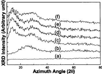
The XRD curve of BSO glass is significantly changed after Si implantation, as shown in Fig. 2. The as-implanted BSO:Si⫹ exhibits a relatively weak and broadened XRD peak at an azimuth angle of about 25° associated with its full-width at half-maximum 共FWHM兲 of about 14°. After
annealing for 30 min, the original XRD peal splits into two peaks located at angles of 14° and 29° with FWHM of 8° and 12°, respectively. The XRD peak at 2⫽29° is previously attributed to the recrystalization of 共111兲-oriented Si phases in the BSO:Si⫹ glass.17,18The other XRD peak centered at 2⫽14° considerably correlates with the gradually crystal-lized SiO2 matrices. Nonetheless, these XRD peaks reveal
that the formation of Si nanocrystals is insignificant even after such a long-term annealing. On the other hand, the PL spectra of BSO:Si⫹ samples prepared at different annealing times have revealed a redshift phenomenon, as shown in Fig. 3. Relatively broadened PL spectrum ranged from 450 to 550 nm is observed in the as-implanted BSO:Si⫹ sample,19–22 which is slightly enhanced with a central wavelength at 490 nm after 30 min annealing. These observations correlate well with those reported by Song19 and Liao.20 Such a short-wavelength PL signal has previously been attributed to either the contribution of the Si precipitates with subnanometer size 共at least ⬍1.4 nm兲,4,2
or the spontaneous emissions of the nonbridging oxygen hole center 共NBOHC, O3wSi–O), or
thewSi–Siw based irradiative defects.3The size of such Si
FIG. 1. The block diagram of the MSM diode for TLM analysis made on BSO:Si⫹and the depth-distribution profile of Si ions in BSO glass.
FIG. 2. The XRD analysis of共a兲 BSO glass, 共b兲 as-implanted, 共c兲 30 min annealed,共d兲 60 min annaled, 共e兲 90 min annealed, and 共f兲 120 min annealed BSO:Si⫹samples.
FIG. 3. The PL spectra of 共a兲 BSO glass, 共b兲 as-implanted, 共c兲 30 min annealed,共d兲 60 min annealed, 共e兲 90 min annealed, and 共f兲 120 min an-nealed BSO:Si⫹samples.
7543 J. Appl. Phys., Vol. 94, No. 12, 15 December 2003 G.-R. Lin
precipitates has been roughly estimated as 0.8 nm by using Scherre’s formula.3,23The PL of BSO:Si⫹redshifts to 500– 600 nm and decays as the annealing time further lengthens. Nonetheless, the unchanged XRD peaks suggest that the size of Si nanocrystals may remain unchanged even after long-term annealing. These observations interpret that the contri-bution of the irradiative defects on the PL of BSO:Si⫹ is more pronounced. The central PL peak further redshifts to 620 nm after 90 min annealing but eventually disappears as the BSO:Si⫹ is annealed for up to 2 h. The decreasing PL intensity qualitatively confirms the elimination of the irradia-tive defects in BSO:Si⫹low-temperature annealed for longer durations.
In order to study the behavior of the nonradiative defect in BSO:Si⫹, the TRPL analysis is performed and shown in Fig. 4. The carrier lifetimes of BSO:Si⫹is found to lengthen from 1.7 to 2.8 ns after annealing at 500 °C for 60 min or longer. A nonlinear least-squares-fitting reveals that the cor-responding amplitudes and lifetimes of the two-step expo-nential decayed TRPL traces. In addition, other different fluorescence decay with a lifetime of 8.8 –10.3 ns is also observed for as-implanted and annealed samples. The change of decay lifetime range is small. The decrease of nonradia-tive defect density of BSO:Si⫹by a factor of 2 has also been confirmed by the Schokley–Read–Hall 共SRH兲 model. The secondary decayed lifetimes for the nonradiative defect in as-implanted, 30 min annealed, and 60 min annealed BSO:Si⫹ samples are nearly identical, which indicates that the corresponding nonradiative defect (T2) concentration is invariable. By using the SRH model under the assumptions of the unchanged capture cross section and carrier velocity, the first decayed lifetimes of the nonradiative defects in as-implanted, 30 min annealed and 60 min annealed samples are with a ratio of 1:1.2:1.6 which corresponds to a changing ratio in defect density of 1.7:1.4:1. These results interpret that the defect concentration is decreased by a factor of al-most 2 after 1 h of annealing. According to the relative am-plitude for the TRPL decayed components of the BSO:Si⫹ sample at different annealing times, the density ratio of cor-responding nonradiative defects (T1) in as-implanted, 30
min annealed, and 60 min annealed BSO:Si⫹ samples are 17.9:3:1.5. It is observed that the effect of thermal annealing on the elimination of T1 defects is more pronounced than that of the T2defects. The vicissitude on the relative weight-ing factor of amplitudes correspondweight-ing to the faster and slower PL decays corroborates again the exchange in the contribution of these two nonradiative defects during the an-nealing process again.
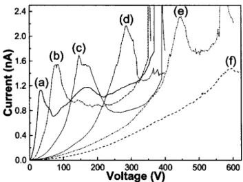
The TLM diode with contact spacing of 2.5m made on the BSO glass exhibits a completely insulating property with a negligible leakage current of only 5 pA at a bias of up to 350 V, which further decreases down to⬍1 pA as the contact spacing enlarges. After implanting, the BSO glass is no longer insulating owing to the generation of dense defects, as shown in Fig. 5. The leakage current of the BSO:Si⫹diode with 2.5m contact spacing is found to change from 0.25 to 600 pA at a bias of 50 V, which further increases up to 1.5 nA and turns to breakdown at a bias of 350 V or larger. The TLM measurements indicate that the total resistance of the BSO glass has reduced by four orders of magnitude after Si-ion implantation.23 At a bias of 20 V, the contact resis-tance, the sheet resistances, and the specific contact resistiv-ity of the BSO glass decrease from 1.8⫻1014⍀, 2.3 ⫻1015⍀/䊐, 7.7⫻108⍀ cm2 to 5.9⫻1010⍀, 8.6
⫻1012⍀/䊐, and 2.3⫻104⍀ cm2, respectively. In particular,
the as-implanted BSO:Si⫹diode exhibits an anomalous cur-rent overshooting phenomenon. For example, the leakage current of a BSO:Si⫹ diode with 1 m contact spacing greatly overshoots to 1.1 nA at a bias of 33 V, which subse-quently recovers back and overshoots again as the biased voltage increases up to 170 V. However, the secondary cur-rent overshooting behavior is relatively weak as compared to the first one. In comparison, the diode made on BSO glass only shows a linear current–voltage relationship before breakdown.23Such an anomalous carrier transport is known as the NDR phenomenon observed in a resonant tunneling diode made on conventional semiconductors. In general, the NDR results from the transfer electron effect observed in compound semiconductors, in which the hot electrons under FIG. 4. The normalized TRPL traces of as-implanted共solid line兲, 30 min
annealed 共dash-dot line兲, and 60 min annealed 共dotted line兲 BSO:Si⫹ samples.
FIG. 5. The current–voltage of MSM diodes with contact spacing of共a兲 1
m,共b兲 2.5m,共c兲 5m,共d兲 10m,共e兲 15m, and共f兲 20m fabricated on as-implanted BSO:Si⫹substrate.
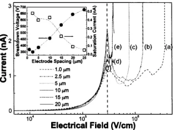
high electric field may exhibit higher kinetic energy to move from the central energy valley to the higher energy valley with heavier effective mass and lower drift velocity. Alterna-tively, the NDR can also be explained as the single or double barrier electron tunneling characteristic24 of the MSM diode made on all kinds of semiconductors. Some of the similar results observed in porous15 and amorphous16 Si semicon-ductors have been explained as the contribution of dense localized states which also induce the hopping conduction effect. As the contact spacing enlarges, the first overshooting peak upper-shifts to larger biased voltage associated with a higher current level, while the secondary overshooting peak gradually diminishes. If we further plot the leakage current of the as-implanted BSO:Si⫹diode as a function of electric field strength, the threshold electric field for the NDR of the as-implanted BSO:Si⫹sample is obtained as 2.9–3.5 kV/cm, as shown in Fig. 3共right兲. This value is very close to that of the diode made on bulk GaAs substrate, and is far smaller than a GaN-based device共80–150 kV/cm兲.25The breakdown voltage of the as-implanted BSO:Si⫹ diode increases from 350 to 680 V as the contact spacing enlarges from 1 to 25
m, as shown in the inset of Fig. 6. Before breakdown, the saturation current (Is) of the BSO:Si⫹ diode with 2.5 m
contact spacing is determined as 0.48 nA, which linearly decreases by approximately one order of magnitude as the contact spacing enlarges to 25m. In more details, the bar-rier height of the metal–BSO:Si⫹ junction can also be esti-mated if we consider the general formula of saturation cur-rent as
Is⫽AA*T2e⫺qB/kT,
where A and A* are the Richardson constants, T is the cir-cumstance temperature, andB is the barrier height in units
of eV. The barrier height for the as-implanted BSO:Si⫹diode is about 1.9 eV, which is in good agreement with that mea-sured by Kameda et al. using Fowler–Nordheim 共FN兲 theory.11This is the primary observation of the NDR effect in the planar MSM diode fabricated on as-implanted BSO:Si⫹
substrate, which strongly correlates with the dense defects induced by implantation rather than the Si nanocrystals.
After annealing for 30 min, the leakage current of the BSO:Si⫹diode is found to decrease by at least two orders of magnitude 共see Fig. 7兲. The contact resistance, sheet resis-tance, and specific contact resistivity of the annealed BSO:Si⫹ diode calculated from the TLM analysis also re-covers back to be 1.01⫻1014⍀, 1.46⫻1015⍀/䊐, and 3.93 ⫻108⍀ cm2, which are comparable with the values of the
same device made on BSO glass. The peak voltage for the weak current overshooting is found to upper-shift from 80 to 250 V. According to the double barrier tunneling theory, such a upper shift is mainly attributed to the increase in the barrier height of the metal–BSO:Si⫹ junction. To confirm, we have calculated the barrier height at the interface of metal and annealed BSO:Si⫹ from the diode saturation current, as shown in Fig. 8. Indeed, it is found that the barrier height of the metal–BSO:Si⫹ junction is also found to increase from 1.92 to 2.1 eV after a 30 min annealing process. As the annealing time increases up to 60 min or larger, the leakage current of BSO:Si⫹is reduced to be comparable with that of the BSO glass. The disappearance of the NDR effect in the annealed BSO:Si⫹ interprets that the Si-implanted defects FIG. 6. The current-field characteristics of MSM diodes with contact
spac-ing of共a兲 1m,共b兲 2.5m,共c兲 5m,共d兲 10m,共e兲 15m, and共f兲 20m fabricated on as-implanted BSO:Si⫹ substrate. The inset figure plots the breakdown voltage and saturation current of these diodes as a function of contact spacing.
FIG. 7. The leakage current of a metal–BSO:Si⫹–metal diode at different annealing times.
FIG. 8. The breakdown field strength共closed square兲 and the barrier height
共open square兲 of a metal–BSO:Si⫹junction at different annealing times. 7545 J. Appl. Phys., Vol. 94, No. 12, 15 December 2003 G.-R. Lin
electron tunneling mechanism in the as-implanted BSO:Si⫹. Although some Si nanocrystals might be grown under the low-temperature and long-term annealing process, which is less contributed to the electrical properties of the BSO:Si⫹ substrate based on our experimental observations.
IV. CONCLUSIONS
In conclusion, the effect of annealing time on the defect-induced anomalous electrical characteristics of low-temperature共500 °C兲 annealed silicon-implanted borosilicate glass (BSO:Si⫹) has been optically and electrically charac-terized. The weak and broadened XRD peaks reveal the in-significant formation process of sub-nm Si clusters even after long-term annealing, whereas the redshifted PL spectra con-firm the change in category and the decrease in density of irradiative defects in BSO:Si⫹. The carrier lifetimes of BSO:Si⫹ are found to lengthen from 1.7 to 2.8 ns after an-nealing at 500 °C for 60 min or longer. The density ratio of corresponding nonradiative defects (T1) in as-implanted, 30
min annealed, and 60 min annealed BSO:Si⫹ samples are 17.9:3:1.5. The TLM analysis reveals the dramatic changes in both the leakage current and the contact resistance of as-implanted BSO:Si⫹by at least three orders of magnitude. the diode made on as-implanted BSO:Si⫹exhibits strong current overshooting and rectified characteristics, however, which diminish after a long-term annealing process. The overshoot-ing voltage linearly increases as the diode contact spacovershoot-ing increases. The NDR phenomenon with a threshold electric field of 2.9–3.5 kV/cm and the associated double-barrier electron tunneling behavior are also observed. After implant-ing, the decrease in barrier height of the metal–BSO glass junction from 3.0 to 1.9 eV correlates well with the contri-bution of the deep-level defects with an activation energy of nearly 1 eV. After annealing for 30 min or longer, the leakage current and contact resistance of the metal–BSO:Si⫹ junc-tion recovers back to be comparable with those of the metal–
appreciated. The author thanks Chin-Chia Hsu for his effort in some of the experiments.
1S. Tiwari, F. Rana, H. Hanafi, A. Hartstein, E. Crabbe, and K. Chan, Appl. Phys. Lett. 68, 1377共1996兲.
2
K. D. Hirschman, L. Tsybeskov, S. D. Duttagupta, and P. M. Fauchet, Nature共London兲 384, 338 共1996兲.
3Y. Kanemitsu, Phys. Rep. 263, 1共1995兲.
4M. L. Brongersma, K. S. Min, E. Boer, T. Tambo, A. Polman, and H. A. Atwater, Mater. Res. Soc. Symp. Proc. 486, 275共1998兲.
5S. Hayashi, T. Nagareda, Y. Kanzawa, and K. Yamamoto, Jpn. J. Appl. Phys., Part 1 32, 3840共1993兲.
6L. Rebohle, J. Borany, R. A. Yankov, W. Skorupa, I. E. Tyschenko, H. Frob, and K. Leo, Appl. Phys. Lett. 71, 2809共1997兲.
7
G. H. Li, K. Ding, Y. Chen, H. X. Han, and Z. P. Wang, J. Appl. Phys. 88, 1439共2001兲.
8H. Z. Song, X. M. Bao, N. S. Li, and J. Y. Zhang, J. Appl. Phys. 82, 4028 共1997兲.
9
J. Gazecki, J. M. Kubica, M. Zamora, G. K. Reeves, C. M. Johnson, and M. C. Ridgway, Thin Solid Films 340, 233共1999兲.
10M. Y. Hao, H. Hwang, and J. C. Lee, Appl. Phys. Lett. 62, 1530共1993兲. 11E. Kameda, T. Matsuda, Y. Emura, and T. Ohzone, Solid-State Electron.
42, 2105共1998兲.
12
A. Kalnitsky, A. R. Boothroyd, and J. P. Ellul, Solid-State Electron. 33, 893共1990兲.
13R. D. Gould and M. G. Lopez, Thin Solid Films 343–344, 94共1999兲. 14M. C. Rossi, S. Salvatori, M. Burchielli, and G. Conte, Thin Solid Films
383, 267共2001兲.
15
A. I. Yakimov, N. P. Stepina, and A. V. Dvurechenskii, J. Phys.: Condens. Matter 6, 2583共1994兲.
16E. Lampin, C. Delerue, M. Lannoo, and G. Allan, Phys. Rev. B 58, 12044 共1998兲.
17
M. G. Lopez and R. D. Gould, Thin Solid Films 254, 291共1995兲. 18S.-J. Wang, J.-C. Lin, and H. Y. Tsai, Electron. Lett. 32, 1618共1996兲. 19M.-K. Lee, C.-H. Chu, Y.-C. Tseng, J.-M. Shyr, and C.-H. Kao, IEEE
Electron Device Lett. 21, 587共2000兲. 20
Q. Wan, N. L. Zhang, X. Y. Xie, T. H. Wang, and C. L. Lin, Appl. Surf. Sci. 191, 171共2002兲.
21G. Y. Xu, M. Liu, X. S. Wu, Y. L. He, and T. M. Wang, J. Phys.: Condens. Matter 11, 8594共1999兲.
22L. Tsybeskov et al., Europhys. Lett. 55, 552共2001兲. 23
G.-R. Lin, Jpn. J. Appl. Phys., Part 2 41, L1379共2002兲. 24O. Pinaud, J. Appl. Phys. 92, 1987共2002兲.
25E. Alekseev and D. Pavlidis, Solid-State Electron. 44, 941共2002兲.