Effect of surface pretreatment of submicron contact hole on selective tungsten
chemical vapor deposition
WenKuan Yeh, MaoChieh Chen, and MouShiung Lin
Citation: Journal of Vacuum Science & Technology B 14, 167 (1996); doi: 10.1116/1.589021 View online: http://dx.doi.org/10.1116/1.589021
View Table of Contents: http://scitation.aip.org/content/avs/journal/jvstb/14/1?ver=pdfcov
Published by the AVS: Science & Technology of Materials, Interfaces, and Processing
Articles you may be interested in
Effects of hydrogen surface pretreatment of silicon dioxide on the nucleation and surface roughness of polycrystalline silicon films prepared by rapid thermal chemical vapor deposition
Appl. Phys. Lett. 69, 485 (1996); 10.1063/1.118148
Selectivity loss during tungsten chemical vapor deposition: The role of tungsten pentafluoride
J. Vac. Sci. Technol. A 7, 621 (1989); 10.1116/1.575854
New insights on nucleation of tungsten on insulators during selective chemical vapor deposition
Appl. Phys. Lett. 50, 965 (1987); 10.1063/1.98000
Diffusion barrier properties of thin selective chemical vapor deposited tungsten films
J. Vac. Sci. Technol. B 4, 1369 (1986); 10.1116/1.583460
Barrier effect of selective chemical vapor deposited tungsten films
tungsten chemical vapor deposition
Wen-Kuan Yeh and Mao-Chieh ChenDepartment of Electronics Engineering, National Chiao Tung University and National Nano Device Laboratory, 1001 University Road, Hsinchu, Taiwan, Republic of China
Mou-Shiung Lin
Taiwan Semiconductor Manufacturing Company, Hsinchu, Taiwan, Republic of China ~Received 14 November 1994; accepted 11 November 1995!
The effects of various predeposition treatments of silicon substrates on selective tungsten chemical vapor deposition were investigated using the silane reduction process. The predeposition treatments include HF or buffered HF wet etch and/or NF3 plasma etch. The experimental results show remarkable differences in the initial nucleation of W and the smoothness of the W surface and the W/Si interface among the various treatments, as revealed by scanning electron microscope inspection and atomic force microscope analysis. Plasma etch leads to a rough W/Si interface while wet treatment with HF dip results in a fairly smooth interface. The experimental results show that better I – V characteristics for the W/n-Si Schottky contact can be obtained by the wet etch treatment prior to the W deposition. The reverse bias junction leakage for the wet etch pretreated W/p1n junction diode is smaller than that of the plasma pretreated diode. In addition, the substrate surface treatments were found to result in Si consumption of various degrees. © 1996 American Vacuum Society.
I. INTRODUCTION
Selective tungsten chemical vapor deposition~W-CVD! is one of the most attractive techniques for filling deep submi-cron contact holes and via holes for ultralarge scale inte-grated ~ULSI! applications. Selective W-CVD can be per-formed using the hydrogen ~H2! reduction1 or silane~SiH4! reduction2,3of tungsten hexafluoride~WF6!.
Selective W-CVD, using the H2 reduction process, can result in a high reactivity of WF6 toward the silicon sub-strate. Thus, it causes excessive Si consumption, encroach-ment at the Si/SiO2 interface, and worm hole formation in the contact regions.4,5These disadvantages do not occur dur-ing the silane reduction process.6 For both processes, the silicon displacement reaction takes place at the initial stage. Then, after a certain thickness of tungsten is formed, the silicon displacement reaction is self-limited by the tungsten film.7 It is expected and experimentally confirmed that the surface preparation has a profound effect on the Si consump-tion during W-CVD.
The common predeposition treatments of a Si substrate include HF etch, buffered HF~BHF! etch, and plasma etch. The Si~100! surface is isotropically and microscopically rough after being treated in dilute HF;8,9 it becomes even rougher when it is treated in BHF solution, due to~111! facet formation.10,11 The Si~100! surface after HF dip is mostly hydrogen passivated,12 while the fluorine coverage on the surface is only about 10% and can be further reduced to a few percent by deionized~DI! water rinse in 10 min.13 How-ever, this minority fluorine plays a significant role in enhanc-ing silicon surface oxidation.14During the DI water rinse, the Si–F species on the HF treated Si~100! surface rapidly inter-act with H2O to form Si–OH groups, and the condensation of Si–OH forms Si–O–Si bridges and SiO2.
15,16
The BHF
treated Si~100! surface was found to be almost purely hydro-gen terminated17 and extremely stable against reoxidation and contamination in air.18 After plasma etch in dilute NF3 gas, the Si surface was damaged and covered with fluorine species.19,20
The purpose of this article is to clarify the effects of vari-ous substrate surface treatments prior to conducting selective W-CVD using the silane reduction process on a contact hole patterned substrate. The predeposition treatments include wet etch with dilute HF or BHF and/or NF3 plasma etch. The experimental results show remarkable differences in the ini-tial nucleation stage of W as well as the smoothness of the W/Si interface among the various predeposition treatments.
II. EXPERIMENTAL DETAILS
The starting material was p-type^100& oriented Si wafers with 8 –12 V cm nominal resistivity. After RCA standard cleaning, the wafers were oxidized thermally to grow a 1500 Å thickness of SiO2, followed by deposition of 4500 Å of Borophosphosilicate glass ~BPSG!. A p1 junction implant was carried out by BF21implantation at 30 keV to a dose of 331015cm22followed by furnace annealing at 900 °C for 30 min in an N2ambient. Contact holes with sizes ranging from 0.6 to 1.2 mm were then defined on the wafers using the conventional photolithographic technique. Prior to selective W-CVD, the wafers were dipped in diluted HF~2%! or BHF solution, with a pH value of 4.5~7:1 mixture of 50 wt % HF in H2O and 40 wt % NH4F in H2O for 10–30 s, followed by a rinse in deionized water for 2 min. The wafers were then loaded into the load-locked cold wall W-CVD system within 5 min.
In this work, the predeposition plasma etch was con-ducted with the following conditions: rf power: 30–50 W; total gas pressure: 100 mTorr; NF3 flow rate: 12 sccm; and
N2flow rate: 72 sccm. After the plasma etch, the wafers were transferred by a robot arm from the plasma etch chamber to the deposition chamber without expose to the atmosphere. The base pressure of the CVD chamber is 1026Torr. Typical conditions for the W-CVD conducted in this work are as follows: substrate temperature: 280–320 °C; total gas pres-sure: 100 mTorr; WF6flow rate: 20–30 sccm; SiH4flow rate: 10–20 sccm; and H2carrier gas flow rate 1000 sccm. After the selective W-CVD, Al metalization was applied, followed by a 30 min sintering at 400 °C. The nucleation of W and the thickness of the tungsten film were determined by use of a scanning electron microscope~SEM!. The surface roughness of the W film was inspected by using an atomic force micro-scope~AFM!. The Fourier transform infrared ~FTIR! differ-ential spectrum was used to detect the formation of various bonds on the Si surface.
III. RESULTS
A. Surface microroughness after predeposition treatment
Figure 1 depicts the Si substrate surface after various
pre-FIG. 1. Silicon surface microroughness with and without predeposition treat-ments as determined by an AFM:~a! without pretreatment, ~b! with HF dip,
~c! with BHF dip, ~d! with HF dip followed by 30 W NF3plasma etch, and
~e! same as ~d! but with 50 W plasma etch.
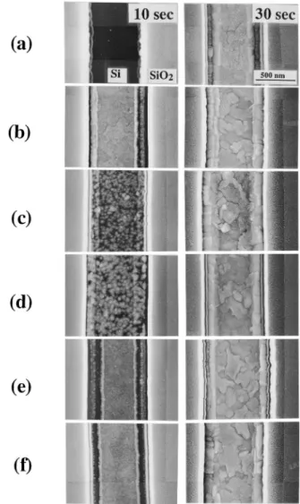
FIG. 2. The initial nucleation stage of 10~left! and 30 s ~right! selective W-CVD on Si surfaces inside submicron trench which had been treated with
~a! HF dip followed by DI water rinse, ~b! BHF dip followed by DI water
rinse,~c! HF dip followed by DI water rinse and subsequent NF3plasma
etch,~d! BHF dip followed by DI water rinse and subsequent NF3plasma
etch,~e! HF dip only, and ~f! BHF dip only.
FIG. 3. Thickness of tungsten film vs deposition time of W-CVD for various
predeposition surface treatments.
168 Yeh, Chen, and Lin: Surface pretreatment of submicron contact hole 168
deposition treatments, as determined by an AFM. It can be seen that the HF dipped surface@root-mean-square roughness rms50.203 nm, as shown in Fig. 1~b!# is much smoother than the BHF dipped surface @rms50.519 nm, as shown in Fig. 1~c!#. It should be noted that, in contrast with the HF-cleaned Si surface, whereon only the surface oxide was se-lectively removed, BHF attacks bulk silicon anisotropically.8 The use of buffered HF may be ill-advised in attempting to prepare atomically flat~100! surfaces, since ~111! facets de-velop upon the BHF etch. Increased surface roughness has been directly observed after BHF etch. A very smooth Si surface was [email protected] nm, as shown in Fig. 1~d!# after the 30 W plasma etch following the HF dip; however, the surface became very [email protected] nm, as shown in Fig. 1~e!# when the plasma power was raised from 30 to 50 W.
B. Initial nucleation stage of W-CVD
The SEM micrographs illustrated in Fig. 2 show the initial nucleation stage of 10 ~left! and 30 s ~right! selective W-CVD on the Si surface inside submicron trench which had received various predeposition treatments. The wet etch with dilute HF dip followed by DI water rinse resulted in a longer incubation time~or delayed nucleation of W! @Fig. 2~a!#. The incubation time was shortened when BHF was used instead FIG. 4. Surface roughness of tungsten film vs deposition time of W-CVD for
HF dipped substrates with and without additional NF3plasma etch.
FIG. 5. Cross section SEM micrographs showing W deposition in submicron contact hole for various substrate pretreatments:~a! HF dip, ~b! BHF dip, ~c! HF dip1plasma etch, and ~d! BHF dip1plasma etch. The deposition time was 180 s.
FIG. 6. Si consumption vs deposition time of W-CVD for two different predeposition treatments.
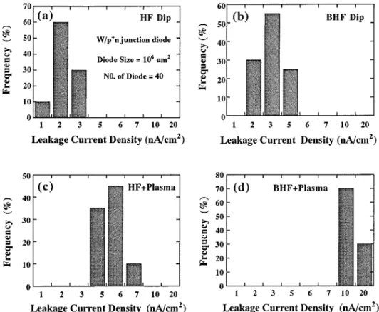
FIG. 7. The histograms showing the distribution of~a! reverse biased current measured at25 V, and ~b! forward ideality factor, for the W/n-Si Schottky diodes. The Si substrates were pretreated with four different wet and/or plasma etches.
of HF @Fig. 2~b!#. The NF3 plasma treatment further short-ened the incubation time@Figs. 2~c! and 2~d!#; the W nucle-ation sites can be clearly observed after 10 s W-CVD, and its morphology also looks different from those of the HF and BHF etched samples. The substrates with wet treatments, either HF or BHF, but without DI water rinse also resulted in very short incubation times @Figs. 2~e! and 2~f!#; it can be seen that the nucleation has rapidly developed into a smooth W film after 10 s of W-CVD. Figure 3 shows the thickness of tungsten film versus deposition time of W-CVD for various predeposition surface treatments. The incubation time is dif-ferent during the nucleation stage of W for the various pre-treatment cases, but the deposition rates of W-CVD eventu-ally became nearly equal~about 1800 Å/min!. Because of the different initial nucleation stages of W-CVD, the surface roughness of the W film is also different in the early period of CVD~e.g., in the first 60 s!. However, surface morpholo-gies for all samples did not show obvious differences after a prolonged deposition. Figure 4 shows the surface roughness of the W film versus deposition time of W-CVD for HF dipped substrates with and without additional NF3 plasma etch, as obtained by AFM.
C. Tungsten/silicon interface
Figure 5 shows the cross section SEM micrographs for the W-filled contact holes with 0.6 mm size. The HF and BHF etches resulted in a belt ring around the sidewall of the contact hole, due to the different etching rates between the
undoped SiO2 and BPSG films. It can also be seen that wet etch with HF dip resulted in a very smooth W/Si interface @Fig. 5~a!#, while the plasma etch led to a rough W/Si inter-face@Figs. 5~c! and 5~d!#. The BHF etch resulted in slightly more consumption of Si compared to the HF etch, because NH4F will attack the bulk Si anisotropically@Fig. 5~b!#. The subsequent plasma etch will cause further Si consumption depending on the plasma power; higher power resulted in increased Si consumption. The Si consumption was indepen-dent of the deposition time of W-CVD, as revealed in Fig. 6. The Si displacement process takes place only at the begin-ning of W-CVD, and the thickness of Si consumption re-mained constant during the entire deposition time of W-CVD at temperatures below 400 °C.21
D.I – V characteristics
The current–voltage characteristics were measured on the W/n-Si Schottky contact diodes and W/p1n junction diodes, which were fabricated by selective W-CVD on the variously pretreated Si substrates with defined diode areas of 1000 31000mm2. At least 40 randomly chosen diodes were mea-sured in each case. Figure 7 illustrates the histograms show-ing the distribution of the reverse biased current and forward ideality factor for the W/n-Si Schottky contact diodes. The Schottky diodes with wet treatment prior to the W deposition revealed better I – V characteristics than those with additional plasma treatment. This result is consistent with the SEM ob-servation, as shown in Fig. 5, that the predeposition plasma FIG. 8. The histograms showing the distribution of reverse leakage current density measured at25 V for the W/p1n junction diodes. The Si substrates were
pretreated with four different wet and/or plasma etches.
170 Yeh, Chen, and Lin: Surface pretreatment of submicron contact hole 170
treatment resulted in a fairly rough W/Si interface after the W deposition. It also shows that the Schottky diodes, made with wet treatment, have a scattered distribution of reverse current and ideality factor.
Figure 8 illustrates the histograms showing the distribu-tion of the reverse leakage current density measured at25 V for the W/p1n junction diodes with various predeposition substrate treatments. The average reverse leakage current density for the junction diodes with HF treatment is 2 nA/cm2. The reverse leakages for the junction diodes with wet treatment and an additional plasma treatment were found to be about three times larger than those of the diodes which did not receive the plasma etch. The plasma treatment tended to result in more Si consumption and a rough W/Si interface after the selective W-CVD. This is presumably the main rea-son for the increased reverse leakage for the shallow junction diodes.
IV. DISCUSSION
In general, only two chemistries have been seriously stud-ied with respect to selective tungsten deposition: H2/WF6 ~hydrogen reduction process! and SiH4/WF6 ~silane reduc-tion process!. In this work, the SiH4 reduction process was used in order to avoid the HF by-product of the H2reduction process which would cause undesirable excessive Si con-sumption. Nonetheless, in both processes, the first reaction that occurs between Si and WF6is the so-called Si displace-ment reaction.
During the Si displacement reaction, WF6first dissociates on the Si surface forming WFx(x,6) adsorbed on the
sur-face, and then further reduces to W. At the same time, Si is converted into SiFx(x>1) and further changes to SiF4. The overall process can be expressed as7
2WF613Si→2W13SiF4 ~T,400 °C!.
The Si surface must be fluorided or hydrided first so as to adsorb the WF6 molecule. The HF-cleaned Si surface is mostly hydrogen passivated. The hydrogen terminated sur-face is surprisingly stable in the air towards reoxidation. The FTIR spectrum shown in Fig. 9~a! confirms the existance of the Si–H bond~2080–2160 cm21!. In fact, small amounts of fluorine also existed on the HF treated Si surface, and the fluorine-terminated surface was oxidized rapidly in water.22 The fluorine-terminated surfaces are much more reactive with water than the hydrogen-terminated surfaces. When the HF dipped wafer is rinsed by deionized water, the flourine-terminated surface~Si–F bond! will be converted to Si–OH species. The FTIR spectrum shown in Fig. 9~b! shows that the HF-cleaned Si surface produced Si–OH bond ~3200– 3700 cm21! after DI water rinse for 2 min, which is consis-tent with those reported in the literature.23 Condensation of Si–OH forms Si–O–Si bridges which is the prestage of SiOx.
15,16
The native oxide ~SiOx! will interfere with the
incubation of tungsten and increase the nucleation time of W-CVD@Fig. 2~a!#.
In contrast to the HF-cleaned Si substrate, the Si surface after BHF dip was found to be almost purely hydrogen
ter-minated which is extremely stable against reoxidation and contamination in the air. The existance of the Si–H bond is confirmed, as shown in Fig. 10~a!. The BHF-cleaned surface, which does not exhibit surface fluorine, ought to be stable during the subsequent water rinse.14Figure 10~b! shows that the BHF-cleaned and DI water rinsed surface did not reveal any obvious Si–OH peak. Therefore, the incubation time of W-CVD on the BHF-cleaned Si surface followed by DI wa-ter rinse @Fig. 2~b!# is shorter than that on the HF-cleaned and DI water rinsed Si surface@Fig. 2~a!#. If the wet etching of HF or BHF is not followed by the DI water rinse, the Si–H and Si–F bonds produced on the HF-cleaned Si sur-face and the Si–H bonds produced on the BHF-cleaned Si surface would attract the WF6 molecules to the Si surface and enhance the nucleation of W film @Figs. 2~e! and 2~f!#.
For the plasma etched substrate, the NF3 plasma breaks the Si–Si bonds on the Si surface and produces a large amount of surface damage.19,24This surface damage, which has lower potential energy, will easily attract the WF6species to react with Si and further proceed with the nucleation of W islands. The W islands will cause nonuniform Si consump-tion leading to rough W/Si interface. Although both the Si–H and Si–F dangling bonds exist on the HF-cleaned Si sub-strate, the WF6molecules are first attracted to the Si–F bond
FIG. 9. FTIR differential spectrum for the Si surface after~a! HF dip only and~b! HF dip followed by deionized water rinse for 2 min.
which has a lower potential energy25 and proceed with the displacement reaction. Silicon reduces the WF6 molecules, leading to the deposition of a W film. The tungsten surface, either by retaining some of the fluorine or adsorbing more WF6species, is highly fluorinated; thus, SiH4reacts with this surface to form W, leaving SiF4and H2on the surface.26On the other hand, the WF6 molecules need more energy to break the Si–H bond that exists on the Si surface. When the Si–H bond is broken, the WF6species will react with the H atom and reproduce the HF species which will cause Si con-sumption to some extent, like the H2 reduction process. In all, during the initial nucleation stage of W film, the Si dis-placement process which proceeds on the Si–F bond, and the H2reduction process which proceeds on the Si–H bond, will occur simultaneously until the Si surface is entirely covered with a W film. After that, the W film deposition is completely taken over by the silane reduction process. Figure 11 shows the secondary ion mass spectroscopy ~SIMS! depth profiles of the CVD W films deposited on the HF dipped and DI water rinsed Si substrate with and without a subsequent NF3 plasma etch. The deposition time of the W-CVD was 20 s. A very high concentration of fluorine is observed in the W film deposited on the plasma etched substrate@Fig. 11~a!#. On the
other hand, a relatively thin W film was deposited on the HF-cleaned and DI water rinsed Si substrate, and the film contained a very low concentration of fluorine @Fig. 11~b!#.
V. SUMMARY
The Si substrate surface condition imposes great influence on the behavior of W-CVD. The experimental results indi-cate remarkable differences in the initial nucleation stage of W as well as the smoothness of W/Si interface among the various predeposition treatments of substrate surfaces. Both Si–H and Si–F bonds were produced on the HF-cleaned Si substrate surfaces, while only Si–H bonds were produced on the BHF-cleaned surfaces; either the Si–H or the Si–F bond-ing enhanced the W nucleation. If the HF-dipped wafer is followed by DI water rinse, the surface will produce a large number of Si–OH species which will retard the nucleation of W. On the other hand, if the BHF-dipped wafer is followed by DI water rinse, the surface remained to be hydrogen ter-minated and the nucleation of W still can be enhanced. With additional NF3 plasma etching following the wet treatment, the large amount of surface damage produced on the Si sub-strate will attract the WF6 molecules to react with Si and eventually lead to the nucleation of W islands. Thus, it was found that the wet etch of the Si substrate using dilute HF resulted in an increased incubation time and a very smooth W/Si interface. The plasma etch resulted in a shortened in-FIG. 10. FTIR differential spectrum for the Si surface after~a! BHF dip only
and~b! BHF dip followed by deionized water rinse for 2 min.
FIG. 11. SIMS depth profiles of the CVD W films deposited on Si substrates which was~a! HF dipped followed by DI water rinse and then NF3plasma
etched, and~b! HF dipped followed by DI water rinse. The deposition time of the W-CVD was 20 s.
172 Yeh, Chen, and Lin: Surface pretreatment of submicron contact hole 172
cubation time and a rough interface. In addition, better I – V characteristics were found for the W/n-Si Schottky diodes and the W/p1n junction diodes with the Si substrates wet etched in dilute HF prior to the selective W-CVD rather than etched in NF3plasma.
ACKNOWLEDGMENT
This work was supported by the National Science Council ~ROC! under Contract No. NSC84-2622-E009-007-1.
1C. M. McConica and K. Krishnamani, J. Electrochem. Soc. 132, 2542
~1986!.
2R. F. Foster, S. Tseng, L. Lane, and K. Y. Ahn, Tungsten Workshop III
~Materials Research Society, Pittsburgh, 1988!, p. 69.
3Y. Kusumoto, K. Takakuwa, H. Hashinokuchi, T. Ikuta, and I. Nakayama, Tungsten Workshop III~Materials Research Society, Pittsburgh, 1987!,
p. 103.
4
W. T. Stacy, E. K. Broadbent, and M. H. Norcott, J. Electrochem. Soc. 132, 444~1985!.
5R. A. Levy, M. L. Green, P. K. Gallagher, and Y. S. Ali, J. Electrochem.
Soc. 133, 1905~1986!.
6R. S. Rosler, J. Mendonca, and M. J. Rice, Jr., J. Vac. Sci. Technol. B 6,
1721~1988!.
7E. K. Broadbent and C. L. Ramiller, J. Electrochem. Soc. 131, 1427
~1984!.
8G. J. Pietsch, U. Kohler, and M. Henzler, J. Appl. Phys. 73, 4797~1993!.
9Y. J. Chabal, G. S. Higashi, and K. Raghavachari, J. Vac. Sci. Technol.
A 7, 2104~1989!.
10D. Graf, M. Brohl, S. Bauer-Mayer, A. Ehlert, P. Wagner, and A. Schnegg,
Mater. Res. Soc. Symp. Proc. 315, 23~1993!.
11
Y. J. Chabal, Mater. Res. Soc. Symp. Proc. 259, 349~1992!.
12
M. Grundner and H. Jacob, Appl. Phys. A 39, 73~1986!.
13T. Sunada, T. Yasaka, M. Takakura, T. Sugiyama, and M. Hirose, Jpn. J.
Appl. Phys. 29, L2408~1990!.
14R. A. Haring and M. Liehr, J. Vac. Sci. Technol. A 10, 802~1992!. 15
D. Graf, M. Grunder, and R. Schulz, J. Vac. Sci. Technol. A 7, 808~1989!.
16
D. Graf, M. Grunder, and R. Schulz, J. Appl. Phys. 68, 5155~1990!.
17P. Dumas and Y. J. Chabal, J. Vac. Sci. Technol. A 10, 2160~1992!. 18M. Morita, T. Ohmi, E. Hasegawa, M. Kawakami, and M. Ohwada, J.
Appl. Phys. 68, 1272~1990!.
19W. Kern, Handbook of Semiconductor Wafer Cleaning Technology
~Noyes, Park Road, NJ, 1993!, pp. 224–225.
20G. Bruno, P. Capezzuto, G. Cicala, and P. Manodoro, J. Vac. Sci. Technol.
A 12, 690~1994!.
21M. L. Yu, B. N. Eldridge, and R. V. Joshi, Tungsten Workshop III
~Mate-rials Research Society, Pittsburgh, 1988!, p. 75.
22
M. Hirose, T. Yasakura, and S. Miazaki, Solid State Technol. 12, 43
~1991!.
23T. Takahagi, I. Nagai, A. Ishitani, and H. Kuroda., J. Appl. Phys. 64, 3516
~1988!.
24V. M. Donnelly, D. L. Flamm, W. C. Dontremont-Smith, and D. J.
Wer-der, J. Appl. Phys. 55, 242~1984!.
25
C. G. Van De Walle, Mater. Res. Soc. Symp. Proc. 259, 375~1992!.