Generalized Hot-Carrier Degradation and
Its Mechanism in Poly-Si TFTs
Under DC/AC Operations
Ya-Hsiang Tai, Shih-Che Huang, Po-Ting Chen, and Chih-Jung Lin
Abstract—In the previous report, we had reported the mecha-nism for the degradation of poly-Si TFTs under OFF region gate ac operation with the source and drain electrodes grounded. In this paper, the study is extended to the degradation of the devices under various ac and dc operation conditions. It is discovered that, though these stress conditions are different, the corresponding degradation behaviors in their I–V and C –V curves all resemble the degradation behavior of the device under dc hot-carrier stress. Two important factors, namely, the electric field across the junc-tion and the number of carriers flowing through the juncjunc-tion, are taken into discussion in this paper and comparison of these stress conditions. It is then categorized that these operation conditions can be described as the “generalized hot-carrier effect,” since the degradation is found to occur near the junctions by the energized carriers, just as that under dc hot-carrier stress. The qualitative comparison of the electric field and carrier flow through the junction for the four stress conditions as well as the difference in the degradation mechanism between MOSFETSand poly-Si TFTs are also provided.
Index Terms—AC stress, dynamic stress, poly-Si TFTs, reliability.
I. INTRODUCTION
P
oly-Si TFTs, which have the similar structures as the MOSFETS, are now under extensive studies for the appli-cations in display system. The high device mobility of these de-vices enables the possibility to form both the in-pixel switches and integrated circuits with the poly-Si technology, which may greatly reduce the process complexity and fabrication cost. [1] The high device mobility also enables some special value-added functions to be integrated into the display panel. [2], [3] Devices in such applications would be dynamically operated and the operation conditions could be very different from those in the pixel. Though recently, several kinds of products formed with poly-Si technology have hit the market, the degradation mechanisms of the devices under dynamic operation are stillManuscript received July 11, 2010; revised September 18, 2010 and December 4, 2010; accepted December 23, 2010. Date of publication January 6, 2011; date of current version March 9, 2011. This work has been sponsored by the National Science Council, Republic of China (NSC98-2218-E-009-004-).
Y.-H. Tai, P.-T. Chen and C.-J. Lin are with the Department of Photonics & Display Institute, National Chiao Tung University, Hsinchu 30010, Taiwan (e-mail: [email protected]).
S.-C. Huang is with the Department of Photonics & Institute of Electro-Optical Engineering, National Chiao Tung University, Hsinchu 30010, Taiwan. Color versions of one or more of the figures in this paper are available online at http://ieeexplore.ieee.org.
Digital Object Identifier 10.1109/TDMR.2010.2104152
TABLE I
STRESSCONDITIONS AND THECORRESPONDINGDENOTATIONS
not so clear. Y. Uraoka previously reported that the degradation behavior of the devices under gate ac operation between itsON andOFFregions with source/drain grounded can be attributed to the swept carriers as the device is about to be turned off. [4], [5] In addition to the gate acON/OFFregion toggling, the device could also be operated some time in theOFFregion alone. How-ever, there are few papers on such reliability behavior. We had reported the degradation behavior for the device operated in the OFFregion with source/drain grounded and it had been experi-mentally proposed that the degraded behavior can be attributed to the source and drain junction degradation during stress. [6] Nevertheless, the detailed degradation mechanism about how the junction would degrade under such operation is still not clear. In this paper, the explicit degradation mechanism would be explored, starting with the comparison of the device behavior under gate acOFFregion operation and the dc hot-carrier stress. The carrier source and the electrical field distribution during stress would be discussed and other stress conditions would be performed and compared. The idea of the “generalized” degradation model for the various stress conditions would be provided. The four stress conditions are summarized in Table I and named as “condition #1” to “condition #4” in the following discussion in order to make the manuscript more legible.
II. EXPERIMENTS
Top-gate poly-Si TFTs with width/length of 20 μm/5 μm were fabricated using low-temperature process. First, the buffer oxide and a-Si:H films with thickness of 50 nm were deposited on glass substrates with PECVD. The samples were then placed 1530-4388/$26.00 © 2011 IEEE
in the oven for dehydrogenation. The XeCl excimer laser of wavelength 308 nm and energy density of 400 mJ/cm2 was then applied. The laser scanned the a-Si:H film with beam width of 4 mm and 98% overlap to recrystallize the a-Si:H film to poly-Si. After poly-Si active area definition, 50-nm SiO2
and 25-nm SiNX were deposited with PECVD as the gate insulator. Next, the TFT gate was formed by metal sputtering and then defined by photolithography. The lightly doped drain (LDD) and the n+ source/drain doping were formed by PH3
implantation with dosage 2× 1013 cm−2 and 2× 1015 cm−2 of PH3, respectively. The LDD implantation was self-aligned
and the n+ regions were defined using a separate mask. Then,
the interlayer of SiNX was deposited. Subsequently, dopants were activated via rapid thermal annealing while the poly-Si film was hydrogenated simultaneously. Finally, the contact hole formation and metallization were performed to complete the fabrication work. The typical value of the threshold voltage for the fresh devices is 1.63 V.
Rectangular pulses applied to the TFTs are generated with an Agilent 41501B pulse generator and the dc stress is performed by using an Agilent 4156A precision semiconductor parameter analyzer. The capacitance–voltage (C–V ) curves were mea-sured with an Agilent E4980A precision LCR Meter.
III. RESULT ANDDISCUSSION
A. Gate AC Stress in the OFF Region
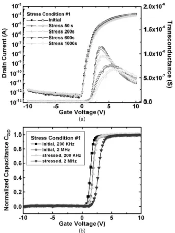
Fig. 1(a) shows the transfer characteristics of poly-Si TFTs before and after gate ac stress in the OFF region. The stress condition is that the ac signal toggling between 0 V and−20 V at 500 kHz with 50% duty cycle is applied to the gate electrode while the source and drain electrodes are grounded during stress. During stress, there should be no induced carriers formed and the degradation should be negligible since the device is kept in theOFFregion. However, it would be surprising to find that the device exhibits severe degradation after stress, particularly for the ON current and the transconductance. Fig. 1(b) gives the gate-to-drain capacitance–voltage (C–V ) behavior CGDfor
the device before and after 200-s gate ac stress. The CGD
be-havior is measured with the source electrode floated. The stress condition is the same as Fig. 1(a). The normalized capacitance is the ratio of the measured capacitance to the gate insulator capacitance of the TFT. As for its C–V behavior, the effect of such stress is that for the low measuring frequency, the curve for the stressed device shows slight shift, but for the high measuring frequency, the curve for the stressed device shows both shift and distortion. In other words, the effect of such degradation on the device’s C–V behavior is frequency-dependent. This behavior somehow indicates that the degradation can be attributed to the states generated during stress rather than the trap charges, since trap charges would not respond to different measuring frequen-cies or result in the dispersion behavior in the C–V curves [7]. Such degradation behavior would be worthy of discussion since for the similar device structure, namely, MOSFETS, there is no such degradation behavior reported.
The difference between MOSFETS and poly-Si TFTs one may first think of is the difference between their structures.
Fig. 1. (a) The current transfer behavior at VD= 5 V and (b) the normalized gate-to-drain capacitance CGDfor the poly-Si TFT before and after 200-s gate ac stress in theOFFregion.
There is a substrate electrode in MOSFETSand the carriers may be discharged through the substrate electrode during the OFF state toggling operation. The existence of the substrate electrode would also greatly affect the electric field near the substrate since in most operation conditions, it is grounded. As in the case of poly-Si TFTs, the lack of substrate electrode leaves the electric field near the substrate floated and also makes it rather difficult to analyze the behavior in the channel and substrate when the device is in the OFFregion. One way to analyze the electric field distribution is by utilizing the TCAD simulation tools. However, the present programs avail-able could only simulate the field distribution in dc operation, and thus it may not help to solve the degradation behavior under such ac operation.
Regarding such anomalous degradation behavior, we had proposed a device circuit model composed of the gate insulator capacitance, the channel resistance, and the source/drain junc-tion to analyze what could happen during stress. By examining the voltage distribution across each element during stress, it was inferred that during the gate ac stress in the OFF region, the largely reverse-biased junction could lead to the degradation. The gated p-i-n device was then specially adopted to verify our inference. [6] However, in that report, we had not discussed how the largely reverse-biased junction could lead to the changes in the mobility and the C–V behavior for the stressed device. In the following discussion, several other stress conditions would be performed to help discover the explicit degradation mechanism. The first one to be discussed and compared is the
Fig. 2. (a) The current transfer behavior at VD= 5 V and (b) the normalized gate-to-drain capacitance CGDfor the poly-Si TFT before and after 200-s dc hot-carrier stress.
hot-carrier effect. Its features on poly-Si TFTs are the obvious mobility andONcurrent degradation while the subthreshold re-gion remains almost unchanged, which resembles the behavior in Fig. 1(a). It would be a good start since there are already reports on the behaviors of poly-Si TFTs under hot-carrier stress conditions. [8]
B. DC Hot-Carrier Effect
Hot-carrier effect, as many works have reported, is closely related to the distribution of the lateral electric field in the channel and therefore is in relation with the applied drain voltage VDS and gate voltage VGS. As referred to the studies
of hot-carrier effect on MOSFETS, for the n-type devices, the high electric field near the drain region would accelerate the carriers and these carriers may attain enough energy to break the Si bonds as well as the Si/SiO2 interface, resulting
in the increase of states. The increase in states would affect the conduction for the gate voltage larger than the threshold voltage
VTHand then degrade the device mobility [9]. For MOSFETS,
when the large VDS is applied, the degradation mechanism is
different for different applied VGS. Generally, the degradation
is worst when VGS is around VDS/2. [10], [11] Unlike in
MOSFETS, hot-carrier effect in TFTs becomes most severe as
VGS is just above VTH and VDSis large [8]. Since the active
region in the poly-Si TFTs contains many grain boundaries, the effect of hot-carrier stress may be more complicated than that in MOSFETS. Fig. 2(a) shows the current transfer characteristics for the poly-Si TFTs before and after hot-carrier stress. The
stress condition is that the stress gate voltage VGSis 3 V and the
drain voltage VDSis 20 V. Referring to the previous report, the
hot-carrier effect causes the increase of the tail states in the band gap of the poly-Si film [10]. Fig. 2(b) gives the normalized CGD
behavior for the device before and after 200-s stress. It can be observed that the C–V behaviors for the stressed device show slight shift for the lower measuring frequency and the apparent shift and distortion for the higher measuring frequency. A more detailed discussion was reported in our other publication. [13] However, comparing the I–V and the C–V behaviors of the gate ac stress in the OFF region and the dc hot-carrier stress, respectively denoted as “stress condition #1” and “stress condition 2” hereafter, these two stress conditions result in the very similar degradation behaviors. The difference between them is just the degree of the degradation. Stress condition #2 leads to much worse degradation than stress condition #1.
The explicit degradation mechanism for the stress condi-tion #1 is still not clear yet, but there are already several reports on the stress condition #2. The mechanism of hot-carrier stress is that the large electrical field across the drain-side junction and the channel carriers under this large field could achieve high energy and interact with lattice. Thus, the two key components, the electric field over the junction and the carriers under such field, can be used in analyzing the degradation mechanism of stress condition #1. Though in the previous paper, the degradation is found to be resulted from the electrical field over the junctions, there should be no in-duced carriers since during stress, the applied VGS is kept all
below its VTH. One possible carrier source could be the junction
leakage current, but it would be rather difficult to probe the current during stress. Also, the current level of such leakage current is much smaller than that under the dc hot- carrier stress. Still an alternative method can be adopted, that is, by changing the experiment to dc stress with large VDbiased in the OFFstate, which would be studied in the following section and denoted as stress condition #3. The purpose of such study is that under large VDin theOFFregion, the drain-side junction would be subject to the large electric field and at the same time, there would be a small dc leakage current flowing across the junction. The comparison between the degradation behavior under stress condition #3 and the previous two degradation behaviors would help us find the explicit degradation mechanism for the different stress conditions.
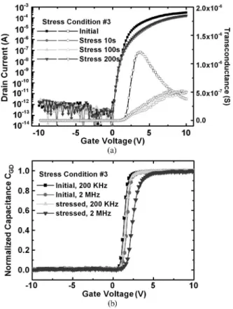
C. DC OFF Region Drain-Biased Stress
Fig. 3(a) shows the transfer characteristics of the n-type poly-Si TFT before and after stress condition #3 and Fig. 3(b) shows the normalized CGDcurves before and after 200-s stress.
The stress condition is that the stress VGSis−5 V and VDSis
20 V. The stress condition is chosen to make the large electric field occur at the drain junction but at the source side, the voltage difference is not large such that the degradation near the source side is small and thus simplifies the analysis. The I–V and C–V behaviors for the device after stress condition #3 are just very similar to those under the previous two kinds of stress conditions, as given in Figs. 1 and 2. However, in the case of stress condition #3, there is a large electric field over the drain
Fig. 3. (a) The current transfer behavior at VD= 5 V and (b) the normalized gate-to-drain capacitance CGDfor the poly-Si TFT before and after 200-second dcOFFregion drain-biased stress.
junction but the only possible current source is the dc junction leakage. It could be surprising to find the degradation behavior is obvious and similar to the previous two stress conditions. The difference between them is just the degree of degradation.
The similarities between the degradation behaviors could enlighten us to find the explicit degradation mechanism. Under theOFFregion drain dc stress, namely, stress condition #3, the depletion region near the drain side will be large and forms the large electric field near the drain-side junction. The gate voltage is purposely kept below the device’s VTH, making the
device stay in the OFF region. In this case, only the junction leakage current could be present and thus it can be inferred that the degradation can be attributed to the effect of the leakage current under the large drain-side electric field. As compared to the dc hot-carrier stress, namely, stress condition #2, though the current level is different, device under drain dc stress also exhibits the degradation behaviors similar to the other two stress conditions. Compare the above three degradation behaviors, it may thus inferred that once the large electric field is applied across the junction, the device would then suffer the degradation similar to the hot-carrier effect, no matter the carrier source is theONcurrent, the dc junction leakage current or the current through the junction when the gate ac signal below its VTH is applied. The difference between the effects
of stress is just the degree of degradation.
Still, it would be of interest to compare the aforementioned degradation behaviors with another dynamic operation, namely, the gate ac signal toggling between the ON andOFF regions. It was previously reported that such degradation behavior can
Fig. 4. (a) The current transfer behavior at VD= 5 V and (b) the normalized gate-to-drain capacitance CGDfor the poly-Si TFT before and after 200-s gate ac stress.
be categorized as another kind of hot-carrier stress, which may be relevant to our discussion. [5] The study and comparison of this behavior would be helpful to clarify the degradation mechanism.
D. Gate AC Stress Toggling Between ON/OFF Region
Fig. 4(a) gives the ID–VG curves before and after gate ac stress toggling between the ON/OFFregions, which would be denoted as stress condition #4 in the following discussion. The stress condition is that the stress gate voltage toggling between
−15 V and 15 V while the source and drain electrodes are
grounded. The stress gate voltage is of 500 kHz with 50% duty ratio. Fig. 4(b) gives the C–V behaviors for the device before and after 200-s stress. All these degradation behaviors are just similar to the behaviors under previous three stress conditions.
It is previously reported that the degradation of the device under stress condition #4 can be attributed to the induced carriers being swept to the source and drain regions as the gate voltage is switched fromONtoOFFregion. [5] Since the falling time of the gate pulse is around several hundred nanoseconds, the lateral electric field would be large and thus electrons could attain high energy and become hot carriers. These electrons could interact with the lattice and in turn lead to the generation of defect states. Such gate ac stress condition satisfies the aforementioned two factors for the hot-carrier effect, namely, the electric field over the junction and the carriers flow through the junction. In this case, the electric field over the junction
Fig. 5. Two components for forming the generalized hot-carrier stress effect.
Fig. 6. Mobility degradation ratio for the four stress conditions.
becomes large as the gate signal is switched fromON toOFF and the carriers are the induced channel carriers.
E. Discussions
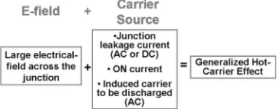
Comparing all four stress conditions, it can be summarized that once the electric field is across the junction, the device can then suffer the hot-carrier-like degradation. The carrier source can be the dc ON current, the dc OFF current, the induced carriers to be swept to the source and drain region, and the leakage current through the junction when the gate ac signal in theOFFregion is applied. Thus, all these four stress conditions can be categorized as the “generalized hot-carrier effect,” as illustrated in Fig. 5. Though the current level and the voltage drop across the junction may be different from each other, it can be observed that the device will all suffer the similar degradation. The difference is just the degree of the degradation. Fig. 6 gives the mobility degradation ratio for the device under the four aforementioned stress conditions. It can be observed that the degradation behaviors under the four stress conditions all exhibit the similar power-law time dependence. The mobility degradation can be fitted with the power-law Atn, where A and n are fitting parameters. The fitting curves as well as the parameter n are also shown in the figures and it can be observed that the fitting curves can fit the degradation trend very well. This behavior resembles the degradation behavior of MOSFETS under dc hot-carrier effect. [14] Refer to the figure, it can be observed that the dc hot-carrier stress results in the most severe degradation, and theOFFregion gate ac stress leads to the smallest degradation. A guessed table of the electric field magnitude and the carrier number as well as the degree of degradation for all four stress conditions is given in Table II. As for the electric field near the junction, dc operation should lead to a larger value of electric field and among stress condition #2
and #3, because in stress condition #3, the device is in theOFF state, the voltage difference VGD would mainly occur at the
drain junction and thus it poses the largest electric field near the junction. And for ac stress, because in stress condition #1, the device is kept inOFFstate, the total 20 V voltage difference would almost be at the junctions. For stress condition #4, as the device is switched from +15 V to around its VTH, which is
around 1.6 V, the channel can still be easily discharged since it is still in ON region. As the gate voltage is switched to a more negative voltage, namely, −15 V, the device is in the OFF state and the voltage difference VGD would be mainly
occurred at the junction. Though during the transient moment, the electric field distribution is hard to calculate, the value of the electric field near the junction should be less than that in stress condition #1.
As for the carrier number during stress, the number of the carrier should be the largest in stress condition #2 since this operation condition is in the ONregion. Another one that par-tially operated in theONregion is stress condition #4. Though the applied gate voltage is larger than stress condition #2, many of the induced carriers may just be discharged during the period the gate voltage switching from +15 V to its VTH.
Stress conditions #1 and #3 are in theOFFregion so the current level would be relatively small and the leakage current in stress condition #3 would be larger than that in condition #1 since its electric field is larger. Considering the electric field and the carrier number for each stress condition and comparing it with the degradation in mobility, it is discovered that the degradation itself is more like a synergy effect containing the electric field and carrier number, and not simply depends on one of the two components. It can be found that stress condition #2, namely, the hot-carrier stress, leads to the worst degradation because of its high electric field and large number of channel carrier. Stress condition #3, namely, theOFFregion drain dc stress, results in the worse degradation behavior because of the largest electric field, though its current is relatively small. Stress condition #1 and #4 are of relatively small electric field and carrier number, and since stress condition #4 induces more carriers, the degra-dation is more serious. In brief, by considering the electric field at the junction and the carrier number flow through the junction during stress, the degree of degradation can be roughly ranked and compared.
So far, it is clarified that how these generalized hot-carrier operation conditions would lead to different degree of degra-dation. And the degradation is found to be closely related to the electric field over the junction and carrier number. This finding helps to elucidate that the degradation mechanism is the carriers get accelerated by the large electric field near the junction and then interact with the lattice. Still there is one question left: Why such degradation behavior is not observed in the MOSFETS. There may be several reasons to this question. First, the operation voltage for poly-Si TFTs is usually above 10 V in the display applications, which is around two to three times larger than that for MOSFETSand thus the degradation would be much worse. Also, the poor crystallinity of the poly-Si film may be a critical factor, since it was reported that in poly-Si TFTs, the hot carrier effect is closely related to the be-havior and number of the grain in the poly-Si film. [15] Another
TABLE II
GUESSEDTABLE FOR THEELECTRICFIELD AT THEJUNCTIONS AND THECARRIERNUMBERALONG
WITH THEMOBILITYDEGRADATION FOREACHSTRESSCONDITION
main reason is the difference in the leakage behavior between the MOSFETSand poly-Si TFTs. The main leakage current sources of MOSFETS are P-Nreverse bias current (between the drain side and well junction), the subthreshold conduction (along with the drain-induced barrier lowering effect), the gate-induced drain leakage, and the punch-through effect, which, respectively, corresponds to different places inside or near the device. [16] On the other hand, the main leakage source of poly-Si TFT is in the drain-side depletion region. As the drain junction is largely reverse-biased, three conduction mecha-nisms associated with traps, namely, the tunneling, thermionic emission, and thermionic field emission, may happen. [17] Because poly-Si film is composed of small grains, in the drain-side depletion, a large number of traps would exist in the band gap, which in turn enhances the leakage behavior. This is very different from MOSFETSand thus the aforementioned degradation behavior is not observed in MOSFETS. This could also somehow explains why for poly-Si TFTs, once the large electric field is at the junction, the aforementioned generalized hot-carrier effect could occur.
As the advanced display applications adopting poly-Si TFT technology have hit the market, some more emerging appli-cations, such as smart phone and touch panel with multiple value-added functions, require much more understanding of the reliability behavior and evaluation of poly-Si TFTs under various operation conditions. Since in these applications, the TFTs are expected to work as the in-pixel switches as well as the circuit elements in various kinds of circuits, the poly-Si TFTs would be operated under more complicated conditions in addition to simply switching conditions. Though there could be many kinds of operation conditions, the impact of this paper is that as the large electric field is at the source or drain junction, the device may then suffer the generalized hot-carrier effect, no matter the device is in the ON state, the OFFstate or at the transient state toggling between theON/OFF region. The idea and characterization of the generalized hot-carrier effect under various kinds of stress conditions and the study of the mechanism would help designers in designing the
circuit with better understanding of device reliability and circuit performance under various operation conditions.
IV. CONCLUSION
Four stress conditions are performed and the corresponding degradation behaviors are compared to find the explicit degra-dation mechanism for the gate ac stress in theOFFregion. Two factors are taken into the discussion of the hot-carrier stress, namely, the electric field at the junction and the carrier through it. It is discovered that, if the large electric field is at the junc-tion, the device would suffer the generalized hot-carrier stress. The detailed degradation mechanism for the device under these generalized hot-carrier stress is attributed to the current under the large electric field and electrons may attain sufficient high energy to act as the hot carrier. This finding would be beneficial for the further modeling and reliability designing of the poly-Si TFTs in the advanced circuitry.
REFERENCES
[1] H. Ohshima and Y. Matsueda, “Poly-Si TFT and driver integration tech-nology,” Electron. Commun. Jpn. (Part II: Electron.), vol. 77, no. 7, pp. 46–55, Jul. 1994.
[2] Y. Nakajima, “Latest development of ‘system-on-glass’ display with low temperature poly-Si TFT,” in Proc. SID Tech. Dig., 2004, pp. 864–867. [3] H. Ohshima and S. Morozumi, “Future trends for TFT integrated circuit
on glass substrate,” in IEDM Tech. Dig., 1989, pp. 157–160.
[4] Y. Uraoka, T. Hatayama, T. Fuyuki, T. Kawamura, and Y. Tsuchihashi, “Reliability of low temperature poly-Silicon TFTs under inverter oper-ation,” IEEE Trans. Electron Devices, vol. 48, no. 10, pp. 2370–2374, Oct. 2001.
[5] Y. Uraoka, T. Hatayama, T. Fuyuki, T. Kawamura, and Y. Tsuchihashi, “Reliability of high-frequency operation of low-temperature polysilicon thin film transistors under dynamic stress,” Jpn. J. Appl. Phys. 2, Lett., vol. 39, no. 12A, pp. 1209–1212, Dec. 2000.
[6] Y.-H. Tai, S.-C. Huang, and P.-T. Chen, “Degradation mechanism of poly-Si TFTs dynamically operated in OFF region,” IEEE Electron Device Lett., vol. 30, no. 3, pp. 231–233, Mar. 2009.
[7] D. K. Schroder, Semiconductor Material and Device Characterization, 2nd ed. New York: Wiley, 1998, pp. 337, 543.
[8] Y. Uraoka, T. Hatayama, T. Fuyuki, T. Kawamura, and Y. Tsuchihashi, “Analysis of hot carrier effects in low temperature poly-Si TFTs using
device simulator,” in Proc. IEEE Int. Conf. Microelectron. Test Struct., 2001, pp. 251–256.
[9] E. Takeda, “Hot-carrier effects in scaled MOS devices,” Microelectron. Reliab., vol. 33, no. 11/12, pp. 1687–1711, Sep. 1993.
[10] K. C. Moon, J.-H. Lee, and M.-K. Han, “The study of hot-carrier stress on poly-Si TFT employing C–V measurement,” IEEE Trans. Electron Devices, vol. 52, no. 4, pp. 512–517, Apr. 2005.
[11] C. T. Wang, Hot Carrier Design Considerations for MOS Devices and Circuits. New York: Van Nostrand Reinhold Press, 1992, pp. 62–67. [12] G. Groeseneken, R. Bellens, G. Van den bosch, and H. E. Maes,
“Hot-carrier degradation in submicrometre MOSFETs: From uniform injection towards the real operating conditions,” Semicond. Sci. Technol., vol. 10, no. 9, pp. 1208–1220, Sep. 1995.
[13] Y.-H. Tai, S.-C. Huang, C. W. Lin, and H. L. Chiu, “Degradation of the capacitance-voltage behaviors of the low-temperature polysilicon TFTs under DC stress,” J. Electrochem. Soc., vol. 154, no. 7, pp. H611–H618, 2007.
[14] S.-H. Renn, J.-L. Pelloie, and F. Balestra, “Hot-carrier effects and reliable lifetime prediction in deep submicron N- and P-channel SOI MOSFETs,” IEEE Trans. Electron Devices, vol. 45, no. 11, pp. 2335–2342, Nov. 1998. [15] Y. Uraoka, K. Kitajima, H. Kirimura, H. Yano, T. Hatayama, and T. Fuyuki, “Degradation in low-temperature poly-Si thin film transistors depending on grain boundaries,” Jpn. J. Appl. Phys. 1, Regul. Papers Short Notes Rev. Papers, vol. 44, no. 5A, pp. 2895–2901, May 2005.
[16] K. Roy, S. Mukhopadhyay, and H. Mahmoodi-Meimand, “Leak-age current mechanisms and leak“Leak-age reduction techniques in deep-submicrometer CMOS circuits,” Proc. IEEE, vol. 91, no. 2, pp. 305–327, Feb. 2003.
[17] K. R. Olasupo and M. K. Hatalis, “Leakage current mechanism in sub-micron poly silicon thin-film transistors,” IEEE Trans. Electron Devices, vol. 43, no. 8, pp. 1218–1223, Aug. 1996.
Ya-Hsiang Tai received the B.S. and Ph.D. degrees
in electronic engineering from National Chiao Tung University, Taiwan, in 1990 and 1996, respectively.
He became a member of Electronics Research & Service Organization of the Industrial Technology Research Institute and the thin-film transistor (TFT) LCD development as a Panel Designer. He joined the project of low temperature polycrystalline silicon (LTPS) TFT development in Prime View Interna-tional in 2000. In 2001, he joined Toppoly Opto-electronics Corporation, Taiwan, to lead the team of LTPS TFT LCD panel design. He joined the faculty of National Chiao Tung University in 2003, where he is currently an associate professor in the Department of Photonics and Display Institute. His current research emphases are in the areas of TFT device physics, active matrix display panel design, and using TFTs as sensors on panel.
Dr. Tai is a member of Phi Tau Phi.
Shih-Che Huang received the B.S. degree in physics
from National Sun Yat-Sen University, Taiwan, in 2003. He then received the M.S. and Ph.D. degrees in electro-optical engineering in National Chiao Tung University, Taiwan, in 2005 and 2009, respectively.
His current research interests include the unifor-mity and behaviors of TFTs in large-area active matrix displays.
Po-Ting Chen received the B.S. degree in
electro-physics from National Chiao Tung University, Taiwan, in 2006. He then received the M.S. degree in Display Institute in National Chiao Tung University, Taiwan, in 2009.
His current research interests include the reliabil-ity of poly-Si TFTs.
Chih-Jung Lin received the B.S. degree in physics
from National Sun Yat-Sen University, Taiwan, in 2008. He then received the M.S. degree in Display Institute in National Chiao Tung University, Taiwan, in 2010.
His current research interest is the application of poly-Si TFTs.