38 IEEE JOURNAL OF SOLID-STATE CIRCUITS, VOL 32, NO 1, JANUARY 1997
TLSC
Protection
Circuit
ron Low-Voltage
Ming-Don
Ker, Member, IEEE,Hun-Hsien
Chang, Student Member, IEEE, and Chung-Yu Wu, Senior Member, IEEEAbstruct- A novel electrostatic discharge (ESD) protection circuit, which combines complementary low-voltage-triggered lat- eral SCR (LVTSCR) devices and the gate-coupling technique, is proposed to effectively protect the thinner gate oxide of deep sub- micron CMOS IC’s without adding an extra ESD-implant mask. Gate-coupling technique is used to couple the ESD-transient volt- age to the gates of the PMOS-triggered/NMOS-triggered lateral silicon controlled rectifier (SCR) (PTLSCRDJTLSCR) devices to turn on the lateral SCR devices during an ESD stress. The trigger voltage of gate-coupled lateral SCR devices can be significantly reduced by the coupling capacitor. Thus, the thinner gate oxide of the input buffers in deep-submicron low-voltage CMOS IC’s can be fully protected against ESD damage. Experimental results have verified that this proposed ESD protection circuit with a trigger voltage about 7 V can provide 4.8 (3.3) times human-body- 1 (HBM) [machine-model (MM)] ESD failure levels while occupying 47% of layout area, as compared with a conventional CMOS ESD protection circuit.
Index Terms- Electrostatic discharge, ESD protection circuit, gate-couple technique, low-voltage-triggered lateral SCR, PMOS- triggered lateral SCR, NMOS-triggered lateral SCR, human- body model, machine model, charged-device model, ESD-implant process.
I. INTRODUCTION
LECTROSTATIC discharge (ESD) protection has be-
E
come an important but difficult design for CMOS IC’sin
deep submicron technologies, due to the thinner gate oxide, shorter channel length, shallower draidsource junction, lightly-doped drain (LDD) structure, polycide, and silicided diffusion, which seriously degrade the ESD robustness ofCMOS IC’s [l], [ 2 ] . In practical IC products, an ESD protec- cuit made around each input (or output) pad is required to provide higher protection levels with smaller layout area to save chip size. Area-efficient ESD protection circuits are especially demanded in high-pin-count, pad-limited CMOS VLSVULSI circuits.
Moreover, the thickness of the gate oxide is scaled down in deep-submicron CMOS technologies for low-voltage appli- cations [2]. This thinner gate oxide is more sensitive to ESD
Manuscript received January 29, 1996, revised June 1, 1996
M -D Ker is with the VLSI Design Department, Computer & Communi- catmn Research Laboratories (CCL), Industnal Technology Research Instltute (ITRI), Chutung, Hsinchu, Tawan 310, R 0 C
H -H. Chang and C -Y Wu are with the Integrated Circuits and Systems Laboratory, Institute of Electronics, Nahonal Chiao-Tung Universlty, Hsinchu, Taiwan 300, R 0 C.
Publisher Item Identifier S 001 8-9200(97)00394-6,
stress. For ESD protection NMOS device is often
element to clamp the voltage across the gate oxide of input devices. But, the voltage margin between the gate-oxide break- down and the drain snapback breakdown is also reduced in deep submicron CMOS technology. Therefore, the thinner gate oxide may be ruptured by ESD voltag drain snapback breakdown of the secondary-protectio S device. ESD reliability of the thinner gate oxide has therefore become a design challenge in deep-submicron low-vo
the thinner gate oxide of deep submicron CMOS IC’s more effectively [ 3 ] . Section I1 provides an overview of recent methods for ESD protection, which include the ESD-implant process, the gate-coupling technique, the LVTSCR device, and the protection against internal damage. In Section 111,
the proposed gate-coupled PTLSCRNTLSCR ESD protection circuit is discussed. Experimental results are presented in Section IV and finally we draw some conclusions.
TION A. ESD-Implant Process
One of the most important features in submicron CMOS
technologies which degrades ESD robustness of CMOS IC’s
is the LDD structure [l], 121, [4]. The
CMOS technologies offer an additional “ES
A schematic diagram is shown in Fig. 1 to clearly explain the structural difference between the LDD and ESD-implant devices. The ESD-implant process results in a heavy-doping drain and source with deeper junction depths to eliminate the LDD structure of CMOS transistors. Because the lat- eral diffusion of heavy-doping draidsource region may cause punchthrough or current leakage between drain and source, the minimum channel length of ESD-implant transistors has to be increased. This may cause an increase in the dimensions of the ESD-implant device to provide the same current driving 0018-9200/97$10 00 0 1997 IEEE
KER et al.. A GATE-COUPLED PTLSCWTLSCR ESD PROTECTION CIRCUIT Gate P-Well P-Substrate (a) Source Drain I I I I I I I I I I I I I I I Gate I I I I I (h) Fig. 1.
the LDD process and (b) the ESD-implant process.
Schematic cross-sectional view to show the device structure in (a)
Fig. 2
ESD protection by a bootstrap thin-oxide NMOS [Z].
Schematic circuit diagram to show the gate-coupling technique of
capability as that of an LDD device with shorter channel length. Using an ESD-implant process, the ESD reliability of CMOS IC’s can be significantly improved. However, the cost of IC fabrication is also increased due to the additional mask and process steps.
B. Gate-Coupling Technique
Another method to improve ESD reliability of submicron CMOS technologies is to adopt the “gate-coupling” technique to ensure the uniform ESD current flow among the multiple fingers of a large-dimension NMOS device [11]-[14]. One of the more effective designs with this gate-coupling technique is shown in Fig. 2 [2]. In Fig. 2, a thin-oxide NMOS acts as a coupling capacitor, and the gate of the GCNMOS is tied to VSS through
a
10-kR N-well resistor [2], [14]. The on- time (for its gate voltage above the NMOS threshold voltage) of the GCNMOS during an ESD event was chosen about15 N 20 ns [ 2 ] , roughly corresponding to the risetime of a human-body-model (HBM) ESD pulse.
To effectively protect the thinner gate oxide in deep submi- cron CMOS technologies, another gate-coupling design was
39 Input
F}
I VDD;
Internal ESD Protection,
Circuits Fig. 3 .thinner gate oxide of the input buffer in a 0.5-pm 3-V CMOS process [15]. A gate-coupled CMOS ESD protection circuit used to protect the
reported to reduce the trigger voltage of ESD-protection de- vices [15]. This gate-coupled ESD protection circuit is shown in Fig. 3. The trigger voltage of ESD-protection NMOS/PMOS can be reduced below the gate-oxide breakdown voltage of the input buffer in a 0.5-pm 3-V CMOS process [15].
ESD failure levels of these gate-coupled CMOS devices are essentially limited to their physical capability of power dissipation. To provide high ESD robustness in advanced CMOS processes, such CMOS ESD-protection devices should be designed with much larger device dimensions. But, this will occupy more layout area.
C. LVTSCR Device
Due to the inherent capability of high-power delivery, the lateral SCR device has been used as a primary protection ele- ment to bypass ESD stress. Experimental results have shown that the lateral SCR device can sustain high ESD stress within the smallest layout area as compared to other tr
protection elements [16]. A variation of lateral SCR is to use LVTSCR devices to protect submicron CMOS IC’s [17]-[19].
A schematic cross-sectional view of the LVTSCR device is drawn in Fig. 4, where a short-channel thin-oxide NMOS is inserted into the lateral SCR structure to lower its trigger voltage [17]. The dc trigger voltage of a pure lateral SCR device in CMOS technology is equivalent to the breakdown voltage of the p-n junction between N-well and P-substrate, which is about 30 N 50 V in submicron CMOS technology.
But, the trigger voltage of LVTSCR can be lowered to the drain snapback-breakdown voltage of short-channel thin-oxide NMOS device [ 171. With sufficiently lower trigger voltage, the LVTSCR can provide effective ESD protection without the assistance of secondary-protection elements and therefore reduce layout area.
To perform full ESD-protection function from the pad to both VSS and VDD, a complementary-LVTSCR structure was proposed to protect the input pad [18]. This complementary- LVTSCR ESD protection circuit is redrawn in Fig. 5, where a short-channel thin-oxide PMOS (NMOS) is inserted into the lateral SCR structure to form the LVTSCRl (LVTSCR2) device. This complementary-LVTSCR structure can be merged
40
Cathode Anode
I Gate
I
I
N-WellP-Substrate
I
Fig 4 Schematic cross-sectional view of the LVTSCR device [17] VDD
LVTSCR 1
VSS(GND)
5
Fig. 5 The complementary-LVTSCR ESD protection circuit [18].
into the layout of the CMOS output buffer to effectively protect the output PMOS and NMOS transistors of submicron CMOS IC’s [19].
r voltage of the LVTSCR device is lowered to the drain snapback breakdown voltage of short- channel thin-oxide CMOS devices, this voltage may still be close to the breakdown voltage of the gate oxides in some deep-submicron low-voltage CMOS technologies. So, for application in such advanced CMOS IC’s, the trigger voltage of the LVTSCR may have to be further reduced to provide enough voltage margin for protecting this thinner gate oxide.
D. Issue of Internal Damage
des the protection devices used in ESD protection , there is still an important issue of unexpected ESD
of CMOS IC’s beyond the input SD stress may have positive or (or output) pin with reference d VDD or VSS pins, there are four different ESD- ditions on a pin as shown in Fig. 6.
1) PS mode: ESD stress at a pin with positive voltage polarity to the VSS pin when the VDD pin and other inputJoutput pins are floating.
damage on the internal circ or output circuits. Since a negative voltage on an i
IEEE JOURNAL OF SOLID-S CUITS, VOL 32, NO 1, JANUARY 199
( c ) (d)
Fig. 6. The four modes of ES a pin wlth reference to grounded VDD or VSS pins (a) PS-mode, (b) NS-mode, (c) PD-mode, and (d) NL-mode
2) NS mode: ESD str polarity to the VS
3) PD mode: ESD
inpuuoutput pins are floating. 4) ND mode: ESD stress at a p polarity to the VDD pin whe
These ESD voltages c n both the in-
in internal circuits apa
circuits in CMOS IC’s under the ND-mod dition. The ND-mode ESD-stress
pad and VDD is first diverted to the through the input ESD
line will cause voltage VSS and VDD power
internal circuits and cause often drawn following the
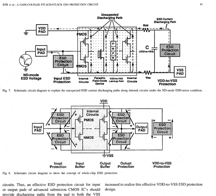
KER et al.: A GATE-COUPLED PTLSCR/NTLSCR ESD PROTECTION CIRCUIT 41
Fig. 7. Schematic circuit diagram to explain the unexpected ESD current discharging paths along internal circuits under the ND-mode ESD-stress condition. VDD
1
lnupt Input output Outupt VDD-to-VSS
Protection Buffer Buffer Protection Protection Fig. 8. Schematic circuit diagram to show the concept of whole-chip ESD protection.
circuits. Thus, an effective ESD protection circuit for input or output pads of advanced submicron CMOS IC’s should provide discharging paths from the pad to both the VSS and VDD lines. This is especially necessary for a CMOS VLSI/ULSI with a larger die size and much longer VDD and VSS power lines [25]. A schematic circuit diagram to explain the concept of whole-chip ESD protection is shown in Fig. 8. Providing whole-chip ESD protection design including consideration of VDD and VSS power lines will prevent ESD damage in the internal circuits of a CMOS IC.
Recently, another method to reduce the danger of ESD damage in internal circuits is to provide a more efficient VDD-to-VSS ESD protection circuit [28]-[33]. In [28]-[30], a control circuit based on
RC
time constant is designed to turnon
a
short-channel thin-oxide NMOS device, con- nected between the VDD and VSS power lines. To effectively bypass ESD current through the turned-on NMOS without causing damage on itself, such a short-channel thin-oxide NMOS is designed with a device dimension ( W L ) as large as 8000/0.8 (pm) [28]. Such a design can avoid ESD damage on the internal circuits, but the layout area has to be muchincreased to realize this effective VDD-to-VSS ESD protection design.
111. GATE-COUPLED PTLSCIUNTLSCR ESD PROTECTION CIRCUIT
To effectively protect the thinner gate oxide of deep- submicron low-voltage CMOS IC’s while avoiding ESD damage in internal circuits, a new ESD protection circuit is presented. This ESD protection circuit combines both the advantages of complementary-LVTSCR devices which provide highest ESD protection capability within smallest layout area [18] and the much lower trigger voltage by using a gate-coupling technique [ 151.
A. Circuit Configuration and Device Structures
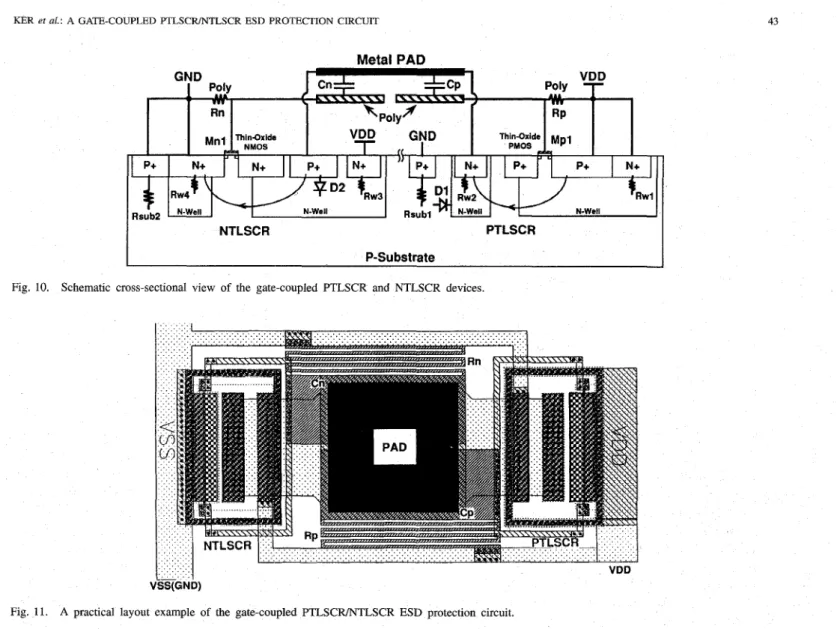
The proposed ESD protection circuit is shown in Fig. 9
with the corresponding cross-sectional view in Fig. 10. A
practical layout example is shown in Fig. 11. In Fig. 9, there is one PMOS-triggered lateral SCR (PTLSCR) device between the pad and VDD and one NMOS-triggered lateral SCR (NTLSCR) device between the pad and VSS. The PTLSCR
IEEE JOURNAL OF S
lead to a lower trig The coupled voltage o
longer in time by the on the PTLSCR and be realized by the poly occupying extra layout
ar
There are two parasitic
another N-well
P+ diffusion
d
voltage clamping. P-substrate are a1pact layout style for this ESD pr 42 Gate-Coupled PTLSCR circuits Gate-Coupled NTLSCR
CIUNTLSCR ESD protection cir- cult.
in-oxide PMOS (Mpl) into a lateral S lower its trigger voltage. In -I diffusion) is made across the junction of an N-well and the P-substrate as shown in Fig. 10. The trigger voltage of the PTLSCR is equivalent to
D [18]. The NTLSCR is made thin-oxide NMOS (Mnl) into a
snapback-breakdown voltage of the Mnl, if the gate of Mnl is connected to VSS [18]. The use of the N-well structure instead of just an
NS
diffusion, as the cathodes of PTLSCR and NTLSCR, is to enhance the emitter efficiency of lateraldrain snapback-breakdown to the gate-oxide breakdown voltage.
e is realized by the capacitors realized by the poly layer right under ncreasing total layout area of the pad.
are designed to couple suitable ESD- transient voltage to the gates of Mpl and Mnl, respectively.
specification.
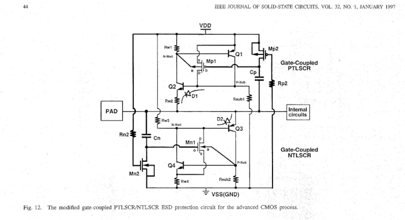
B. Modi$ed Desig
ESD current. To ESD transition, t be realized by the we Rp and Rn are realize suitable for the CMOS resistance, such as an
or Rn have the order about
digital CMOS process is sheet resistance of the p
KER et al.: A GATE-COUPLED PTLSCRINTLSCR ESD PROTECTION CIRCUIT 43
Metal
PAD Dd" Polv GYD N+ P+ N+ P+ N+/
OD*
t W 3 R w i N-Well N-Wall NTLSCR PTLSCR P-Substrate -Fig. 10. Schematic cross-sectional view of the gate-coupled PTLSCR and NTLSCR devices.
VSS(GND)
Fig. 1 1 . A practical layout example of the gate-coupled PTLSCIUNTLSCR ESD protection circuit.
or VSS lines to the gates of Mp2 and Mn2, even with a low poly sheet resistance.
C. Operating Principles
The operation of this modified gate-coupled PTLSCRNTLSCR ESD protection circuit is discussed below.
1 ) Normal Operating Conditions: Under normal CMOS operating conditions with VDD and VSS power supplies, Mp2 with its gate connected to VSS through a resistor Rp2 is turned on to bias the gate of Mpl at VDD, so the Mpl is off. This keeps the PTLSCR in its off state. Transistor Mn2, its gate connected to VDD through a resistor Rn2, is turned on to bias the gate of Mnl at VSS, so the Mnl is off. This keeps the NTLSCR also in its off state. Thus, the PTLSCR and the NTLSCR in the ESD protection circuit are guaranteed to be off under the normal CMOS operating conditions.
Moreover, the high-voltage level of input signals on the pad is clamped by the parasitic diode D2. When an input signal has a voltage overshoot greater than VDD, the diode D2 will be forward biased to clamp the overshooting voltage at around VDD
+
0.6 V. The low-voltage level of input signals on the pad is also clamped by the parasitic diode D l . When an input signal has a voltage undershoot below VSS, the diode D1will be forward biased to clamp the undershooting voltage at around VSS
-
0.6 V. Thus, the input signal is clamped between VDD+
0.6 V and VSS-
0.6 V. Thus, the PTLSCR and the NTLSCR are guaranteed not to be triggered on by the overshootinghndershooting input signals under the normal operating conditions. Diodes D1 and D2 are parasitically present in the PTLSCR and NTLSCR structures, respectively, as shown in Fig. 13. The current path in the forward-biased diodes is opposite to the conducting path of the PTLSCR and NTLSCR, so the layout can be drawn to keep the PTLSCR and NTLSCR off under the normal CMOS operating conditions.2) ESD-Stress Conditions: Since an ESD voltage on a pin may have positive or negative polarities to VDD or VSS, there are four modes of ESD stresses at each pin of a CMOS IC as shown in Fig. 6 . In the PS-mode ESD-stress condition (with grounded VSS but Aoating VDD), there is some positive ESD-transient voltage coupled to the gate of Mnl through the capacitor Cn. This coupled positive voltage on the gate
of
Mnl is designed to be above the threshold voltage of Mnl to turn it on. After the Mnl is turned on, the NTLSCR will be triggered on to bypass the ESD current. When the NTLSCR is triggered on, its holding voltage is only around 1 N 2 V. The positive ESD-stress voltage on the pad is clamped to around 1-
2 V, so the gate oxide of the input buffer can be fully protected. By44 IEEE JOURNAL OF SOLID-STATE CIRCUITS, VOL 32, NO 1, JANUARY 1997
Fig 12. The modified gate coupled PTLSCFUNTLSCR ESD protection circuit for the advanced C
suitably designing the c n, the ESD-transient voltage coupled to the gate of be controlled to adjust the ESD-trigger voltage of the NTLSCR for different applications. In the NS-mode (PD-mode) ESD stress, the parasitic diode D I (D2) is forward biased and turned on to bypass ESD current from the pad to VSS (VDD). The negative (positive) ESD- stress voltage on the pad is clamped to around
-0.6
-
-0.8 V(0.6 N 0.8 V), so the gate oxide of the input buffer can be fully
protected. A diode with proper layout in the forward-biased condition can perform high ESD robustness.
In the ND-mode ESD stress (with grounded VDD but floating VSS), there is some negative ESD-transient voltage coupled to the gate of Mpl through the capacitor Cp. This coupled negative voltage on the gate of Mp l is designed to turn the M p l on. After the Mpl is turned on, the PTLSCR will be triggered on to bypass the ESD current. When the PTLSCR is triggered on, its holding voltage is only around
- 1 N - 2 V. The negative ESD voltage on the pad is clamped
to around -1 N -2 V, so the gate oxide of the input buffer can be fully protected. By suitably designing the capacitor Cp, the gate of Mpl can be controlled to adju ESD-trigger voltage of the PTLSCR for different applications.
and ND) of ESD stresses are protected by the gate-coupled NTLSCR, D1, D2 and the gate-coupled PTLSCR devices. The ESD over-stress voltage
on the pad can be clamped by this proposed ESD protection circuit to very low voltage levels (only
f0.6
Nf2
V),so
the thinner gate oxide in deep-submicron low-voltage CMOS technologies can be fully protected.tion f o r Gate-Coupling Effect
In the PS-mode ESD stress, the VDD line is floating with an initial voltage close to the grounded VSS due to the P-
substratelN-well Initially, the Mn: coupled ESD-tra Gate-Coupled PTLSCR RP2 circuits Gate-Coupled NTLSCR
everywhere on the chip. high resistance to hold the the gate of Mnl to turn on the NTLSCR. Then, the p SD voltage is discharged by the NTLSCR. Befor ESD voltage is completely discharged, it may be diverted to the floating VDD power line through the diode D2 and the resistor Rw3 (or the PMOS device in CMOS output buffer, which is connected between the pad and VDD). This diverted ESD voltage on the VDD power line may bias the Mn2 and turn it on. Resistor Rn2 added between the gate of Mn2 and VDD will cause a t' delay to turn on the Mn2. Once on, the Mn2 acts as a resi to discharge the coupled voltage on the gate of M nl. A longer channel is used in the Mn2 to increase its turn-on resistance.
voltage of Mnl. A larger drain current in th
gate of Mnl and increasing
of Mnl above the threshold stress condition, but to c
capacitance increases also enhances the turn-on sp
KER et al.: A GATE-COUPLED PTLSCR/NTLSCR ESD PROTECTION CIRCUIT 45
Fig. 13.
Fig. 14. A layout
A similar design consideration is also applied to the Cp, Mpl, Mp2, and Rp2 in the gate-coupled PTLSCR device to bypass the ND-mode ESD stress.
IV. EXPERIMENTAL RESULTS
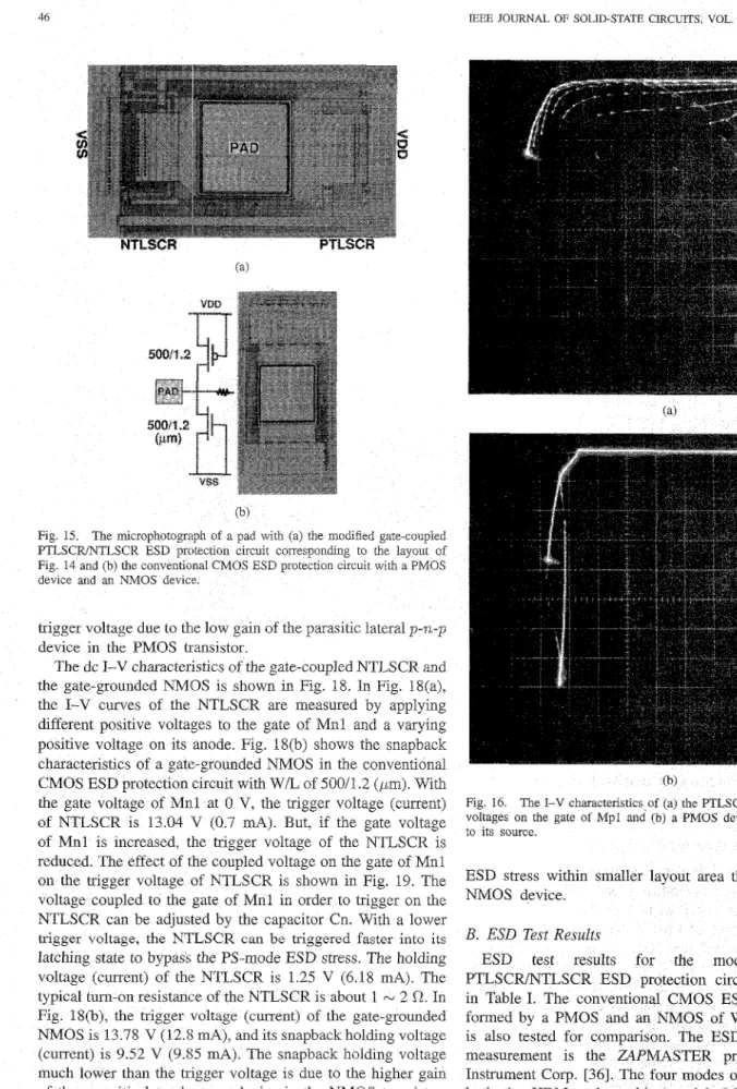
A test chip has been fabricated by using a 0.6-pm CMOS technology. A microphotograph of a pad with the modified
ESD protection circuit is shown in Fig. 1S(a), which is cor- responding to the layout of Fig. 14. The device dimensions
( W L ) of Mpl and Mnl are 7Y1.0 (bum). The coupling capacitor Cp (Cn) in the layout is about 0.4 pF, and the device dimensions of Mp2 and Mn2 are 10/10 (pm). In Fig. 15(b), a conventional CMOS ESD protection circuit formed by a PMOS and an NMOS with W/L = 500/1.2 (pm) is also tested as a reference in the same test chip. The spacing from the drain contact to the poly-gate edge is drawn as 5 pm in the
conventional CMOS ESD protection circuit.
A. Device Characteristics
The measured dc I-V characteristics of the gate-coupled PTLSCR and the gate-source-shorted PMOS in the conven-
tional CMOS ESD protection circuit are shown in Fig. 16. In Fig. 16(a), the I-V curves of the PTLSCR are measured by applying different negative voltages to the gate of Mpl with the VDD grounded, and the pad is stressed with a varying negative voltage. When the gate voltage of Mpl is 0 V, the trigger voltage (current) of the PTLSCR is -16.82 V (-12.35 mA). But, as the negative gate voltage of Mpl is increased, the trigger voltage of the PTLSCR is reduced as shown in Fig. 16(a). The effect of the coupled voltage on the gate of Mpl on the trigger voltage of PTLSCR is shown in Fig. 17. The voltage coupled to the gate of Mpl in order to trigger on the PTLSCR can be adjusted by the capacitor Cp. With a lower trigger voltage, the PTLSCR can be triggered faster into its latching state to bypass the ND-mode ESD stress. The holding voltage (current) of the PTLSCR is - 1.45 V (- 10.2 mA). The typical turn-on resistance of the PTLSCR is about
1 N 2 0. Fig. 16(b) shows the snapback characteristics of a
PMOS in the conventional CMOS ESD protection circuit with its gate connected to its source. The trigger voltage (current) of the PMOS with W/L of 500/1.2 (pm) is -15.58 V (-18.45 mA), and its snapback holding voltage (current) is -14.44
46
NTLSCR PTLSCR
Fig 15. The microphotog ph of a pad with (a) the modified gate-coupled PTLSCWNTLSCR ESD p tection circuit corresponding to the layout of Fig 14 and (b) the conventional CMOS ESD protectlon circuit with a PMOS device and an NMOS device.
trigger voltage due to the 1 n of the parasitic lateral p-n-p device in the PMOS tmnsistor.
The dc I-V characteristics of the gate-coupled NTLSCR and the gate-grounded NMlOS is shown in Fig. 18. In Fig. 18(a), the I-V curves of the NTLSCR are measured by applying different positive voltages to the gate of Mnl and a varying positive voltage on its anode. Fig. 18(b) shows the snapback characteristics of a gate-grounded NMOS in the conventional CMOS ESD protection circuit with W L of 500A.2 (pm). With the gate voltage of M a l at 0 V, the trigger voltage (current) of NTLSCR is 13.04 V (0.7 mA). But, if the gate voltage of Mnl is increased, the trigger voltage of the NTLSCR is reduced. The effect of {he coupled voltage on the gate of Mnl on the trigger voltage of NTLSCR is shown in Fig. 19. The to the gate of Mnl in order to trigger on the e adjusted by the capacitor Cn. With a lower LSCR can be triggered faster into its the PS-mode ESD stress. The holding NTLSCR is 1.25 V (6.18 mA). The e of the NTLSCR is about 1 N 2 0 . In Fig. 18(b), the trigger voltage (current) of the gate-grounded NMOS is 13.78 V (12.8 mA), and its snapback holding voltage (current) is 9.52 V (9.85 mA). The snapback holding voltage much lower than the trigger voltage is due to the higher gain of the parasitic lateral n-p-n device in the NMOS transistor. The holding voltage of NTLSCR is lower than that of the gate-grounded NMOS, so the ESD power dissipation in the
NTLSCR is much lower than that in the gate-grounded NMOS.
This IS the main reason why an NTLSCR can sustain higher
E E E JOURNAL OF SOLID-STATE CIR ANUARY 1997
to its source.
ESD stress within smaller la
NMOS device.
B. ESD Test Results
PTLSCWNTLS
is also tested for c measurement is th
exceeds 1 pA under 5-V
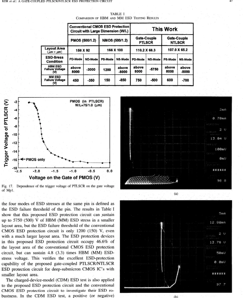
KER et a1 ' A GATE-COUPLED F'rLSCRINTLSCR ESD PROTECTION CIRCUIT 41 HEM ESD FailureVoltage MM ESD Failurevoltage (U) (v) TABLE I
COMPARISON OF HBM AND MM ESD TESTING RESULTS
This Work
Conventional CMOS ESD Protection Circuit with Large Dimension (WIL)
I
above 3000 1200 above above -5750 above above
8000 -8000 8000 aooo -8000
450 -350 150 -850 750 5 0 0 600 -700
I
I
PM08 (500/1.2)I
NMOS (50011.2)I
G;Fs$e
I
GateCouple NTLSCRg)
- 1 0 -m
>
L - 1 4 - a c1).-
U) -16 c-
-12 L 166 X 100 11 0.2 X 68.3 107.0 X 65.2 ii
*** - @.. h......*....+. ..-*..
...
.-.
-0% -+PMOS onlyI
I
PD-Mode1
ND-Mode1
PS-ModeI
NS-ModeI
PDMode1
ND-ModeI
PS-ModeI
NS-ModeI
PMOS (in PTLSCR) W/L.=75/1.0 (prn)
I
-2.0 -1.5 -1 .o -0.5 0.0 I- 4 8 1 -2.5Voltage on the Gate of PMOS (V)
Fig. 17. of Mpl.
Dependence of the trigger voltage of PTLSCR on the gate voltage
the four modes of ESD stresses at the same pin is defined as the ESD failure threshold of the pin. The results in Table I
show that this proposed ESD protection circuit can sustain up to 5750 (500) V of HBM (MM) ESD stress in a smaller layout area, but the ESD failure threshold of the conventional CMOS ESD protection circuit is only 1200 (150) V, even with a much larger layout area. The ESD protection devices in this proposed ESD protection circuit occupy 46.6% of
the layout area of the conventional CMOS ESD protection circuit, but can sustain 4.8 (3.3) times HBM (MM) ESD- stress voltage. This verifies the excellent ESD-protection capability of the proposed gate-coupled PTLSCIUNTLSCR ESD protection circuit for deep-submicron CMOS IC's with smaller layout area.
The charged-device-model (CDM) ESD test is also applied to the proposed ESD protection circuit and the conventional
CMOS ESD protection circuit to investigate their ESD ro-
bustness. In the CDM ESD test, a positive (or negative) ESD voltage is applied to the substrate by the ZAPMASTER socketed tester. The CDM ESD takes place when the input pad is grounded. A target of &1000 V is commonly used as an acceptable CDM ESD level for IC products. The CDM ESD test results are listed in Table 11. The positive CDM ESD level
(h) Fig. 18.
voltages on the gate of Mnl and (h) a gate-grounded NMOS device. of the conventional CMOS ESD protection circuit is greater than 2000 V because the NMOS device in the CMOS ESD The I-V charactenstics of (a) the NTLSCR with different positive
48
was reported that an 1-VTSCR device stands a low positive
IEEE JOURNAL OF SOLID-STATE CIRCUITS, VOL 32, NO 1, JANUARY 1997
I I 1
7 ns, which is close An oscilloscope is a negative pulse o
of HBM ESD eve
minimum voltage peak of the applied voltage pulse to
in Fig. 20(b). It is shown in Fig. 20(b)
Mpl is as high as -16.8
Similar experimental s
ESD-trigger voltage of the the PS-mode ESD-stress c is shown in Fig.
determined. The typical me on the gate-coupled NT
circuit is shown in Fi
positive voltage pulse NTLSCR, while the the gate of Mnl is as
V (7.03 V) in the
The trigger voltage devices also has e
D. Input Leakage The leakage curr circuit connected t the comparison of 1
KER et ab: A GATE-COUPLED PTLSCIUNTLSCR ESD PROTECTION CIRCUIT 49
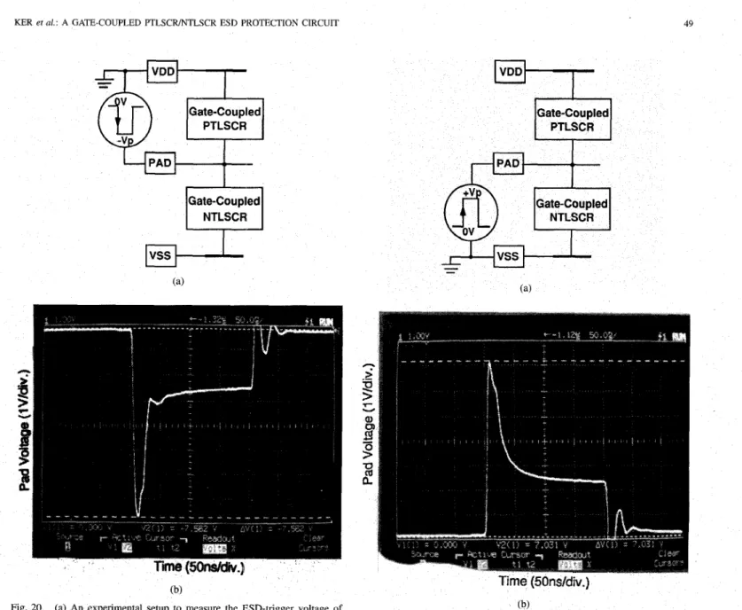
Gate-Coupled PTLSCR
Gate-Coupled NTLSCR
Fig. 20. (a) An experimental setup to measure the ESD-trigger voltage of the gate-coupled PTLSCR device in the ND-mode ESD-stress condition. (b) The measured voltage waveform at the pad as the gate-coupled PTLSCR is triggered on by the applied negative voltage pulse.
gate-coupled PTLSCIUNTLSCR ESD protection circuit and the conventional CMOS ESD protection circuit. The leakage current is measured (using an HP4145) by applying a voltage ramp from 0 V to 5 V to the input pad with 5-V VDD and 0-V VSS bias condition. In the line A of Fig. 22, the maximum input leakage current at 5-V bias in the gate-coupled PTLSCFUNTLSCR ESD protection circuit is only 1.7 pA. The
maximum input leakage current in the conventional CMOS ESD protection circuit is up to 10.5 pA (the line B in Fig. 22). The input leakage current is related to the diffusion area connected to the pad. The layout area of the gate- coupled PTLSCRNTLSCR ESD protection circuit is only 0.47 times that of the conventional CMOS ESD protection circuit, and hence the leakage current in the gate-coupled PTLSCIUNTLSCR ESD protection circuit is lower. Moreover, the input junction capacitance is also related to the diffusion area connected to the pad. The input capacitance of this gate- coupled PTLSCRAVTLSCR ESD protection circuit is therefore
(b)
Fig. 21. (a) An experimental setup to measure the ESD-trigger voltage of the gate-coupled NTLSCR device in the PS-mode ESD-stress condition. @) The measured voltage waveform at the pad as the gate-coupled NTLSCR is tnggered on by the applied positive voltage pulse.
smaller than that of the conventional CMOS ESD protection circuit. With low leakage current and low input capacitance, as well as without a resistor between the pad and internal circuits, this gate-coupled PTLSCFUNTLSCR ESD protection circuit is more suitable to protect the output or input pins o f analog IC's in high-precision applications.
V. CONCLUSION
By understanding both the turn-on mechanism of a lateral SCR device [34] and the capacitor-coupling design [35], the gate-coupling technique is merged into LVTSCR devices to
invent an effective ESD protection circuit for deep-submicron low-voltage CMOS IC's without any process modification. A practical design example of the proposed gate-coupled PTLSCFUNTLSCR ESD protection circuit has been success- fully verified. The ESD trigger voltage of the gate-coupled F'TLSCR and NTLSCR devices can be modified by adjusting
50
circuit can also be merged t buffer to effectively pro-
The authors wish Associate Editor C. Svensson and his reviewers for their valuable suggestions to revise this PaPe
REFERENCES
[SI C. Duvvury and A. Amerasekera, “ESD A pervasive reliability concern IC technologies,” Proc. IEEE, vol. 81, pp. 690-702, May 1993. Amerasekera and (3 Du y, “The impact of technology scaling ESD robustness and pro on circuit design,” in EOS/ESD Symp
Ker, H -H Chmg, and C.-Y. Wu, “ESD protection for deep- gate-couple CMOS-trigger lateral
, “Hot-electron reliability and ESD latent damage,” IEEE Trans. Electron Devices, vol. 35, pp. 2189-2193,
Dec. 1988.
[5] C Hu, S C. Tam, E’-C Hsu, P K KO, T Y Chan, and K. W. Terrill, “Hot-electron induced MOSFET degradation-Model, monitor,
Proc , 1994, vol EOS-16, pp 237-245
[31
1995, pp 543-546
improvement,” IEEE J Solid-State Czvcuiti, vol. SC-20, no. 1, pp. 295-305, 1985.
143-148
191 I. Kurachi, Y Fukuda, N Miura, and F Ichikawa, “Analysis of soft breakdown falure with ESD on output buffer nMOSFET’s and its
IEEE JOURNAL OF SOLID-STAT
pp 141-150
, “EOSRSD reliability of in Proc. IRPS, 1995, pp
using capacitor-couple technique in 0 5-mm 3-
ASIC Con$, Exhibit, 19
~, “Whole-chip ESD protection for CMOS VLSILJLSI with mul- tiple power pins,” in Proc: IEEE Int. Integrated Relzabzlztv Workshoa.
resistance of on-chip power supply buses on internal device falure after ESD stress,” IEEE Trans.
Nov. 1993.
mcron gate arrays,” in EOS [26] M. Yancey, “Automatic pl
286-291
IEEE Trans VLSI Syst.,
[37] C Duvvury and A Am EOS-17, gp 162-174
KER et a1 A GATE-COUPLED PTLSCWTLSCR ESD PROTECTION CIRCUIT 51 Ming-Dou Ker (S’92-M’94) was born in Taiwan,
R.O.C., in 1963. He received the B.S. degree from the Department of Electronics Engineering, National Chiao-Tung University, Hsinchu, Tawan, and the M S and Ph D degrees from the Institute of Elec- tronics, National Chiao-Tung Universlty, Hsinchu, Tawan, in 1986, 1988, and 1993, respectively
From 1993 to 1994 he was a postdoctoral re- searcher m the Integrated Circuits and Systems Laboratory, Institute of Electronics, Nabonal Chiao- Tunc Universitv, Hsmchu. Taiwan. In 1994, he Y
joined the VLSI Design Department of Computer and Communication Re- search Laboratories (CCL), Industnal Technology Research Institute (ITN), Hsinchu, Taiwan, as a Circuit Design Engineer Since then he has been engaged in the development of mixed-mode integrated circuits in submicron CMOS technology He also has 12 patents including five U S patents Hls research interests include reliability of CMOS integrated circuits, mxed-mode integrated circuits, and communicatlon integrated circuits design
Hun-Hsien Chang (S’93) was born in Taipei, Tai- wan, R.O.C., in 1964. He received the B.S. degree from the Department of Electronics Engineering, National Chiao-Tung University, Hsinchu, Taiwan, in 1991
Presently, he is working toward the Ph D degree in the Institute of Electronics, National Chiao-Tung University. His current research interests include I/O interface circuit, ESD protectlon circuit, and CMOS mixed-mode IC’s for high-speed data communica- tions.
Chung-Yu Wu (S’75-M’77-SM’96) was born in Chiayi, Taiwan, R.O.C., in 1950. He received the M.S. and Ph.D. degrees from the Department of Electronics Engineenng, National Chiao-Tung Uni- versity, Tawan, in 1976 and 1980, respectively.
From 1980 to 1984 he was an Associate Profes- sor in the National Chiao-Tung University. During 1984-1986 he was a Visiting Associate Professor in the Department of Electrical Engineering, Portland State University, OR. Since 1987, he has been a Professor in the National Chiao-Tung Universitv From 1991 to 1995, he was rotated to serve as Director of thi D Engineering and Applied Science in the National Science Council. Currently, he is the Centennial Honorary Chair Professor at the National Chiao-Tung University. He has published more than 70 journal papers and 100 conference papers on several topics, including digital integrated circuits, analog integrated circuits, computer-aided design, neural networks, ESD protection circuits, special semiconductor devices, and process technologies. He also has 17 patents, including eight U S . patents. His current research interests focus on low-voltage, low-power, mixed-mode integrated circuit design, hardware implementation of visual and auditory neural systems, and RF integrated circuit design.
Dr. Wu is a member of Eta Kappa Nu and Phi Tau Phi. He was awarded the Outstanding Research Award by the National Science Council in 1989 and 1995, and the Outstanding Engineering Professor by the Chinese Engineer Association in 1996.
![Fig 4 Schematic cross-sectional view of the LVTSCR device [17] VDD](https://thumb-ap.123doks.com/thumbv2/9libinfo/7632301.135395/3.929.237.868.16.683/fig-schematic-cross-sectional-view-lvtscr-device-vdd.webp)