Electroless deposition of Ru
films on Si substrates with surface pretreatments
Jing-Yu Chen, Shiau-Lin Huang, Pu-Wei Wu
⁎
, Pang Lin
Department of Materials Science and Engineering, National Chiao Tung University, Hsinchu 300, Taiwan
a b s t r a c t
a r t i c l e i n f o
Available online 9 June 2012 Keywords:
Electroless deposition Rufilm
Si substrate Surface pretreatment
Electroless Ru depositions on Si substrates undergoing surface pretreatments such as hydrogenfluoride (HF) etching, HF etching and activation, as well as HF etching, sensitization, and activation are explored. The plat-ing bath contains K2RuCl5∙xH2O, NaClO, NaOH, and NaNO2at appropriate ratios. Continuous electroless Ru
film is unable to obtain on the as-received Si wafer because the native oxide inhibits the process of nucleation and growth. In contrast, after surface pretreatments, dense and continuous Rufilms are observed at reason-able growth rates. Contact angle measurements indicate a relatively hydrophilic surface after sensitization and activation, which leads to faster Rufilm growths and larger surface roughness as compared to the HF-etched sample. X-ray photoelectron spectra confirm the formation of Sn and Pd nuclei and their presence promotes the heterogeneous growth of Rufilms as evidenced by images from scanning electron microscope. In addition, depth profiling from Auger electron spectrometer suggests a uniform composition across the film thickness despite part of the Ru exists in an oxidized form.
© 2012 Elsevier B.V. All rights reserved.
1. Introduction
Ruthenium (Ru) and ruthenium oxide (RuO2) have attracted
con-siderable attention recently because of their unique physical and chem-ical properties for many industrial applications. For example, Ru is explored as a diffusion barrier layer and as an electrocatalyst in semi-conductor and electrochemical devices, respectively[1,2]. In addition, RuO2is widely studied as a promising pseudocapacitive material[3].
Conventional synthetic routes for Ru and RuO2involve vacuum-based
and solution-based approaches. The vacuum-based technique includes physical vapor deposition [4], chemical vapor deposition[5,6], and atomic layer deposition[7–9]. Unfortunately, these processes often re-quire expensive equipment and they are known for unnecessary pre-cursor waste. In contrast, the solution-based approach such as sol–gel synthesis [10], electroplating [3,11,12], and electroless deposition
[13–19]are credited with simple setups, efficient use of precursors, as well as scalability in outputs. In the solution-based approach, the ele-ctroplating technique can be conducted via an externally applied driv-ing force in potentiostatic or galvanostatic mode to direct deposits on conductive substrates. In contrast, the electroless deposition technique can be applied on both conductive and non-conductive platforms as re-ducing agents in the plating bath are responsible for rere-ducing ions on the substrates instead.
In principle, the electroless deposition approach involves an auto-catalytic reaction to form deposits via a heterogeneous nucleation and growth[20]. Notable advantages for the electroless deposition
technique are wide substrate selection, sophisticated shape tolerance, and free of externally applied driving force. To date, electroless depo-sition of metals including Ni, Cu, Ag, Au, Pd, and Pt have been demon-strated in various formulations and their formation mechanisms are well-established[21–25]. On the other hand, metals such as Ru, Rh, Re, Os, and Ir have received few attention and functional ele-ctroplating baths still require further investigation[26]. In the case of Ru, preliminary experiments have been carried out on substrates including Cu, C, Pd-InGaAs, Si, and acrylonitrile butadiene styrene
[13–19]. It is realized that for non-conductive substrates, selective surface pretreatments are rather necessary to ensure a uniformfilm formation. Earlier, Chang et al. attempted Ru electroless deposition on Si substrates but surface pretreatments were not discussed[15]. Recently, we have developed an oxidative–reductive Ru electroless plating bath and demonstrated its applicability on a Cu substrate
[18,19]. Since Cu is known as a conductive surface for electroless plat-ing, it becomes our interest to explore identical formulation on non-conductive surface such as Si. Preliminary study using as-received Si substrates concluded that a dense Ru film was unable to form. Hence, in this work, we investigate the effect of surface pretreatments on Si substrates for the formation of continuous Rufilm via an elec-troless route.
2. Experimental details
A 6-inch boron doped p-type single crystalline Si wafer with (100) orientation was broken into small pieces (2 × 2 cm2) and they were
used as the substrates for Ru electroless deposition. The resistance and thickness for the Si wafer were 1–30 Ωcm and 625±25 μm, re-spectively. Prior to surface pretreatment, the Si samples were rinsed
Thin Solid Films 529 (2013) 426–429
⁎ Corresponding author.
E-mail address:[email protected](P.-W. Wu).
0040-6090/$– see front matter © 2012 Elsevier B.V. All rights reserved. doi:10.1016/j.tsf.2012.06.014
Contents lists available atSciVerse ScienceDirect
Thin Solid Films
with deionized water and acetone to remove any debris and possible contaminant. Afterward, it was immersed in a hydrogenfluoride (HF) solution at 25 °C for 10 min. The HF solution contained HF (J.T. Baker; Buffered Oxide Etch 6:1) and H2O2(SHOWA; 35 wt.%) at a 1:50
vol-ume ratio. Subsequently, the Si samples were further subjected to two different steps including activation, as well as sensitization and activation, respectively. The activation step involved immersing the Si substrate in a mixture of 0.1 wt.% PdCl2and 1 wt.% HCl in deionized
water at 40 °C for 10 min. The sensitization step engaged the Si sub-strate in a solution containing 0.3 wt.% SnCl2 and 2.5 wt.% HCl in
deionized water at 25 °C for 3 min. Upon completion of surface pre-treatments, the samples were submerged in a Ru electroless plating bath at 40 °C for different times. The chemical ingredients in the plat-ing bath contain K2RuCl5∙xH2O, NaClO, NaOH, and NaNO2at
appropri-ate ratios, and the relevant oxidative–reductive mechanism for Ru film formation has been reported elsewhere[18].
Afield-emission scanning electron microscope (FE-SEM; JEOL-JSM-6500F) with 15 keV operating voltage was used to observe morphology and thickness for the depositedfilms. We took the cross-sectional SEM images and selected three different locations to estimate their respec-tive heights. An energy dispersive spectrometer (EDS; Oxford 7557) was utilized for elements detection. The acceleration voltage was 15 keV and the acquisition time was 70 s for the EDS measurement. A contact angle set-up consisting of lens, light source, and a power supply was adopted to determine hydrophilicity of Si substrates before and after surface pretreatments. An atomic force microscope (AFM; Vecco Dimension 5000 Scanning Probe Microscopy) was involved to deter-mine roughness for the depositedfilms. Tapping mode was utilized for AFM measurement for 1 × 1μm2scanning area. An Auger electron
spectrometer (AES, Thermo Microlab 350) was employed to perform depth profiling for the deposited films. The depth profile was divided into 100 layers with Ar ions bombardment at 5 s per layer. An X-ray photoelectron spectrometer (XPS; Thermo Microlab 350) with Mg tar-get was used to identify oxidation states of Sn and Pd on Si substrates after surface pretreatments. For the XPS measurements, additional Pt particles were sputtered on the Si surface serving as a standard for cor-rection with metallic Pt binding energy at 4f7/2at 71.2 eV. The Si surface
was bombarded with Ar ions which were operated with 3 kV and 1μA for 30 s before recording the XPS.
3. Results and discussion
Table 1provides the contact angles for Si samples before and after surface pretreatments, as well as the roughness before and after Ru electroless depositions. As listed, the removal of native oxide from the as-received Si wafer after HF etching rendered a relatively hydro-phobic surface. However, after further pretreatments of activation or sensitization and activation, the Si surfaces were transformed to hy-drophilic again. The roughness values were consistent with what we expected as activation steps produced Pd nuclei that led to a larger roughness especially for the sample undergoing sensitization and ac-tivation steps. In addition, after Ru electroless deposition, more Pd nuclei on the Si surface resulted in a larger thickness variation for the deposited Ru.
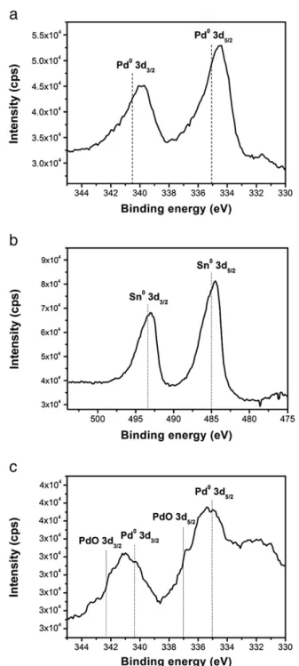
Fig. 1demonstrates the XPS profiles for the Si samples after surface pretreatments. As shown inFig. 1(a), the Pd 3d5/2and 3d3/2were
iden-tified at 334.4 and 339.9 eV, respectively for the Si substrate after acti-vation pretreatment. These values agree well with what was reported earlier for metallic Pd 3d lines[27]. Hence, we realize that the activa-tion step is effective in distributing Pd nuclei on the Si surface for sub-sequent Ru deposition.Fig. 1(b) and (c) exhibits the Sn 3d and Pd 3d lines after sensitization and activation pretreatments, respectively. As shown inFig. 1(b), the profile revealed notable signals at 484.5 and 493.4 eV, which are consistent with metallic Sn from literature
[27]. In addition, there were presence of Pd 3d lines at 335.4 and 341.1 eV, and these values are slightly larger than those inFig. 1(a), in-dicating that moderate Pd oxidation to PdO was possibly occurring
[28,29]. The shoulder at 332 eV inFig. 1(c) is from Pt 3d3/2which is
Table 1
Contact angles for Si samples before and after surface pretreatments, as well as rough-ness before and after 30 min Ru electroless depositions.
Contact angle (°)
Roughness (nm)
Before Ru deposition After Ru deposition As-received Si substrate 37.97 0.2 N/A
HF etching 79.75 0.3 3.72
HF etching + activation 17.08 3.6 11.61 HF etching + sensitization
+ activation
12.84 4.3 11.79 Fig. 1. XPS profiles for Si samples (a) after activation pretreatment for Pd 3d lines, as well as (b) after sensitization and activation pretreatments for (b) Sn 3d lines and (c) Pd 3d lines.
427 J.-Y. Chen et al. / Thin Solid Films 529 (2013) 426–429
attributed to the sputtered Pt prior to the XPS measurements. Our re-sults suggest that metallic Sn and oxidized Pd are formed on the Si sur-face after sensitization and activation treatments.
In order to confirm the formation of Ru films on the Si sample, the EDS was employed after 15 min of plating time. The estimated Ru amounts for activation as well as sensitization and activation were 1.06 and 0.93 at.%, respectively. In contrast, the Si sample after only HF etching was merely 0.81 at.%. Earlier, XPS results on the plated films atop Cu substrates indicated a composition makeup of 92.5 at.% Ru and 7.5% RuO2[19]. Since we used identical plating formulation to
carry out electroless deposition in this study, we believe that the resulting composition was not notably altered from previous work. The acceleration voltage for the EDS is 15 keV, which is in line with what are typically used in similar measurements. Hence, the signal depth for element detection in EDS is likely to be several micrometers. Considering that the thickness for the plated Rufilms was only in sub-micron regime (b100 nm), it is not unexpected that the recorded Ru amount in terms of atomic percentage was largely subdued.
Fig. 2presents the SEM images of Rufilms after 40 min of electro-less plating. As shown inFig. 2(a), the as-received Si wafer revealed Ru deposit that was partially formed. Previously, we purchased wa-fers with 500 nm SiO2on surface and determined that with or
with-out surface treatments (HF etching, hydrophilic silane treatment, etc.), the Rufilms were unable to deposit. This is because the SiO2is
known to be unstable in alkaline solution and the pH value for the Ru plating bath is 12–13. Thus, nucleation and growth of stable nuclei are unable to proceed as the underlying SiO2keeps dissolving during
electroless plating. Since the Si wafer always has a native SiO2on its
surface (~3 nm), surface pretreatment is thus necessary to render it more susceptible to Ru deposition. As shown inFig. 2(b), Si sample after HF etching revealed a relativelyflat Ru film with scattered parti-cles atop. In contrast, for Si samples after HF etching and activation, as well as HF etching, sensitization, and activation shown inFig. 2(c) and
(d), respectively, the Rufilms demonstrated granular morphologies with notable thickness variations. These results are not unexpected since the presence of nuclei promotes heterogeneous island growths that coalescence into a solidfilm eventually. This mechanism is sub-stantiated by the apparent voids observed inFig. 2(c).
Fig. 3provides the average thickness and standard deviation for the Rufilms on Si samples after surface pretreatments. Apparently, a linear relationship between the deposition time andfilm thickness was observed for all samples. To accurately estimate the growth rate, thefirst data point at 15 min was excluded. As a result, the remaining data points lead to y = 27.44 + 1.07x, R2= 0.94 for HF
etching, y = 25.35 + 1.53x, R2= 0.98 for HF etching and activation, and y = 17.03 + 1.85x, R2= 0.99 for HF etching, sensitization, and
ac-tivation. Obviously, the slower growth rate observed for the HF etch-ing sample is attributed to the lack of nucleation sites for Ru electroless deposition. An alternative possibility is the relatively hy-drophobic surface that discourages wetting of Ru plating bath. For samples undergoing additional sensitization and activation steps, there appeared a slightly faster growth rate as compared to those of activation step, which is rationalized by its excessive Sn and Pd nuclei on the Si surface. However, we must admit that the effect of sensitiza-tion seems to be rather moderate.
Fig. 4presents the AES depth profile for the Ru film after 30 min of electroless plating on the Si sample undergoing HF etching, as well as sensitization and activation. The atomic percentage for Ru was clearly observed when the etching time was varied from 0 to 330 s. Assum-ing the etchAssum-ing rate of standard SiO2(2 Å s− 1) is identical to that of
Ru, the thickness for the Rufilm is estimated at 66 nm. This value is reasonably close to what was observed in SEM cross-sectional view at 71.9 ± 9.5 nm. As shown in the depth profile, from 0 to 25 s the atomic percent for O was slightly larger than that for Ru, suggesting that the surface for the Rufilm was partially oxidized becoming Ru oxide or hydroxide instead. This behavior is not unusual as the Ru is
Fig. 2. SEM images of Rufilms after 40 min of electroless plating for the (a) as-received Si substrate, and Si substrates undergoing (b) HF etching, (c) HF etching and activation, and (d) HF etching as well as sensitization and activation.
known to form RuOxand Ru(OH)xwhen it is exposed to atmosphere
or electrolyte. When the etching time was between 25 and 145 s, the atomic percentage for Ru and O remained relatively unchanged at 40– 50%, inferring that the composition for the Rufilm was rather uni-form. According to our previous work[19], the electroless Ru plating bath produces a composite Ru/RuO2 film and the exact Ru/RuO2
makeup is contingent on the processing parameters involved. There-fore, it is likely to have this amount of oxygen throughout the depos-itedfilm. Lastly, when the etching time was between 145 and 330 s, the atomic percentage for Si became larger than those of Ru and O. This behavior was caused primarily by surface roughness at the inter-face between Si and Ru that renders both signals to be detected simultaneously. Another remote possibility is the formation of sili-cides such as RuSi or Ru2Si3because the binary phase diagram of Ru
and Si indicates so when the Ru/Si ratio is larger than 1[30]. Howev-er, since our samples were not subjected to any heat treatment after the electroless depositions, the formation of intermetallic ruthenium silicide was very unlikely.
4. Conclusions
We explored electroless Ru depositions on Si substrates undergoing surface pretreatments including HF etching, sensitization, and activation.
Contact angle measurements indicated a relatively hydrophilic surface after sensitization and activation, which led to faster Rufilm growths and larger surface roughness as compared to the HF-etched sample. XPS confirmed the formation of Sn and Pd nuclei and their presence facilitated the heterogeneous growth of Rufilms. Results from AES depth profiling suggested a uniform composition across thefilm thickness despite part of the Ru was present in an oxidized form. We determined that without surface pretreatment, Rufilm was not able to form. In contrast, after HF etching, sensitization, and activation, dense Rufilms were obtained at rea-sonable growth rates.
Acknowledgments
Financial support from the National Science Council of Taiwan (100-ET-E-009-002-ET) is noted.
References
[1] K. Frohlich, K. Husekova, D. Machajdik, J. Hooker, N. Perez, M. Fanciulli, S. Ferrari, C. Wiemer, A. Dimoulas, G. Vellianitis, Mater. Sci. Eng., B 109 (1–3) (2004) 117.
[2] U. Paulus, U. Endruschat, G. Feldmeyer, T. Schmidt, H. Bonnemann, R. Behm, J. Catal. 195 (2) (2000) 383.
[3] C.C. Hu, Y.H. Huang, J. Electrochem. Soc. 146 (7) (1999) 2465.
[4] T. Aoyama, A. Murakoshi, M. Koike, S. Takeno, K. Imai, Jpn. J. Appl. Phys. 37 (1998) 242. [5] J.M. Lee, J.C. Shin, C.S. Hwang, H.J. Kim, C.G. Suk, J. Vac. Sci. Technol., A 16/5 (1998)
2768.
[6] J.H. Shin, A. Waheed, W.A. Winkenwerder, H.W. Kim, K. Agapiou, R.A. Jones, G.S. Hwang, J.G. Ekerdt, Thin Solid Films 515 (13) (2007) 5298.
[7] S. Noh, S. Lee, E. Kim, Y. Kong, Curr. Appl. Phys. 6 (2) (2006) 171.
[8] S.K. Kim, S.Y. Lee, S.W. Lee, G.W. Hwang, C.S. Hwang, J.W. Lee, J. Jeong, J. Electrochem. Soc. 154 (2) (2007) D95.
[9] J.H. Kim, D.S. Kil, S.J. Yeom, J.S. Roh, N.J. Kwak, J.W. Kim, Appl. Phys. Lett. 91 (5) (2007) 052908.
[10] Y.H. Lee, J.G. Oh, H.S. Oh, H. Kim, Electrochem. Commun. 10 (7) (2008) 1035. [11] I.H. Kim, J.H. Kim, Y.H. Lee, K.B. Kim, J. Electrochem. Soc. 152 (11) (2005)
A2170.
[12] C.C. Hu, M.J. Liu, K.H. Chang, J. Power Sources 163 (2) (2007) 1126.
[13] Y. Okinaka, C. Wolowodiuk, in: G.O. Mallory, J.B. Hajdu (Eds.), Electroless Plating: Fundamentals and Applications, American Electroplaters and Surface Finishers Society, Orlando, FL, 1990, p. 421.
[14] K. Okuno, Plat. Surf. Finish. 77 (2) (1990) 48.
[15] Y.S. Chang, M.L. Chou, J. Appl. Phys. 69 (11) (1991) 7848.
[16] M. Rarnani, B.S. Haran, R.E. White, B.N. Popov, J. Electrochem. Soc. 148 (4) (2001) A374.
[17] E.M. Lysczek, S.E. Mohney, J. Electrochem. Soc. 155 (10) (2008) H699. [18] J.-Y. Chen, L.-Y. Wang, P.-W. Wu, Thin Solid Films 518 (24) (2010) 7245. [19] J.-Y. Chen, Y.-C. Hsieh, L.-Y. Wang, P.-W. Wu, J. Electrochem. Soc. 158 (8) (2011)
D463.
[20] J. Rebelli, A.A. Rodriguez, S.G. Ma, C.T. Williams, J.R. Monnier, Catal. Today 160 (1) (2011) 170.
[21] M. Schlesinger, in: M. Schlesinger, M. Paunovic (Eds.), Modern Electroplating, John Wiley & Sons, New York, 2010, p. 447.
[22] M. Schlesinger, in: M. Schlesinger, M. Paunovic (Eds.), Modern Electroplating, John Wiley & Sons, New York, 2010, p. 433.
[23] M. Schlesinger, in: M. Schlesinger, M. Paunovic (Eds.), Modern Electroplating, John Wiley & Sons, New York, 2010, p. 131.
[24] Y. Okinaka, M. Kato, in: M. Schlesinger, M. Paunovic (Eds.), Modern Electroplating, John Wiley & Sons, New York, 2010, p. 483.
[25] I. Ohno, in: M. Schlesinger, M. Paunovic (Eds.), Modern Electroplating, John Wiley & Sons, New York, 2010, p. 477.
[26] T. Jones, Electroplating of the Lesser-known Precious Metals: Rhodium, Rutheni-um, IridiRutheni-um, RheniRutheni-um, OsmiRutheni-um, 2003, p. 3.
[27] J.F. Moulder, W.F. Stickle, P.E. Sobol, K.D. Bomben, in: J. Chastain, J.R.C. King (Eds.), Handbook of X‐ray Photoelectron Spectroscopy: a Reference Book of Standard Spectra for Identification and Interpretation of XPS Data, Physical Electronics, Eden Prairie, MN, 1995.
[28] T.H. Fleisch, G.J. Mains, J. Phys. Chem. 90 (21) (1986) 5317.
[29] A. Tressaud, S. Khairoun, H. Touhara, N. Watanabe, Z. Anorg. Allg. Chem. 541 (9–10) (1986) 291.
[30] T.B. Massalski, in: T.B. Massalski, H. Okamoto (Eds.), Binary Alloy Phase Diagrams, vol. 3, American Society for Metals, Metals Park, Ohio, 1995, p. 3253.
Fig. 3. Growth rate of Rufilms for Si samples undergoing (a) HF etching, (b) HF etching and activation, as well as (c) HF etching, sensitization and activation.
Fig. 4. AES depth profile for the Ru film after 30 min of electroless plating for Si sample undergoing HF etching, sensitization and activation.
429 J.-Y. Chen et al. / Thin Solid Films 529 (2013) 426–429