This article was downloaded by: [National Chiao Tung University 國立交通大 學]
On: 28 April 2014, At: 05:17 Publisher: Taylor & Francis
Informa Ltd Registered in England and Wales Registered Number: 1072954 Registered office: Mortimer House, 37-41 Mortimer Street, London W1T 3JH, UK
Integrated Ferroelectrics: An
International Journal
Publication details, including instructions for authors and subscription information: http://www.tandfonline.com/loi/ginf20
Electrical properties of O
2
and
N
2
annealed (Ba, Sr)TiO
3
thin
films
M. S. Tsai a , S. C. Sun ab & T. Y. Tseng a a
Department of Electronics Engineering , National Chiao Tung University , Hsinchu, Taiwan, R.O.C. b
Research and Development, Taiwan Semiconductor Manufacturing Company , Hsinchu, Taiwan, R.O.C. Published online: 19 Aug 2006.
To cite this article: M. S. Tsai , S. C. Sun & T. Y. Tseng (1998) Electrical properties of O2 and N2 annealed (Ba, Sr)TiO3 thin films, Integrated Ferroelectrics: An International Journal, 21:1-4, 173-183, DOI: 10.1080/10584589808202061
To link to this article: http://dx.doi.org/10.1080/10584589808202061
PLEASE SCROLL DOWN FOR ARTICLE
Taylor & Francis makes every effort to ensure the accuracy of all the information (the “Content”) contained in the publications on our platform. However, Taylor & Francis, our agents, and our licensors make no
representations or warranties whatsoever as to the accuracy, completeness, or suitability for any purpose of the Content. Any opinions and views
expressed in this publication are the opinions and views of the authors, and are not the views of or endorsed by Taylor & Francis. The accuracy of the Content should not be relied upon and should be independently verified with primary sources of information. Taylor and Francis shall not be liable for any losses, actions, claims, proceedings, demands, costs, expenses, damages, and other liabilities whatsoever or howsoever caused arising directly or
indirectly in connection with, in relation to or arising out of the use of the Content.
This article may be used for research, teaching, and private study purposes. Any substantial or systematic reproduction, redistribution, reselling, loan, sub-licensing, systematic supply, or distribution in any form to anyone is expressly forbidden. Terms & Conditions of access and use can be found at http://www.tandfonline.com/page/terms-and-conditions
Inrqrutrd Ferroi.lewrcs. 1998. Vol. 21. pp. 173-183 Reprints available directly from the publisher Photocopying permitted by license only
8 1998 OPA (Overseas Publishers Association) N.V. Published by llcense under
the Gordon and Breach Science
Publishers imprint. Printed in Malaysia.
Electrical Properties
of
0 2
and
N2
Annealed
(Ba,Sr)Ti03 Thin
Films
M.
S.
Tsai,
S.
C.
Sun*
and
T.
Y.
Tseng
Department of Electronics Engineering, National
Chiao
Tung University Hsinchu, Taiwan, R.O.C.*Research and Development, Taiwan Semiconductor Manufacturing Company Hsinchu, Taiwan,
R.O.C.
(Received 4 Murch 1998; In jinalform 3 May 1998 j
The dielectric constant and the leakage current of (Ba,Sr)TiO,
(BST)
thin films deposited on Pt boaom electrodes before and after annealing in 0, and N2 ambients were investigated. The crystallinity was improved after post- deposition annealing. The refractive index, dielectric constant, and leakage current of the films were strongly dependent on the annealing conditions. The 02-annealed BST films have higher dielectric constant and lower leakage current than those annealed inN2
ambient.Keywords:
BST;
annealing; oxygen vacancy; leakage currentINTRODUCTION
In recent years, thin films made &om high dielectric constant materials have attracted great attention for use in fabricating cell capacitors for high density dynamic random access memories (DRAMS), since employment of high- dielectric constant films can lower the height of the storage node and simplify the cell structure. The (Ba,Sr)TiO, (BST) films have been reported to be the most promising capacitors materials for giga-bit DRAMs because of its high dielectric constant, low leakage current density,
high
dielectric breakdown strength, paraelectric perovskite phase that does not exhibit fatigue and aging and the ease of compositional control [ 1-41,Pt
is the most studied electrode material because it has a large work function which lowers the leakage currentI73
I74 M. S . TSAl et al.
strength, paraelectric perovskite phase that does not exhibit fatigue and aging and the ease of compositional control [1-4].
Pt
is the most studied electrode material because it has a large work function which lowers the leakage current of BST capacitors. In this paper we have studied the electrical characteristics of annealed BST films onPt.
Electrical and reliability characteristics of BST films annealed at different conditions are compared.EXPERIMENTAL
Metal-BST-metal capacitors were
used
as test devices. Pt bottom electrode with thickness of 100 nm was directly deposited on SiO, coated Si-substrates by RF magnetron sputtering at 350 "C.
BST thin films (100 nm) were deposited by RF magnetron sputtering at 450 and 27"C
in ambient of 50% 0,and 50% Ar. After BST deposition, some samples were treated in 0, and N,
at 550,650 and 750°C for 1 to 3 min using rapid thermal annealing and 30 min using furnace annealing. Finally, Pt (50 nm) top electrodes with diameters of 165, 255 and 350 p were formed by electron beam evaporation through a
shadow mask. The refractive index and the film thickness of BST films before and after annealing were measured by Rudolph Auto
EL-III
ellipsometer at a wavelength of 6328A.
RESULTS AND DISCUSSION
Fig. I depicts the change of refractive index with annealing time for BST thin films deposited at 27 "C , The refractive index of BST annealed at 550
"C
approaches a constant value-
1.85. The refractive indexes of BST annealed at 650 and 750°C increase with increasing annealing time, but the index of BST annealed at 750 'C attains saturation when annealed over 1 min.Fig, 2 shows the variation of thickness with annealing time for BST thin films deposited on Pt at 27°C. The film thickness of BST annealed at 550 and 650°C decreases with increasing annealing time. Also the film thickness of BST annealed at 750°C decreases with increasing annealing time, but it attains saturation when annealed over 1 min. This thickness reduction can be explained as the result of an increased density and elimination of porosity [5].
ELECTRICAL PROPERTIES OF 0, AND N2 175
-0
T=65O0C
.f j
Ig
2.0
a
0
n 1 L L0
1
10
100
1 .uTime
(
min)
FIGURE
1 The refraction index of BST films deposited at 27"C
as a fimction of annealing time in N,.FIGURE 2 The thickness of BST films deposited at 27 "C as function of annealing time in
N,.
176 M. S. TSAI rt 01.
Fig. 3 indicates that the dielectric constant of 27 "C -deposited BST after
annealed at 550 'C in
N,
ambient approachs a constant value-
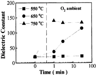
23. The dielectric constant of BST annealed at 650 and 750 "C increases with increasing annealing time, which may be due to the increase of crystallinity with annealing. However, the dielectric constant of BST annealed at 750°C attains saturation after annealing over 1 min. The results shown in Fig. 3 are in good agreement with those indicated in Fig. 1. Fig. 4 shows that the dielectric constant of BST annealed in 0, have the similar result with Fig. 3.The dielectric constant of BST annealed in 0, is larger than that of BST
annealed in N,. These results may be attributed to the lowering of the oxygen vacancy concentration in BST annealed in O,, which may lead to an increase in dielectric constant.
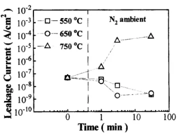
Fig. 5 illustrates the leakage current measured at 100 kV/cm (with 30 sec delay time) as a function of N2 annealing time. The leakage current of BST
annealed at 550
"C
decreases with increasing annealing time, because of increasing densification of BST films after post-annealing, as shown in Fig. 2. The leakage current of BST annealed at 650 "C decreases with increasing annealing time, but it slightly increases for BST films annealed for 30 min.The possible reason is that the increase in densification of BST
films
after post-annealing leads to a decrease of leakage current, but the increase of crystallinity for annealing over 30 min will increase the leakage current. The leakage current of BST annealed at 750°C increases with increasing annealing time, because the crystallinity effect is more dominant, as compared to the effect of densification. Also, morphology changes such as hillocks can greatly influence leakage after annealing at high temperature or long time; or increase in oxygen-vacancy concentration as well. Fig. 6 shows that the lezkage current of BST annealed in 0, has the similar behavior as that in Fig. 5. The leakage current is slightly increased for BST annealed in 0, at 650°C over 3 min, whereas after annealed in N, at 650'C for over 30 min (Fig. 5) the leakage current was also slightly increased. The dielectric constants of BST annealed in 0, (Fig. 4) are larger than those of the BST annealed in N, (Fig. 3), and the leakage currents of BST annealed in 0, (Fig. 6) are smaller than that in N,ELECTRICAL PROPERTIES OF O? AND N,
0
1
10
1
0
Time
(
min
)
1 I 110
FIGURE 3 The dielectric constant of 27 "C -deposited films as a function of annealing time in N,. I 55OoC
I
0,ambient
65OoCI
75OoC1
*
A -
A
/0
,/1
,I
0' ,FIGURE 4 The dielectric constant of 27
"C
-deposited films as a function of annealing time in 0,.I78 M. S . TSAI et al.
Time
(
min)
FIGURE 5 The leakage current of 27
"C
-deposited films as a function of annealing time in N,, at 100 kV/cm.in-2,
Time
(
min
)
I0
FIGURE
6The
leakage current of 27 "C -deposited films as a h c t i o n of annealing time in O,, at 100 kV/cm.ELECTRICAL PROPERTIES OF 0, AND N1 179 (Fig. 5). The reason may be due to the decrease of oxygen vacancies of BST after annealed in O,, and hence the dielectric constant can be enhanced and the leakage current can be suppressed. These results suggest that the BST films annealed in 0, at 650
"C
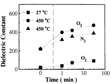
is a suitable process condition for obtaining high dielectric constant and low leakage current.Fig. 7 shows that the dielectric constant of BST deposited at 27°C and 450
"C
and annealed at 650°C in N, and 0,. The dielectric constant of BST films increases with increasing annealing time. The dielectric constant of 450 "C -deposited BST annealed at 650'C in 0, is larger than that of the BST annealed inN,.
Therefore, the polarization or crystallization of BST annealed in 0, ambient is expected to be more enhanced than inN,
ambient. Fig. 8 shows the leakage current of27°C-
and 450°C-deposited BST annealed at 650"C
inN,
and 0,. The leakage current of 0,-annealed BST does not change with annealing time, probably due to the balance of crystallization effect and the reduction of oxygen-vacancy concentration. The leakage current of N,- annealed BST increases slightly with increasing annealing time, because higher crystallization of Npnuealed BST has enhanced the electrons transport and there is no compensation of reduction of oxygen vacancy concentration. The dielectric constant of BST films deposited at 450"C
after annealing in 0,and N, ambient at 650
"C
for 30 min are 476 and 390, respectively. The leakage current density of BST films deposited at 450"C
after annealing in 0,and N, ambient at 650
'
C
for 30 min are 2 . 5 ~ 1 0 - ~ and 1.35x10-' Alcm2, respectively.Fig. 9 shows the leakage current of as-deposited BST films (27°C and 450 "C ). The leakage current at positive bias of BST deposited at 27°C is larger than that of BST deposited at 450"C, because the BST film deposited at 27'C is less dense than at 450
"C
, Fig. 10 depicts the leakage current of BST deposited at 450"C
and annealed at 650"C
in N, and 0, for 3 min. The leakage currents in both conditions have almost the same value. Fig. 11 shows the leakage current of BST deposited at 450°Cunder
650°C annealing in N,180 M. S. TSAI rt ul.
Time
(
min
)
FIGURE 7 The dielectric constant of BST films deposited at 27 "C and 450
"C
as a function of annealing time at 650 "C with 0, andN,
ambient as aparameter.
FIGURE 8 The leakage current of BST films deposited at 27 "C and 450 "C as a function of annealing time at 650 "C with 0, and N, ambient as a parameter.
Electric Field
(
V/cm
)
FIGURE 9 The leakage current of BST films deposited at 27
"C
and 450 "C.Electric Field
(
V/cm
)
FIGURE 10 The leakage current of 450 "C-deposited BST films after annealed for 3 min at 650 "C in 0,
and
N, ambient .182 M. S. TSAI et a1
Electric Field
(
V/cm
)
FIGURE
11 The leakage current of 450 "C-deposited BST films after annealed for 30 min at 650"C
in 0, and N, ambient.
and 0, for 30 min. The leakage current of 0,-annealed BST is smaller than that of N2-annealed BST. Again, 0, ambient is believed to reduce the oxygen vacancies, hence the leakage current of 0,-annealed BST is smaller
than
that of BST annealed in N,.We have also examined the BST films deposited
on
F't bottom electrode at 27"C
and annealed in N,O ambient. The capacitors showed a very large leakage current and therefore their dielectric constant could not be measured. CONCLUSIONSThe dielectric constant and the leakage currnet of 0,- and N,- annealed BST thin films were examined. The post-annealing process can improve the crystallinity of BST films. The dielectric constants of BST films deposited at 450
"C
after annealing in 0, and N, ambient at 650 "C for 30 min are 476 and390, whereas the leakage currents of the films are 2.5x10-' and 1 . 3 5 ~ 1 0 - ~
A/cmz, respectively. The BST films annealed in 0,-ambient have a higher
ELECTRICAL PROPERTIES OF O2 AND N2 183
dielectric constant and a lower leakage current as compared to the films annealed in N,-ambient.
This
may be attributed to the decrease of oxygen vacancies of 0,- annealed BST.References
[l] T. Horikawa, N. Mikami, T. Makita, J. Tanimura, M. Kataoka, K. Sato, and M. Nunoshita, Jpn.
J
Appl. Phys., 33, p. 4126,1993.[2] T. Eimori, Y. Obno, H. Kimura, J. M a t s h s a , S. Kishimura, A. Yoshida, H. Sumitani, T. Maruyama, K. Moriizui, T. Katayama,
M.
Asakura, T.Horikawa, Y. Maruyama, T. Shiano, H. Itoh, K. Sato, K. Namba, T. Nishiimura, S. Satoh and H. Miyoshi, IEDM Tech. Digest, p. 63 1,1993. [3] E. Fujii, Y. Uemoto, S. Hayashi, T. Nasu, Y. shimada, A. Matsuda, M.
kibe,
M. Azuma,T.
Otsuki, G. Kano, M. Scott, L. D. McMillan, and C. A.Paz de Araujo, IEDM Tech. Digest, p. 261, 1992.
[4]