Superior local conductivity in
self-organized nanodots on
indium-tin-oxide films induced by
femtosecond laser pulses
Chih Wang,1Hsuan-I Wang,2Wei-Tsung Tang,2Chih-Wei Luo,2,4 Takayoshi Kobayashi,2,3and Jihperng Leu1,∗
1Department of Materials Science and Engineering, National Chiao Tung University,
Hsinchu, Taiwan
2Department of Electrophysics, National Chiao Tung University, Hsinchu, Taiwan 3Department of Applied Physics and Chemistry and Institute for Laser Science, The
University of Electro-Communications, Chofugaoka 1-5-1, Chofu, Tokyo 182-8585, Japan
Abstract: Large-area surface ripple structures of indium-tin-oxide films, composed of self-organized nanodots, were induced by femtosecond laser pulses, without scanning. The multi-periodic spacing (∼800 nm, ∼400 nm and∼200 nm) was observed in the laser-induced ripple of ITO films. The local conductivity of ITO films is significantly higher, by approximately 30 times, than that of the as-deposited ITO films, due to the formation of these nanodots. Such a significant change can be ascribed to the formation of indium metal-like clusters, which appear as budges of∼ 5 nm height, due to an effective volume increase after breaking the In-O to form In-In bonding. © 2011 Optical Society of America
OCIS codes: (320. 7130) Ultrafast processes in condensed matter, including semiconductors;
(220.4241) Nanostructure fabrication; (190.4400) Nonlinear optics, materials.
References and links
1. M. Al-Ibrahim, H. K. Roth, and S. Sensfuss, “Efficient large-area polymer solar cells on flexible substrates,” Appl. Phys. Lett. 85, 1481–1483 (2004).
2. H. Liu, and R. Sun, “Laminated active matrix organic light-emitting devices,” Appl. Phys. Lett. 92, 063304-1– 063304-3 (2008).
3. H. Kim, C. M. Gilmore, A. Piqu´e, J. S. Horwitz, H. Mattoussi, H. Murata, Z. H. Kafafi, and D. B. Chrisey, “Electrical, optical, and structural properties of indiumtinoxide thin films for organic light-emitting devices,” J. Appl. Phys. 86, 6451–6461 (1999).
4. C. Guill´en and J. Herrero, “Structure optical and electrical properties of indium tin oxide thin films prepared by sputtering at room temperature and annealed in air or nitrogen,” J. Appl. Phys. 101, 073514-1–073514-7 (2007). 5. C. C. Wu, C. I. Wu, J. C. Sturm, and A. Kahn, “Surface modification of indium tin oxide by plasma treatment: an effective method to improve the efficiency, brightness, and reliability of organic light emitting devices,” Appl. Phys. Lett. 70, 1348–1350 (1997).
6. J. K. Sheu, Y. K. Su, G. C. Chi, P. L. Koh, M. J. Jou, C. M. Chang, C. C. Liu, and W. C. Hung, “High-transparency Ni/Au ohmic contact to p-type GaN,” Appl. Phys. Lett. 74, 2340–2342 (1999).
7. R. H. Horng, D. S. Wuu, Y. C. Lien, and W. H. Lan, “Low-resistance and high-transparency Ni/indium tin oxide ohmic contacts to p-type GaN,” Appl. Phys. Lett. 79, 2925–2927 (2001).
8. M. Gross, A. Winnacker, and P. J. Wellmann, “Electrical, optical and morphological properties of nanoparticle indium-tin-oxide layers,” Thin Solid Films 515, 8567–8572 (2007).
9. H. Hosono, M. Kurita, and H. Kawazoe, “Excimer laser crystallization of amorphous indium-tin-oxide thin films and application to fabrication of bragg gratings,” Thin Solid Films 351, 137–140 (1999).
10. G. Legeay, X. Castel, R. Benzerga, and J. Pinel, “Excimer laser beam/ITO interaction: from laser processing to surface reaction,” Phys. Stat. Sol. (C) 5, 3248–3254 (2008).
11. J. G. Lunney, R. R. O’Neill, and K. Schulmeister, “Excimer laser etching of transparent conducting oxides,” Appl. Phys. Lett. 59, 647–649 (1991).
12. H. M. van Driel, J. E. Sipe, and J. F. Young, “Laser-induced periodic surface structures on solids: a universal phenomenon,” Phys. Rev. Lett. 49, 1955–1958 (1982).
13. J. F. Young, J. S. Preston, H. M. van Driel, and J. E. Sipe, “Laser-induced periodic surface structure. II. experi-ments on Ge, Si, Al and brass,” Phys. Rev. B 27, 1155–1172 (1983).
14. B. C. Stuart, M. D. Feit, A. M. Rubenchik, B. W. Shore, and M. D. Perry, “Laser-induced damage in dielectrics with nanosecond to subpicosecond pulses,” Phys. Rev. Lett. 74, 2248–2251 (1995).
15. A. Rousse, C. Rischel, S. Fourmaux, I. Uschmann, S. Sebban, G. Grillon, P. Balcou, E. Frster, J. P. Geindre, P. Audebert, i.e., “Non-thermalmelting in semiconductors measured at femtosecond resolution” Nature 410, 65–68 (2001).
16. J. M. Shieh, Z. H. Chen, B. T. Dai, Y. C. Wang, A. Zaitsev, and C. L. Pan, “Near-infrared femtosecond laser-induced crystallization,” Appl. Phy. Lett. 85, 1232–1234 (2004).
17. C. W. Cheng, W. C. Shen, C. Y. Lin, Y. J. Lee, and J. S. Chen, “Fabrication of micro/nano crystalline ITO structures by femtosecond laser pulses,” Appl. Phys. A 101, 243–248 (2010).
18. M. Huang, F. Zhao, Y. Cheng, N. Xu, and Z. Xu, “Origin of laser-induced near-subwavelength ripples: interfer-ence between surface plasmons and incident laser,” ACS Nano 3, 4062–4070 (2009).
19. Q. Z. Zhao, S. Malzer, and L. J. Wang, “Formation of subwavelength periodic structures on tungsten induced by ultrashort laser pulses,” Opt. Lett. 32, 1932–1935 (2007).
20. X. Jia, T. Q. Jia, Y. Zhang, P. X. Xiong, D. H. Feng, Z. R. Sun, J. R. Qiu, and Z. Z. Xu, “Periodic nanoripples in the surface and subsurface layers in ZnO irradiated by femtosecond laser pulses,” Opt. Lett. 35, 1248–1250 (2010).
21. G. Zhou, P. M. Fauchet, and A. E. Siegman, “Growth of spontaneous periodic surface structures on solids during laser illumination,” Phys. Rev. B 26, 5366–5381 (1982).
22. C. W. Luo, C. C. Lee, C. H. Li, H. C. Shih, Y.-J. Chen, C. C. Hsieh, C. H. Su, W. Y. Tzeng, K. H. Wu, J. Y. Juang, i.e. “Ordered YBCO sub-micron array structures induced by pulsed femtosecond laser irradiation,” Opt. Express 16, 20610–20616 (2008).
23. A. Borowiec and H. K. Haugen, “Subwavelength ripple formation on the surfaces of compound semiconductors irradiated with femtosecond laser pulses,” Appl. Phys. Lett. 82, 4462–4464 (2003).
24. R. L. Harzic, D. D¨orr, D. Sauer, M. Neumeier, M. Epple, H. Zimmermann, and F. Stracke, “Large-area, uniform, high-spatial-frequency ripples generated on silicon using a nanojoule-femtosecond laser at high repetition rate,” Opt. Lett. 36, 229–231 (2011).
25. J. A. Chaney and P. E. Pehrsson, “Work function changes and surface chemistry of oxygen, hydrogen, and carbon on indium tin oxide,” Appl. Surf. Sci. 180, 214–226 (2001).
26. D. Briggs and M. P. Seah, in Practical surface analysis, (John Wiley and Sons, New York, 1993).
27. F. Zhu, C. H. A. Huan, K. Zhang, and A. T. S. Wee, “Investigation of annealing effects on indium tin oxide thin films by electron energy loss spectroscopy,” Thin Solid Films 359, 244–250 (2000).
28. M. Mizuhashi, “Electrical properties of vacuum-deposited indium oxide and indium tin oxide films,” Thin Solid Films 70, 91–100 (1980).
29. S. Noguchi and H. Sakata, “Electrical properties of undoped In2O3films prepared by reactive evaporation,” J. Phys. D: Appl. Phys. 13, 1129–1134 (1980).
30. C. Donley, D. Dunphy, D. Paine, C. Carter, K. Nebesny, P. Lee, D. Alloway, and N. R. Armstrong, “Characteriza-tion of indium-tin oxide interfaces using x-ray photoelectron spectroscopy and redox processes of a chemisorbed probe molecule: effect of surface pretreatment conditions,” Langmuir 18, 450–457 (2002).
31. T. Sz¨or´enyi, L. D. Laude, I. Bert´oti, Z. Kntor, and Zs Geretovszky, “Excimer laser processing of indiumtinoxide films: an optical investigation,” J. Appl. Phys. 78, 6211–6219 (1995).
32. D. R. Lide, in CRC Handbook of Chemistry and Physics, (Taylor and Francis, Boca Raton, Florida, 2003–2004). 33. J. C. C. Fan and J. B. Goodenough, “X-ray photoemission spectroscopy studies of Sn-doped indium-oxide films,”
J. Appl. Phys. 48, 3524–3531 (1977).
34. Y. Shimotsuma, P. G. Kazansky, and J. Qiu, K. Hirao, “Self-organized nanogratings in glass irradiated by ultra-short light pulses,” Phys. Rev. Lett. 91, 247405-1–247405-8 (2003).
35. K. Loeschner, G. Seifert, and A. Heilmann, “Gratinglike nanostructures in polymer films with embedded metal nanoparticles induced by femtosecond laser irradiation,” J. Appl. Phys. 108, 073114–073123 (2010).
36. I. Tanaka, M. Mizuno, and H. Adachi, “Electronic structure of indium oxide using cluster calculations,” Phys. Rev. B 56, 3536–3539 (1997).
1. Introduction
Indium-tin-oxide (ITO) is an important transparent conducting oxide (TCO). ITO films have been widely used as transparent electrodes in optoelectronic devices, such as solar cells [1] and organic light-emitting devices (OLEDs) [2], because of their high electrical conductivity (∼10−4 Ω-cm), coupled with their high transmission (∼90%) in the visible range [3, 4]. In particular, the surface properties of ITO films, such as their electron affinity and work function, also play a key role in establishing the characteristics of OLEDs, owing to their direct contact with the organic materials, as a hole injection layer [4,5]. ITO has also been extensively used as a good ohmic contact material in GaN-base light emitting diodes (LEDs), because ITO shows excellent ohmic behavior in terms of high surface current, which is evidenced by the excellent surface conductivity [6, 7].
In general, a thermal annealing process (≥ 200◦C) is frequently used to change the crys-tallinity of ITO from amorphous (a-ITO) to crystalline (c-ITO), which results in a diminution of resistivity and an increase in transparency [8]. However, this conventional method of thermal annealing at high temperatures does not work for flexible devices, due to their inherently poor thermal stability and the constraint of a low glass transition temperature (Tg), for flexible sub-strates based on plastic materials. To overcome the constraint of avoiding a high-temperature processing step for flexible polymer substrates, therefore, ultraviolet (UV) lasers, such KrF and XeCl excimer lasers with nanosecond pulses, have been reported to anneal ITO films and modify the crystallinity, without a marked rise in the sample temperature [9-11].
Recently, material processing by femtosecond (fs) laser irradiation has attracted a great deal of attention, because a fs pulse of energy can be precisely and rapidly transferred to the film, without thermal effects [12-14]. This is so-called femtosecond laser annealing (FLA). Non-thermal melting in semiconductors, using FLA, exhibits great potential to solve the problem of the thermal budget, in annealing [15, 16]. Pan et al. reported near-infrared femtosecond laser-induced crystallization in amorphous silicon [16]. Very recently, a femtosecond laser was also used to pattern a-ITO films, using the crystallization effect [17]. The high fluences (∼100-1000 mJ/cm2), close to the ablation threshold of a-ITO under a focused fs laser beam, destroyed the a-ITO films, causing many micro-cracks and nanogratings, due to the thermal cycling ef-fect [17]. On the other hand, laser-induced periodic surfaces structures (LIPSS) or ripples, with typical areas of 5μm2to several tens ofμm2, have been observed for various materials, under pulsed laser illumination near their ablation thresholds [18-20]. At present, there are few publi-cations on the modification of ITO films over a large area, using fs laser pulses at low fluence. In addition, the interaction between the fs laser pulses and the ITO film and their impact on the electrical and optical properties are still unclear.
In this study, a large-area (over 200μm×200μm in the center of the beam spot), periodic ripple structure, composed of self-organized nanodots on the surface of ITO films, was induced with low-fluence fs laser pulses (0.1-0.3 mJ/cm2), without scanning. The resistivity, carrier mobility, carrier concentration and especially the surface conductivity of ITO films are signifi-cantly changed, due to the laser induced periodic surface structures (LIPSS), while the optical transmittance is unaffected. The cause of this significant enhancement of the surface electrical properties of the ITO films, with FLA, has been identified via local composition inspection, us-ing Auger electron spectroscopy (AES), and the chemical bondus-ing state analysis, usus-ing X-ray photoelectron spectroscopy (XPS).
2. Experiments
ITO thin films with a thickness of 30 nm and a resistivity of∼4×10⁻²Ω-cm (O2/(Ar+O2) flow ratio is around 0.047) were deposited without optimization on the glass substrates (1 cm×1 cm), by magnetron sputtering deposition at 1000 W power. The ITO target (58 cm×15 cm) was
composed of In2O3with 10 wt% SnO2. After the deposition of ITO films, at room temperature, these samples were then irradiated, using a regenerative, amplified Ti:sapphire laser (Legend USP, Coherent), with 800 nm wavelength, 100 fs pulse duration,∼0.5 mJ pulse energy and 5 kHz repetition rate. The diameter of the laser beam was adjusted to∼14 mm, to ensure full exposure for a sample size of 1 cm×1 cm.
The morphology of the ITO films was examined using a scanning electron microscope (SEM) (HITACHI-S2500 JSM-6500F). The thicknesses of the ITO film, before and after laser pulse irradiation, were determined by surface contour measurement (KOSAKA ET4000A), using a vertical resolution of 0.1 nm. The resistivity, carrier concentration and Hall mobility of the ITO films were measured by Hall measurements, using the Van der Pauw technique (Bio-Rad Microscience HL5500). The refractive index of the ITO film was measured with an n&k Ana-lyzer 1280 (n&k Technology, Inc.). The topography and surface current distribution were fur-ther analyzed using a current sensing-atomic force microscope (CSAFM, Agilent 5500) with a Cr/Pt-coated CSAFM tip (ContE-G type, BudgetSensors, force constant: 0.2 N/m). All CSAFM images reported here were measured with a tip bias of 0.1 V, in a scan area of 10μm×10μm (in the center of 1 cm×1 cm ITO films). The optical transmission measurements were performed using an UV-visible-near-IR spectrophotometer (Shimadzu SolidSpec-3700).
The local compositions of the as-deposited and fs laser irradiated ITO films were examined by Auger electron spectroscopy (AES, ULVAC-PHI 700). Due to the spot size yielded by an integral electron gun of under 5 KeV operating voltage, the data collected by a cylindrical mirror analyzer had a spatial resolution of∼30 nm. The chemical bonding in and composition of the as-deposited and fs laser irradiated ITO films were determined using X-ray photoelectron spectroscopy (XPS, PHI Quantera AES 650), with a monochromatic Al Kα source, at 1486.7 eV. The position of all XPS peaks was calibrated by using the binding energy of 84.0 eV, in Au. For all data in this study, the diameter of analyzed spot was 100μm, for a pass energy of 15 KeV. The peak fitting of the O ls spectra was performed using the Gaussian-Lorentzian function, using an XPS peak fitting program (XPSPEAK4.1 from Dr. R. M. Kwok), and subsequent quantification of the XPS data was obtained by using the peak areas and experimental sensitivity factors. All the O 1s fitted peaks were calculated using 70% Gaussian-30% Lorenztian function and the same full width at half maximum (FWHM).
3. Results and discussion
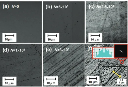
Following normal-incidence irradiation with fs laser pulses, a periodic structure was clearly observed on the surface of ITO films, as shown in the scanning electron microscope (SEM) images of Figs. 1(a-f). Under the same fluence of 0.1 mJ/cm2, the periodic surface structure evolves noticeably, with increasing number of pulses (N). For N = 5×10³ shots [Fig. 1(b)], only few small dots appear on the surface of ITO films. For N≥ 2.5×10⁴shots [Figs. 1(c-f)], however, the laser-induced periodic structure is clearly observed on the surface of ITO films. As shown in the inset of Fig. 1(f), the ripple structure is composed of many sub-micron, in-line dots and the size of the self-organized dots is 20-500 nm. The long axis of the periodic ripple pattern is perpendicular to the direction of the lasers polarization, as represented by the arrow in Fig. 1(f). The laser light is probably scattered and diffracted by the grains, or defects and these scattered waves interfere with each other, to induce the subsequent enhancement of the local-field [21]. Thus, the mixture of the dotted and ripple structures on the surface of ITO films, which is similar to our previous results for ordered YBCO array structures[22], is presumably formed by the solidification of melted dot patterns, under conditions of constructive interference and minimized surface energy.
The spacing of the laser induced periodic surface structures (LIPSS) on the surface of ITO films was estimated by 2D-Fourier transformation, as represented by the red square in Fig. 1(f).
Fig. 1. (a)-(f) show the SEM images of periodic surface structures induced by 800 nm fs laser pulses at a fluence of 0.1 mJ/cm2 and with various pulse numbers (N = 0, 5×10³, 2.5×10⁴, 1×10⁵, 3×10⁵, and 3×10⁶, respectively). The black-square inset shows the en-larged surface features at corresponding locations of (f). The red-square inset shows the 2D Fourier-transformed pattern and its cross-section profile at corresponding locations of (f). The arrow indicates the direction of the laser polarization.
From the positions of satellite peaks, we obtained three kinds of periodicity in the laser-induced ripples, i.e. 798±15 nm, 420±14 nm, and 230±15 nm. For the case of larger ripple spacing with 798±15 nm and 420±14 nm, it can be easily explained by classical scattering model [21]:
Λ= λ
1± sinθ (1)
whereΛis the ripple spacing, λ is the laser wavelength andθ is the incident angle of the laser beam onto the target. However, the shorter ripple spacing of 230±15 nm, which is much smaller than the laser wavelength of 800 nm, cannot be predicted by the classical scattering model with Eq. (1). Thus, due to the scale of ripple spacing with∼200 nm, it may be caused by the second harmonic generation (SHG) with a shorter wavelength of 400 nm around the surface of ITO film. It has been reported that sub-wavelength ripple structures have been observed on the surface of InP, GaP and GaAs semiconductors [23] and Si [24], after fs laser multiple-pulse irradiation in the transparency region. It has been postulated that these nanostructures on the surface of films are induced by the harmonic generation from the near-surface region of films [23, 24]. In our case, the sub-wavelength ripple with∼200 nm was indeed observed in high intensity regions especially in the center of laser Gaussian beam as shown in Fig. 1(f), which implies the high possibility of SHG owing to the surface asymmetry [24]. However, the formation mechanism of this sub-wavelength ripple in ITO films is still unclear. Nevertheless, the effect of self-organized nanodots, near the surface, on the electrical and optical properties and the morphology of self-organized nanodots and their formation will be further examined in the following sections.
function of the number of pulses, from 0 to 3×10⁶shots, at a fluence of 0.1 mJ/cm2. For total shots (N) less than 1000, the carrier concentration of fs laser treated ITO films is almost the same as that of the as-deposited ITO films. Upon further increasing the number of laser shots, to 3×10⁶, the carrier concentration rises noticeably, from∼1×1019cm−3to∼1.6×1019cm−3, and is linearly dependent on the number of shots in the semi-logarithmic plot. In contrast, the carrier mobility is correspondingly reduced, from 12.3 cm2/V-s to 10.2 cm2/V-s, i.e. a 17% reduction, after fs laser irradiation with 3×10⁶shots, at a fluence of 0.1 mJ/cm2. It is believed that the fs laser interference in the reaction duration of each laser pulse is too weak to clearly detect the slight changes in carrier concentration, using the Hall measurement. However, when the accumulated number of pulses exceeds the threshold energy of 1×10³shots, the thickness of the laser-irradiated area becomes thick enough to distinctly show the change in the carrier concentration, using Hall measurement. The resistivity is relatively less sensitive to the number of pulses, showing a 14% reduction (4.3×10⁻² Ω-cm to 3.7×10⁻²Ω-cm), from 0 to 3×10⁶ shots, which can be simply attributed to an increase in carrier concentration.
Fig. 2. The carrier concentration, mobility, and resistivity in the fs laser treated ITO films as a function of the pulse numbers (The solid lines are a guide to the eyes).
The thicknesses of the ITO film before and after irradiation were 30± 1.5 nm and showed no noticeable variation, for repeated surface contour measurement. This strongly implies that the laser fluences used in this study were much less than the ablation threshold energy of ITO films, which is reported to be greater than 100 mJ/cm2[17]. Thus, the effect of thickness on the electrical properties can be eliminated.
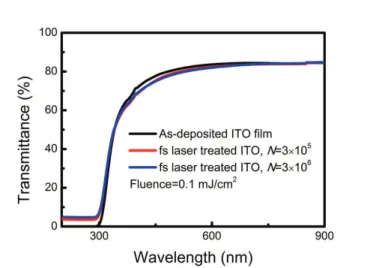
Figure 3 shows the optical transmittance in the as-deposited ITO film and fs laser treated ITO films, for various numbers of shots (N =5×10⁵and 5×10⁶shots), at a fluence of 0.1 mJ/cm2. Compared with an as-deposited ITO film, the optical transmittance of fs laser treated ITO films is about the same, regardless of the number of pulses. Although the electrical properties of the fs laser treated ITO films are noticeably changed, for different number of pulses, N, due to the formation of self-organized nanodots on the surface, the fs laser treated ITO films still maintain their transparency, in the visible to near-infrared (NIR) range. These results indicate that fs laser annealing represents a new way to modify the electrical properties of ITO films, while retaining their high optical transmittance.
The reaction depth of fs laser pulses in ITO films is limited to the top surface, which is unambiguously demonstrated by the current-sensing AFM (CSAFM) measurement. Figures 4(a1-c1) show the topographic images of ITO films, for various numbers of pulses, at a fluence
Fig. 3. The transmittance in the fs laser treated ITO films as a function of wavelengths with various pulse numbers (N = 0, 5×10⁵and 5×10⁶, respectively) at a fluence of 0.1 mJ/cm2.
of 0.1 mJ/cm2, and their corresponding surface current images are illustrated in Figs. 4(a2-c2). For an as-deposited ITO film, the surface roughness is around 0.4 nm [Fig. 4(a1)] and the surface current, for all of the measured area of 10μm× 10μm, is around 0.3 pA in rms (RMS) [Fig. 4(a2)]. After pulsed fs laser irradiation, both the surface roughness [Figs. 4(b1-c1)] and the surface current of ITO films [Figs. 4(b2-c2)] increase, as the number of pulses increases. For N = 3×10⁵shots, the surface roughness is 3.4 nm and the surface current is 7.2 pA in rms (RMS). In addition, some larger dots appear on the surface of the ITO films [Fig. 4(b1)] and many white spots are noted in the surface current image [Fig. 4(b2)].
When the number of pulses is increased to N = 3×10⁶, the dots on the surface of ITO films become larger and even form a regular ripple pattern, with a roughness of 4.2 nm. Meanwhile, the corresponding surface current increases significantly, to 10 pA in rms (RMS), presumably due to the nanodots with high conductivity illustrated in Fig. (c2), which corresponds precisely to the nanodot pattern in the topographic image of Fig. (c1). The height of a bright spot is around 3-5 nm, as shown by the cross-sectional analysis in Fig. 4(d1), and its corresponding current is about 10 pA, as shown in Fig. 4(d2).
In short, the local conductivity of ITO films is remarkably enhanced, i.e. the surface current in the nanodots is∼30 times higher than that of the as-deposited ITO film. However, such a significant reduction in resistivity is not due to the phase transition, because the grazing-incident XRD of fs laser treated ITO films reveals no improvement in the crystallinity. Thus, the composition of the nanodots on the top of the fs laser treated ITO films is further examined in the following section, to determine the cause of the significant increase in the local surface conductivity of the ITO films after femtosecond laser irradiation.
The first derivative (dN/dE) of the AES peaks, including In(MNN), Sn(MNN) and O(KLL) of an deposited ITO film and a fs laser treated ITO film are shown in Fig. 5. For an as-deposited ITO film [bottom-black curve, in Fig. 5(a)], three dN/dE signals can be assigned to the In(MNN) at a kinetic energy of 410 eV [25], Sn(MNN) at a kinetic energy of 433 eV [25,26] and O(KLL) at a kinetic energy of 519 eV [25, 27], respectively. For a fs laser treated ITO film, the dN/dE signals of In(MNN), Sn(MNN) and O(KLL) at point A in Fig. 5(b) are slightly reduced, as compared with the those of an as-deposited ITO film. However, the dN/dE signals at point B in Fig. 5(b) which is located where the dots induced by the fs laser pulses, drop
Fig. 4. (a1)-(c1) The topographic images and (a2)-(c2) their corresponding surface current images of ITO films induced by 800 nm fs laser pulses with various pulse numbers (N = 0, 3×10⁵, and 3×10⁶, respectively) at a fluence of 0.1 mJ/cm2. (d1) Cross-section analysis on the height along the solid line in the AFM image (c1). (d2) Cross-section analysis on the current along the solid line in the CAFM image (c2).
significantly. The reduction in signal is most significant for the dN/dE signal of Sn(MNN). This implies that the composition of ITO films is indeed changed by fs laser annealing, particularly at the positions of the dots.
Based on the disappearance of Sn and the noticeable reduction in In and O, the composition of the self-organized nanodots on the fs laser treated ITO films deviates from the stoichiometry of an as-deposited ITO film. This suggests that the surface of an ITO film irradiated by fs laser pulses changes its composition, from In2O3:SnO2to InOx-like. However, the electrical proper-ties of In2O3, or InOxfilms are inferior to that of ITO films [28, 29]. Further examination of the peak intensities of as-deposited and fs laser treated ITO films reveals that the dN/dE peak in-tensity ratio, for O(KLL) to In(MNN), changed from 1.7 to 1.3(∼23% reduction), after fs laser irradiation. Therefore, the oxygen content may play a key role in inducing such superior local conductivity in the nanodots of fs laser treated ITO films. Additionally, the periodicity of ripple seems to be smeared in high-magnification SEM images due to the ripple is formed by individ-ual dots and too few structures (dots) was included in image as shown in Fig. 5(b). Although the period in high-magnification SEM images is hardly recognized by eyes, the anisotropic 2D Fourier-transformed pattern (the inset of Fig. 5(b)) indicates the intrinsic feature of periodicity
Fig. 5. (a) The first derivative (dN/dE) of AES peaks, In(MNN), Sn(MNN), and O(KLL) as measured for the as-deposited ITO and fs laser treated ITO films. The point A (outside of dot) and point B (inside of dot) correspond to the spots as marked in the SEM top-view image (b) of a fs laser treated ITO film. The red-square inset shows the 2D Fourier-transformed pattern at corresponding locations of (b).
in laser-induced ITO ripples.
The electronic structures of oxides and Indium in fs laser treated ITO films, determined by X-ray photoelectron spectroscopy (XPS) analysis, provides further information on chemical bonding, which may identify the cause of the superior surface conductivity of fs laser treated ITO films.
A schematic representation of as-deposited ITO surface composition, based on Donley’s model [30], is shown in Fig. 6(a). Figures 6(d-g) show the O 1s XPS spectra of fs laser treated ITO films, for various numbers of pulses. For an as-deposited ITO film [Fig. 6(b)], the O 1s XPS spectrum can be fitted by three peaks, which are attributed to the In2O3-like oxygen, at 529.6± 0.1 eV [30,31], oxygen that is adjacent to the oxygen-deficient sites, at 531.0 ± 0.1 eV [30,31], in addition to the hydroxide and/or oxy-hydroxide peak, at 532.0± 0.1 eV [27,30,31]. Compared with a reference sample of In2O3 powder, in Fig. 6(b), the peak for oxygen (at 531.0± 0.1 eV) that is adjacent to the oxygen-deficient sites in an as-deposited ITO film [Fig. 6(c)] increases, owing to the formation of oxygen vacancies, during the thin film sputtering process [27].
It is worth emphasizing that there is a dramatic change in the relative intensities of these three peaks, as the number of pulses increases, in fs laser treated ITO films, which is quantitatively summarized in Table 1. During the FLA process, the oxygen atoms in the In2O3-like sites, adjacent to the oxygen-deficient sites, may be vaporized by the breaking of the In-O (bond strength∼3.31 eV) and Sn-O (5.53 ± 0.13 eV) bonds [32], via possible absorption of multiple photons, especially at the positions of nanodots, due to the higher energy associated with the constructive interference. As N is increased, from 0 to 3×10⁶, the oxygen atoms in the In
2O3 -like sites, adjacent to the oxygen-deficient sites, are significantly reduced, from 80.9% to 47.8%, in the fs laser treated ITO films. These removed oxygen atoms may further form dangling bonds, on the top of the surface, leading to a gradual increase in the intensity of oxygen signals in the OH group, as N increases.
In addition, Fig. 7 shows the XPS spectra of In 3d5/2, for In metals, In2O3powders and fs laser treated ITO films, for various numbers of pulses. For the In metals, the In 3d5/2 peak
Fig. 6. Schematic representation of as-deposited ITO surface composition based on Don-ley’s model [30] (b)The O 1s XPS spectra of In2O3powder and fs laser treated ITO films
with various pulse numbers (N = 0, 5×10³, 2.5×10⁴, 105, 3×10⁵, and 3×10⁶, respec-tively).
Fig. 7. The In 3d5/2XPS spectra of In2O3powder, In metal, and fs laser treated ITO films
with various pulse numbers (N = 0, 5×10³, 2.5×10⁴, 105, 3×10⁵, and 3×10⁶, respec-tively).
Table 1. The relative magnitude of three fitting peaks in XPS O 1s spectra (Fig. 6) for various pulse numbers
The relative magnitude of the fitted peaks in O 1s spectra Samples O in In2O3like site and O in hydroxide and/or
adjacent to deficient site oxy-hydroxide
In2O3powder 85.2% 14.8%
As-deposited ITO film, N=0 80.9% 19.1%
N=5× 10³ 79.5% 20.5%
N=1× 10⁵ 65.0% 35.0%
N=3× 10⁵ 61.5% 39.5%
N=3× 10⁶ 47.8% 52.2%
located at a lower binding energy of 443.7 eV corresponds to the Inobonding state of In-In bonds [27]. For the In2O3powders, however, the In 3d5/2peak located at the higher binding energy of 444.6 eV corresponds to the In3+ bonding state of In2O3 [31, 33]. Hence, the In 3d5/2peak of 444.4 eV for an as-deposited ITO film demonstrates related to the valence states of In2O3. As the number of pulses increases, the In 3d5/2peak gradually shifts, from the In-O bonding state to In-In bonding state. In particular, for N = 3×10⁶, the peak of In 3d
5/2is located at 443.9 eV, which is almost equal to the binding energy of In-In bonds.
This strongly indicates that the appearance of In metal-like clusters in the fs laser treated ITO films, particularly inside the self-organized nanodots, causes the high conductivity in the CSAFM measurements. Similar oxygen deficiencies (SiO2−x) with periodical distribution, have been reported by Shimotsuma et al. [34], for SiO2glass under fs laser irradiation. Recently, Loeschner et al. also demonstrated a related phenomenon in aggregated metal nanoparticles that strongly interact via dipolar forces by using fs laser pluses [35].
Fig. 8. A schematic illustration for the formation of self-organized nanodots induced by the constructive interference of fs laser at near-surface region. The dot is composed of In-rich clusters with height∼5 nm as a result of In-O bonding breaking into In-In under local-field enhancement.
Upon closer inspection of the curve in Fig. 4(d1), it can be observed that the nanodots are bulges in the surface of the ITO films. This can be attributed to the formation of In clusters
with a bond length of 3.82∼ 3.84 ˚A, which is longer than the bond length of In-O (2.12 ∼ 2.21 ˚A) [36], leading to an effective volume increase for the nanodots. If one In-O bond breaks and an In-In bond forms, the increase in the bond length is approximately 72%. The breaking ratio of the In-O bonds in the dots is around 23% based on the AES results. Consequently, we can estimate that the effective increase in the volume of the nanodots, for a 30 nm ITO film, is approximately 5 nm, which is consistent with the roughness results, shown in Fig. 4(d1). To summarize the findings for In clusters and superior local surface conductivity, the formation of self-organized nanodots induced by constructive interference of fs laser, and the size and height of those nanodots are schematically illustrated in Fig. 8 and compared with those for the as-deposited ITO film. This study’s observation of self-organized nanodots with superior local surface conductivity may be of significant interest for applications such as nanolithography, nanophotoelectrons and nanomechanics, in large-area nanotechnology.
4. Conclusion
We report the formation of periodic structures with self-organized nanodots on the surface of ITO films, after fs laser pulse irradiation. This periodic ripple microstructure, which is com-posed of self-organized nanodots, of 20-500 nm size, over an area of 200μm×200μm, can be directly fabricated using single-beam fs laser irradiation, without scanning. The multi-periodic spacing of∼800 nm, ∼400 nm, and ∼200 nm observed in the laser-induced ripple of ITO films can be attributed to the interference between the incident fs laser. The in-line, sub-micron dots are presumably formed by the solidification of melted dot patterns, under conditions of constructive interference and minimized surface energy. After irradiation with fs laser pulses, the electrical properties of ITO films are noticeably modified, e.g. the carrier concentration is increased and the carrier mobility is reduced, while a high optical transmittance is retained. Moreover, the much increased surface current is found to be∼30 times higher than that of as-deposited ITO films, according to CSAFM measurements. From AES and XPS analysis, it is deduced that the self-organized nanodots contain fewer oxygen atoms, i.e. 25%∼30% reduction in the dot regions, owing to the breaking of In-O bonds. In addition, the In 3d5/2XPS spectra results further show that the In-In bonding state gradually appears in the fs laser treated ITO films, as the number of pulses increases. Therefore, the much greater local conductivity in the self-organized nanodots originates from the formation of In metal-like clusters, which, in turn, leads to an effective increase in the volume of the nanodots, with budges of height∼5 nm, for a 30-nm-thick ITO film.
Acknowledgments
The authors would like to thank the support of the National Science Council of Taiwan under Contract Nos.: NSC 100-3113-E-007-002-. The assistance of magnetron sputter by Paragon Technology Corp. is also acknowledged.