the variation immunity of high-performance (super-threshold) and low-voltage (near-/sub-threshold) 6 T SRAM cells is pre-sented. For low-voltage SRAM cells operating at low Vdd, low-Vt design shows smaller variability, while the design tradeoff be-tween performance and leakage should be considered. For high-performance SRAM cells operating at high Vdd, ultra-thin-body SOI SRAM cells with high-Vt design show smaller variability while sacrificing performance compared with the low-Vt de-sign. Our study indicates that hetero-channel SRAM cells enable high-Vt design and exhibit improved Read/Write stability and performance, and maintain comparable RSNM variations for the high-performance SRAM applications.
Index Terms—Hetero-channel, performance, SRAM, variability.
I. INTRODUCTION
H
ETERO-CHANNEL devices using III-V and/or Ge ma-terials [1]–[6] are promising candidates for future CMOS technology due to their high mobility. Their immunity to short-channel effects [1], [2] can be improved by using ultra-thin-body (UTB) device architecture [3]–[5]. Although SRAM cells with III-V channel MOSFETs have been studied and improved performance has been reported [6], [7], the higher leakage and variability may be a concern for III-V channel MOSFETs in SRAM applications.In this paper, threshold voltage (Vt) design and optimization are used to improve the variability of high-performance and low-voltage SRAM cells. For low-voltage (near-/sub-threshold) SRAM cells, [8] shows that the stability and variability of SRAM cells can be improved by using lower Vt devices. However, the impact of Vt design on the variability of high-performance (super-threshold) SRAM cells remains to be ex-amined. In addition, the stability, variability, performance, and cell leakage of III-V-OI and GeOI SRAM cells are analyzed un-der two scenarios (InGaAs-OI(NFET)/GeOI(PFET) and GeOI NFET/PFET) and compared with the SOI SRAM cells. We
Manuscript received July 3, 20112; revised September 21, 2012; accepted November 14, 2012. Date of publication December 7, 2012; date of current version December 19, 2012. This work was supported in part by the National Science Council of Taiwan under Contracts NSC 100-2628-E-009-024-MY2, and in part by the Ministry of Education in Taiwan under ATU Program. The review of this paper was arranged by Editor G. Jeong.
The authors are with the Department of Electronics Engineering and Institute of Electronics, National Chiao Tung University, Hsinchu 30010, Taiwan (e-mail: [email protected]; [email protected]; [email protected]; [email protected]).
Color versions of one or more of the figures in this paper are available online at http://ieeexplore.ieee.org.
Digital Object Identifier 10.1109/TED.2012.2228863
Fig. 1. (a) The schematic of a UTB MOSFET with thin BOX and raised source/drain structure. (b) Ids–Vgscharacteristics of UTB SOI MOSFETs with
high- and low-Vt design.
show that hetero-channel SRAM cells with optimized Vt design exhibit improved stability and performance, and comparable variability compared with the SOI SRAM cells. This paper is organized as follows. Section II describes the device design and simulation methodology used in this work. Section III inves-tigates and compares the impact of Vt design on low-voltage (near-/sub-threshold) and high-performance (super-threshold) SRAM cells. Section IV shows the stability, performance, leakage, and variability of hetero-channel SRAM cells with op-timized Vt design, and the design suggestions for low-voltage and high-performance SRAM cells are provided. Section V concludes the paper.
II. DEVICEDESIGN ANDSIMULATIONMETHODOLOGY
The UTB MOSFETs used in this study have 25 nm gate length (Lg) and raised source/drain structure with thin buried
oxide (BOX) as shown in Fig. 1(a). The device parameters are listed below: channel thickness (Tch) = 5 nm, EOT = 0.7 nm
with high-k gate dielectric (HfO2, permittivity = 22), BOX
thickness (TBOX) = 10 nm, spacer length (Lsp) = 10 nm,
raised source/drain thickness (Tsd) = 22.5 nm, channel doping
concentration (Nch) = 1E16 cm−3, and source/drain doping
concentration (Nsd) = 5.5E19 cm−3for GeOI and 1E20 cm−3
for InGaAs-OI and SOI MOSFETs, respectively.
Fig. 1(b) shows that UTB MOSFETs are designed with two Vt values adjusted by varying the work function [9] to investigate the impact of Vt design on the stability, variabil-ity, performance, and cell leakage of SRAM cells. Band-to-band tunneling [10], [11] and mobility models are calibrated
Fig. 2. ds–Vgs characteristics of UTB SOI MOSFETs with high- and
low-Vt design [9] considering line-edge roughness (LER) at Vds= 1 V. For
LER: correlation length = 20 nm, rms amplitude = 1.5 nm[17]. Note that the threshold voltage variations due to LER are comparable for the high- and low-Vt devices.
Fig. 3. (a) The schematic of a 6 T SRAM cell. (b) The definitions of Read static noise margin (RSNM) and Write static noise margin (WSNM).
with experimental data [5], [12], [13] to accurately assess the power performance of UTB GeOI and InGaAs-OI de-vices using atomistic TCAD mixed-mode simulations [14]. For lightly doped UTB MOSFETs, gate line-edge roughness (LER) is one dominant variation source [15]. To assess the LER, the rough line edge patterns are generated using Fourier synthesis approach [16] with correlation length = 20 nm and rms amplitude = 1.5 nm [17].
III. IMPACT OFVTDESIGN ONLOW-VOLTAGE
(NEAR-/SUB-THRESHOLD)ANDHIGH-PERFORMANCE
(SUPER-THRESHOLD) SRAM CELLS
Device variability caused by continued technology scaling makes diminished static noise margin (SNM) a serious problem for SRAM design. In this section, we show that the Vt design can be used to improve the variability and stability of high-performance and low-voltage SRAMs. Fig. 2 shows Ids–Vgs
characteristics for UTB SOI MOSFETs with high- and low-Vt design adjusted by varying the work function [9]. Notice that the Vt variations (σV t) due to LER are comparable for the high- and low-Vt UTB SOI MOSFETs as shown in Fig. 2.
Fig. 3 shows the schematic of a 6 T SRAM cell and the definitions of Read SNM (RSNM) and Write SNM (WSNM). The RSNM is defined as the minimum noise voltage present at each of the cell storage nodes necessary to flip the state of the cell. Vread,0 is the Read disturb voltage determined by the voltage divider effect between pass-gate and pull-down transis-tors. Vtrip is the voltage needed to flip the cell inverter. Increase
(a) high-Vt and (b) low-Vt design. High-Vt UTB SOI SRAM cells show larger RSNM variation at low Vdd and larger RSNM at high Vdd than the low-Vt UTB SOI SRAM cells.
Fig. 5. High-Vt UTB SOI SRAM cell shows larger RSNM and smaller
σRSNM at high Vdd than the low-Vt one. Low-Vt UTB SOI SRAM cell shows
lower σRSNM and larger WSNM at low Vdd. (μRSNM: mean of RSNM;
σRSNM: standard deviation of RSNM.)
in Vread,0 and decrease in Vtrip will degrade the RSNM. Vwrite,0 is determined by the voltage divider effect between pull-up PFET and pass-gate transistors. Lower Vwrite,0 will benefit the WSNM.
Fig. 4 shows the RSNM variations considering LER for high-Vt and low-Vt UTB SOI SRAM cells. High-Vt and low-Vt SOI MOSFETs with comparable Vt variations (Fig. 2) show different impacts on RSNM variation at high Vdd and low Vdd. Fig. 5 shows that for low-voltage SRAM cell operating at low Vdd, UTB SOI SRAM cell with low-Vt design shows smaller σRSNM, larger μRSNM/σRSNM and larger WSNM than that with high-Vt design. However, for high-performance
Fig. 6. At V dd = 0.4 V, high-Vt UTB SOI SRAM cell shows larger
σVread,0, σVtrip and σRSNM than the low-Vt one.
Fig. 7. At V dd = 1 V, low-Vt UTB SOI SRAM cell shows larger σVtrip and larger Vread,0, therefore, larger σRSNM and smaller RSNM.
SRAM cell operating at high Vdd, UTB SOI SRAM cell with high-Vt design shows larger RSNM, smaller σRSNM and larger μRSNM/σRSNM than that with low-Vt design.
Fig. 6 illustrates why low-voltage SRAM cells (V dd = 0.4 V) show smaller variability with Vt design. For low-voltage SRAM cells operating at low Vdd, low-Vt devices show smaller drain current variation as its operation region moves slightly into the super-threshold region [8]. Therefore, low-voltage SRAM cells with low-Vt design show smaller σVread, 0, σVtrip, and σRSNM than that with high-Vt design.
In Fig. 7, for high-performance SRAM cells operating at high Vdd (V dd = 1 V), SRAM cells with high-Vt design show smaller Vread,0 and larger RSNM than that with low-Vt design because the pass-gate transistor is very sensitive to Vt. At V dd = 1 V, SRAM cells with low-Vt design show larger
σVtrip and σRSNM. As can be seen in Fig. 7 (top figure), the
Vtrip of low-Vt SRAM cells ranges from 0.44 to 0.51 V, while the Vtrip of high-Vt SRAM cells ranges from 0.48 to 0.51 V.
Fig. 8. High-Vt UTB SOI SRAM cell shows lower cell leakage and larger leakage variation than the low-Vt one.
Fig. 9. The “Cell” Read access time degradation of high-Vt UTB SOI SRAM cell becomes smaller as Vdd increases. (64 cells/bit-line)
With balanced N/PFET(same |V t| for N/PFET), NFET is stronger than PFET in the super-threshold region due to more significant contribution of mobility to drain current, while their strength would be comparable in the sub-threshold region. Therefore, under the bias condition for determining Vtrip, low-Vt pull-up and pull-down devices would operate more/ deeper into super-threshold region, resulting in smaller Vtrip tail and larger σVtrip.
Fig. 8 shows that the high-Vt SOI SRAM cells show smaller cell leakage and larger leakage variation at all Vdd than the low-Vt SRAM cells. The OFF current (Ioff) of high-Vt SOI MOSFETs goes more deep into the sub-threshold region com-pared with that of low-Vt SOI MOSFETs. Therefore, the high-Vt SOI MOSFETs exhibit larger Ioff variations than the low-Vt SOI MOSFETs as shown in Fig. 2, and the high-Vt SOI SRAM cells show larger cell leakage variations than the low-Vt SOI SRAM cells.
Fig. 9 shows the “Cell” Read access time comparisons be-tween high- and low-Vt SOI SRAM cells. “Cell” Read access time is analyzed by connecting a column of 64 UTB SOI SRAM cells (64 cells per bit-line). A capacitive load is added onto each bit-line to account for the capacitance of wires and the connected devices. “Cell” Read access time is defined as the time required for developing 0.1 Vdd bit-line differential voltage after the word-line is activated during a Read operation. As can be seen that the high-Vt SOI SRAM cells show larger
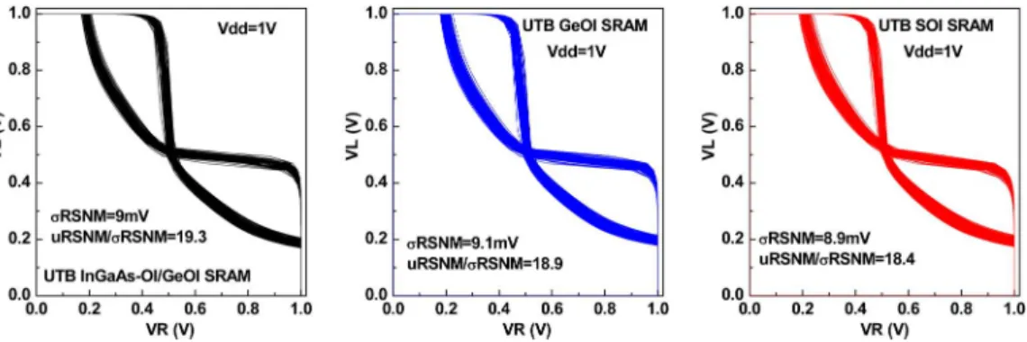
Fig. 10. InGaAs-OI/GeOI SRAM cell shows (a) larger RSNM and (b) larger WSNM than the (same-) high-Vt SOI SRAM cells at high Vdd. (c) Ids–Vgs
characteristics of UTB InGaAs-OI, GeOI, and SOI MOSFETs with same high-Vt design.
“Cell” Read access time than the low-Vt SOI SRAM cells, and the “Cell” Read access time difference between high-Vt and low-Vt SRAM cells becomes smaller as Vdd increases as shown in the inset. The variability of “Cell” Read access time becomes larger as Vdd decreases because the drive current variations are larger in the sub-threshold region than in the super-threshold region. High-Vt UTB SOI SRAM cells show larger “Cell” Read access time variations than the low-Vt UTB SOI SRAM cells. This is because at given Vdd, the drive current variations of high-Vt UTB SOI MOSFETs are larger than that of low-Vt SOI MOSFETs.
Compared with low-Vt design, UTB SOI SRAM cells with high-Vt design show improvement in stability, variability, and cell leakage at high Vdd while sacrificing the “Cell” Read access time. In the following section, we show that the III-V hetero-channel SRAM cells with high-Vt design exhibit signif-icant improvement in “Cell” Read access time compared with the (same-) high-Vt UTB SOI SRAM cells.
IV. InGaAs-OI(NFET)/GeOI(PFET)ANDGeOI SRAM CELLSWITHHIGH-Vt DESIGN
Fig. 10(a) and (b) show that the RSNM and WSNM compar-isons between InGaAs-OI/GeOI SRAM cells and SOI SRAM cells with (same-) high-Vt design. As can be seen, the InGaAs-OI/GeOI SRAM cells show 15% and 18% improvements in RSNM and WSNM at V dd = 1 V, respectively, compared with the high-Vt SOI SRAM cells. The insets of Fig. 10(a) and 10(b) show the improvement in RSNM and WSNM over SOI SRAM cells by using InGaAs-OI/GeOI SRAM cells. Fig. 10(c) shows the Ids-Vgs characteristics of UTB InGaAs-OI, GeOI and SOI
Fig. 11. (a) InGaAs-OI/GeOI SRAM cell shows 48% improvement in Read time than the (same-) high-Vt SOI SRAMs at high Vdd. (b) InGaAs-OI/GeOI SRAM cell shows larger cell leakage than the (same-) high-Vt SOI SRAMs due to band-to-band tunneling.
Fig. 12. InGaAs-OI/GeOI SRAM cell shows larger WSNM, comparable RSNM, smaller Read time, and cell leakage at high Vdd compared with the GeOI SRAM cells.
MOSFETs with same high-Vt design. The InGaAs-OI NFET shows around 80% improvement in Ion compared with the SOI NFET. Therefore, the InGaAs-OI/GeOI SRAM cells have both stronger pass-gate and pull-down NFET devices compared with the SOI SRAM cells. For WSNM, the InGaAs-OI/GeOI SRAM cells with stronger pass-gate NFET device [Fig. 10(c)] show larger WSNM than the SOI SRAM cells at V dd = 1 V. For RSNM, the InGaAs-OI/GeOI SRAM cells with stronger pull-down NFET device [Fig. 10(c)] show smaller Read disturb voltage (Vread,0) and larger RSNM at V dd = 1 V.
Fig. 11(a) shows the “Cell” Read access time comparisons between InGaAs-OI/GeOI and SOI SRAM cells. The “Cell” Read access time is analyzed for 64 cells per bit-line. Read
Fig. 13. InGaAs-OI/GeOI SRAM cell and GeOI SRAM cell with high-Vt design show comparable σRSNM compared with the (same-) high-Vt SOI SRAM. For LER: correlation length = 20 nm, rms amplitude = 1.5 nm [17].
TABLE I
DESIGNSUGGESTION FORLOW-VOLTAGE ANDHIGH-PERFORMANCESRAM CELLS. (↑: IMPROVE,↓: DEGRADE,−: COMPARABLE)
access time depends on the Read current through pass-gate and pull-down transistors. The InGaAs-OI/GeOI SRAM cells with stronger pass-gate and pull-down transistors exhibit 48% improvement in “Cell” Read access time compared with the (same) high-Vt SOI SRAM cells at V dd = 1 V. Due to smaller band-gap, the Ioff of InGaAs-OI and GeOI MOSFETs dom-inated by band-to-band tunneling is larger than that of SOI MOSFETs as shown in Fig. 10(c). Therefore, the cell leakage of InGaAs-OI/GeOI SRAM cells is larger than that of SOI SRAM cells as shown in Fig. 11(b). As Vdd scales from 1 V to 0.4 V, the cell leakage of InGaAs-OI/GeOI SRAM cells shows larger reduction than that of SOI SRAM cells since the band-to-band tunneling leakage is very sensitive to Vdd [18]. The band-to-band tunneling leakage may be reduced by using underlap device design [19], [20]. Fig. 11(b) shows that the InGaAs-OI/GeOI SRAM cells also exhibit smaller cell leakage variations considering LER than the SOI SRAM cells because the cell leakage of InGaAs-OI/GeOI SRAM cells dominated by band-to-band tunneling leakage is less sensitive to LER compared with the sub-threshold leakage [18].
Fig. 12 shows the RSNM, WSNM, “Cell” Read access time and cell leakage comparisons between InGaAs-OI/GeOI SRAMs and GeOI SRAMs with (same-) high-Vt design. (The GeOI PFET is identical for these two scenarios.) Compared with GeOI NFET, InGaAs-OI NFET shows larger drive current (35% improvement) due to its higher mobility as shown in Fig. 12(a) inset. As can be seen, the InGaAs-OI/GeOI SRAM cells with stronger NFET show slightly larger RSNM (+2%), larger WSNM (+16%) and smaller “Cell” Read access time (−21%) at V dd = 1 V. In other words, InGaAs-OI/GeOI SRAM cells with stronger NFET show larger improvement in
WSNM than in RSNM. InGaAs-OI NFET also shows smaller band-to-band tunneling leakage due to its larger band-gap com-pared with the GeOI NFET. Therefore, the InGaAs-OI/GeOI SRAM cells show smaller cell leakage than the GeOI SRAMs as shown in Fig. 12(d).
Fig. 13 shows that the σRSNM of InGaAs-OI/GeOI, GeOI, and SOI SRAM cells with (same-) high-Vt design considering LER at V dd = 1 V. It can be seen that InGaAs-OI/GeOI and GeOI SRAM cells with high-Vt design show comparable
σRSNM compared with the (same-) high-Vt SOI SRAM cells
at V dd = 1 V. In other words, InGaAs-OI/GeOI SRAM cells with high-Vt design improve the stability and performance while maintaining comparable RSNM variations for high-performance SRAM applications. Table I summarizes the de-sign suggestions for low-voltage and high-performance SRAM cells, respectively.
V. CONCLUSION
The stability, variability, performance, and cell leakage of InGaAs-OI/GeOI and GeOI SRAM cells are analyzed and compared with the SOI SRAM cells. For low-voltage SRAM cells, low-Vt design shows smaller variability, larger cell leakage and smaller “Cell” Read access time, and the design tradeoff between performance and leakage should be considered. For high-performance SRAM cells, SOI SRAM cells with high-Vt design show smaller variability and degraded performance. Using InGaAs-OI(NFET)/GeOI(PFET) SRAM cell enables high-Vt design and improves the stability and performance while maintaining comparable RSNM variations for high-performance SRAM applications.
[3] V. P.-H. Hu, Y.-S. Wu, and P. Su, “Investigation of electrostatic integrity for ultra-thin-body Germanium-On-Nothing (GeON) MOSFET,” IEEE
Trans. Nanotechnol., vol. 10, no. 2, pp. 325–330, Mar. 2011.
[4] S. H. Kim, M. Yokoyama, N. Taoka, R. Iida, S. Lee, R. Nakane, Y. Urabe, N. Miyata, T. Yasuda, H. Yamada, N. Fukuhara, M. Hata, M. Takenaka, and S. Takagi, “High performance extremely-thin body III-V-on-insulator MOSFETs on a Si substrate with Ni-InGaAs metal S/D and MOS interface buffer engineering,” in Proc. Symp. VLSI Technol., 2011, pp. 58–59.
[5] L. Hutin, C. Le Royer, J.-F. Damlencourt, J.-M. Hartmann, H. Grampeix, V. Mazzocchi, C. Tabone, B. Previtali, A. Pouydebasque, M. Vinet, and O. Faynot, “GeOI pMOSFETs scaled down to 30-nm gate length with record off-state current,” IEEE Electron Device Lett., vol. 31, no. 3, pp. 234–236, Mar. 2010.
[6] S. Oh and H.-P. Wong, “Viability study of all-III-V SRAM for beyond-22-nm logic circuits,” IEEE Electron Device Lett., vol. 32, no. 7, pp. 877– 879, Jul. 2011.
[7] J.-P. Kulkarni and K. Roy, “Technology circuit co-design for ultra fast InSb quantum well transistors,” IEEE Trans. Electron Device, vol. 55, no. 10, pp. 2537–2545, Oct. 2008.
[8] V. P.-H. Hu, M.-L. Fan, P. Su, and C.-T. Chuang, “Impact of work function design on the stability and performance of ultra-thin-body SOI subthresh-old SRAM,” in Proc. ESSDERC, 2009, pp. 145–148.
[9] J. Petry, G. Boccardi, R. Singanamalla, C. S. Liu, K. Xiong, P. Escanes, J.-L. Huguenin, J. Tseng, L. Van Nimwegen, F. Voogt, C. Bulle-Lieuwma, and M. Muller, “A VFB tunable single metal single dielectric approach using As I/I into TiN/HfO2 for 32 nm node and beyond,” in Proc.
VLSI-TSA, 2009, pp. 57–58.
[10] G. Hellings, G. Eneman, R. Krom, B. De Jaeger, J. Mitard, A. De Keersgieter, T. Hoffmann, M. Meuris, and K. D. Meyer, “Electrical TCAD simulations of a germanium pMOSFET technology,” IEEE Trans.
Electron Devices, vol. 57, no. 10, pp. 2539–2546, Oct. 2010.
[11] V. P.-H. Hu, M.-L. Fan, P. Su, and C.-T. Chuang, “Band-to-band-tunneling leakage suppression for ultra-thin-body GeOI MOSFETs using transis-tor stacking,” IEEE Electron Device Lett., vol. 33, no. 2, pp. 197–199, Feb. 2012.
[12] E. Batail, S. Monfray, C. Tabone, O. Kermarrec, J. F. Damlencourt, P. Gautier, G. Rabille, C. Arvet, N. Loubet, Y. Campidelli, J. M. Hartmann, A. Pouydebasque, V. Delaye, C. Le Royer, G. Ghibaudo, T. Skotnicki, and S. Deleonibus, “Localized ultra-thin GeOI: An innovative approach to germanium channel MOSFETs on bulk Si substrates,” in Proc. IEDM, 2008, pp. 397–400.
[13] M. Poljak, V. Jovanovic, and T. Suligoj, “Features of electron mobility in ultrathin-body InGaAs-on-insulator MOSFETs down to body thickness of 2 nm,” in Proc. IEEE SOI conf., 2011, pp. 1–2.
[14] Synopsys, Inc., Sentaurus TCAD, C2009-06 Manual, Mountain View, CA, 2009.
[15] T. Ohtou, N. Sugii, and T. Hiramoto, “Impact of parameter variations and random dopant fluctuations on short-channel fully depleted SOI MOSFETs with extremely thin BOX,” IEEE Electron Device Lett., vol. 28, no. 8, pp. 740–742, Aug. 2007.
[16] A. Asenov, S. Kaya, and A. R. Brown, “Intrinsic parameter fluctuations in decananometer MOSFETs introduced by gate line edge roughness,” IEEE
Trans. Electron Devices, vol. 50, no. 5, pp. 1254–1260, May 2003.
Vita Pi-Ho Hu (S’09–M’13) received the Ph.D. de-gree from the Department of Electronics Engineering and Institute of Electronics, National Chiao Tung University, Hsinchu, Taiwan, in 2011.
Currently, she is an Assistant Researcher with the National Chiao Tung University.
Ming-Long Fan (S’09) received the B.S. and M.S. degrees from the National Chiao Tung University, Hsinchu, Taiwan, respectively, where he is currently working toward the Ph.D. degree in the Institute of Electronics.
Pin Su (S’98–M’02) received the Ph.D. degree from the Department of Electrical Engineering and Com-puter Sciences, University of California at Berkeley. Currently, he is a Professor at the Department of Electronics Engineering, National Chiao Tung University, Taiwan.
Ching-Te Chuang (S’78–M’82–SM’91–F’94) re-ceived his Ph.D. degree in electrical engineering from the University of California, Berkeley, CA in 1982.
He is currently a chair professor in the Depart-ment of Electronics Engineering, National Chiao-Tung University, Hsinchu, Taiwan.