國
立
交
通
大
學
資訊科學與工程研究所
碩
士
論
文
低 延 遲 非 同 步 直 接 記 憶 體 存 取 控 制 器 之 設 計
Low-Latency Design for Asynchronous DMA Controller
研 究 生:戴俊智
指導教授:陳昌居 教授
低延遲非同步直接記憶體存取控制器之設計
Low-Latency Design for Asynchronous DMA Controller
研 究 生:戴俊智 Student:Chun-Chih Tai
指導教授:陳昌居 Advisor:Chang-Jiu Chen
國 立 交 通 大 學
資 訊 科 學 與 工 程 研 究 所
碩 士 論 文
A ThesisSubmitted to Institute of Computer Science and Engineering College of Computer Science
National Chiao Tung University in partial Fulfillment of the Requirements
for the Degree of Master
in
Computer Science
August 2009
Hsinchu, Taiwan, Republic of China
低延遲非同步直接記憶體存取控制器之設計
學生:戴俊智
指導教授:陳昌居教授
國立交通大學
資訊科學與工程研究所
摘要
現在來說,嵌入式多媒體系統和數位訊號處理器是非常廣泛的被使用到,並且應用 在許多地方。並且由於現在多媒體的影像畫質越來越好,相對的,所需要的資料量也就 伴隨著越來越大。而一般來說,影像處理在一個數位訊號處理器上,常常需要非常大量 的資料量,而這龐大的資料量必須被儲存在外部的記憶體,由於數位訊號處理器的內部 快速記憶體是有限的原因。而處理器直接在外部記憶體處理資料,通常會有不好的效能 影響。所以資料必須從外部記憶體搬運到內部記憶體。因此有效率的從外部記憶體將資 料搬運到內部記憶體,就顯的相對的非常重要。 因此我們提出一個降低直接記憶體存取控制器內的延遲時間的方法,而這個設計方 法就是讓不同通道之間的轉換時間和計算搬運位置的時間平行的同時執行,以降低浪費 的時間,讓整個直接記憶體存取控制器能夠有效率的將資料搬運資料,藉此提升直接記 憶體存取控制器的效能,當用在數位訊號處理器上時,也希望能提升處理器的效能。Low-Latency Design for Asynchronous DMA
Controller
student:Chun-Chih Tai
Advisors:Prof. Chang-Jiu Chen
Department of Computer Science and Information Engineering
National Chiao Tung University
Abstract
Because embedded multimedia systems and digital signal processors are used popularly
and apply many wide range. Because the quality of multimedia image becomes more and
more higher, multimedia image carry enormous amount of data. In general, image processing
on a digital signal processor often requires a lot of image data to be stored in external memory,
because the size of fast internal memory is usually very limited. The efficient data transfer
becomes very important.
We present a method that reduced latency of direct memory access controller. The design
is that digital signal processor processing should be overlapped with direct memory access
controller processing. Therefore, this design reduced 90% the internal latency of direct
Acknowledgement
本論文能夠順利完成,首先要感謝陳昌居老師這兩年來的細心指導,以及口試委員的寶 貴建議,讓我把論文修的夠完整。再來就是要感謝我們實驗室的學長緯民、元騰、宏岳 一開始的建議,並且在寫論文過程中的熱心指導和幫忙,還有我們實驗室的同學嘉承、 榮祥、俊偉的熱心幫助和鼓勵,以及學弟們的加油打氣,感謝大家陪我度過這兩年的研 究所時光。最後還要感謝我女朋友一路的陪伴,並且鼓勵我支持下去,以及家人非常重 要的支持,讓我能專心的把研究所學業完成。Contents
摘要 ...i Abstract...ii Acknowledgement ...iii Contents ...iv List of Figures... vList of Tables ...vii
Chapter 1 Introduction... 1
Chapter 2 Related Works ... 3
2.1 Asynchronous Circuits Design ... 3
2.1.1 Advantages ... 3 2.1.2 Handshaking ... 5 2.1.3 Muller C-element... 9 2.1.4 Asynchronous Pipeline ... 10 2.2 Data Transfers... 12 2.3 AMULET... 13
2.3.1 AMULET3i DMA controller ... 14
2.4 Problem... 16 2.5 Comparison... 17 Chapter 3 Design ... 20 3.1 Data flow ... 20 3.2 Register Formats... 23 3.3 Architecture ... 25 3.3.1 Transfer Engine ... 26 3.3.2 Address Interface ... 29 3.3.3 Counter ... 34 Chapter 4 Simulation ... 38 4.1 Area Simulation ... 38 4.2 Timing Simulation ... 39 Chapter 5 Conclusion ... 44 References ... 45
List of Figures
Figure 1 (a) Bundle data channel... 6
Figure 1 (b) 4-phase protocol ... 6
Figure 2 (a) Dual-rail... 8
Figure 2 (b) Dual-rail protocol ... 8
Figure 3 Transfer diagram ... 9
Figure 4 (a) the symbol of Muller C-element and its gate level... 10
Figure 4 (b) C-element with reset... 10
Figure 5 (a) Four-phase bundle data Muller pipeline. ... 12
Figure 5 (b) Four-phase bundle data Muller pipeline with matching delay. ... 12
Figure 6 DMA controller structure ... 16
Figure 7 (a) Architecture of one interface ... 17
Figure 7 (b) Architecture of two interfaces ... 18
Figure 8 (a) Timeline of one interface ... 19
Figure 8 (b) Timeline of two interface ... 19
Figure 9 Data flow 1... 21
Figure 10 Data flow 2... 22
Figure 11 (a) Source register ... 23
Figure 11 (b) Destination register... 23
Figure 11 (c) Count register... 24
Figure 11 (d) Control register ... 24
Figure 11 (e) Content of the control register ... 24
Figure 12 Architecture ... 25
Figure 13 Transfer Engine ... 27
Figure 14 COMPARE_1... 28
Figure 15 The gate level of Detection ... 28
Figure 16 Engine Register ... 29
Figure 17 Address Interface... 30
Figure 18 (a) DECISION... 31
Figure 18 (b) components of DECISION... 31
Figure 19 SELECT_1 Generator ... 32
Figure 20 SELECT_2 Generator ... 33
Figure 21 MUX ... 34
Figure 22 (a) COUNTER ... 36
Figure 23 (a) The last data of the original architecture ... 40
Figure 23 (b) The first data of the original architecture ... 40
Figure 24 (a) The last data of the improved architecture ... 41
List of Tables
Table 1 Encoding method ... 7
Table 2 the function of Muller C-element ... 9
Table 3 Comparison of data transfers ... 13
Table 4 The improved architecture ... 39
Table 5 The original architecture... 39
Table 6 Comparison of Latency... 42
Chapter 1 Introduction
In recent years, embedded multimedia system and Digital Signal Processor (DSP)
become more and more popular. Because the quality requirement of the images become
higher and higher, the Digital Signal Processor (DSP) needs to handle a lot of information of
the image data. However, most image data are stored in the external memory. That’s because
the size of fast internal memory is usually very limited. Thus, the efficiency of data transfers
of Direct Memory Access (DMA) is becoming one of the most important part of these
embedded multimedia systems [4].
Another important topic is the Direct Memory Access Controller (DMAC). The
processor often uses Direct Memory Access Controller to transfer data and there are many
related research about it. It is widely known that Direct Memory Access transfers has many
advantages, such as eliminating overhead of CPU, increasing processor performance etc. So
we use Direct Memory Access Controller to transfer data for the processor.
It is widely known that low power and solutions are two of the most important issues for
embedded multimedia systems. Asynchronous circuits can easily address these issues [3]. In
order to design the deal embedded multimedia systems with asynchronous circuits, an
different from synchronous circuits design, asynchronous circuits design is an emerging way.
Asynchronous circuits use handshaking protocols rather than the global clock to synchronize
the communication. In addition, the power consumption is lower than synchronous circuits
inherently. That’s because asynchronous circuit have almost zero power dissipation when
there is no work to do. Furthermore, asynchronous circuits design still has other advantages
for circuits, including no clock skew problem, low EMI, and more robustness for environment
Chapter 2 Related Works
2.1 Asynchronous Circuits Design
Asynchronous circuits design is an more emerging circuit design. There are many
differences to traditional circuit designs and the asynchronous circuits. Asynchronous
circuits have lots of advantages and numerous unusual circuit designs.
2.1.1 Advantages
Comparing with synchronous circuits, the asynchronous circuits do not have a
global clock. They use handshaking to complete the communications. As a result of no
global clock, there are lots of advantages in the asynchronous circuits:
z No clock skew: Clock skew is the difference in arrival times of the clock signal at
different parts of the global circuit. Since asynchronous circuits, by definition, have
no global clock, there is no need to worry about clock skew. In contrast, the designer
of a synchronous circuit must often slow down its operation in order to
accommodate the skew.
z Low power requirement: Asynchronous circuits have the potential for very low
hence saving power. These would have been consumed by modules clocked by a
global clock in synchronous circuits while there is no data to process. This is an
increasingly important issue for VLSI, especially since more and more systems are
becoming portable. In fact, the clock power in a synchronous circuit consumes up to
36% to 40% total power [5,6].For these portable systems the advantage of lower
power consumption and simpler power distribution is self-evident: longer battery
life.
z Average case performance: The elasticity of the asynchronous pipeline has led to the
result that the asynchronous pipeline can achieve its processing in the average case
rather than the worst case performance for each stage. When an asynchronous circuit
completes its work, it can transfer data immediately. The asynchronous circuits do
not need to pay attention to other circuits; therefore, the asynchronous circuits do not
need to wait the slowest circuits. On the contrary, the stages of the synchronous
circuits should select execution the time of the critical path to be the clock cycle
time. So the synchronous circuits are worst case performance. But the stages of the
asynchronous circuits are independent. Each stage has its complete time and does
not influence other stages.
z Modularity: Different synchronous designs may have different clock requirements,
On the contrary, the asynchronous designs use handshaking to communicate with
each other. The designers only need to know the inputs, outputs and the way of the
handshaking. The asynchronous circuits can be easily applied to each kind of
circuits, and the designers do not need to take care of the different speed between the
circuits. The modular approach to asynchronous circuits where each modular part
making the whole system is self-timed.
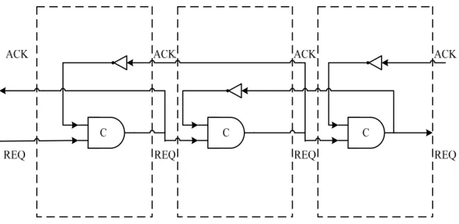
2.1.2 Handshake protocols
Handshaking in the asynchronous circuits have two common protocols: one is
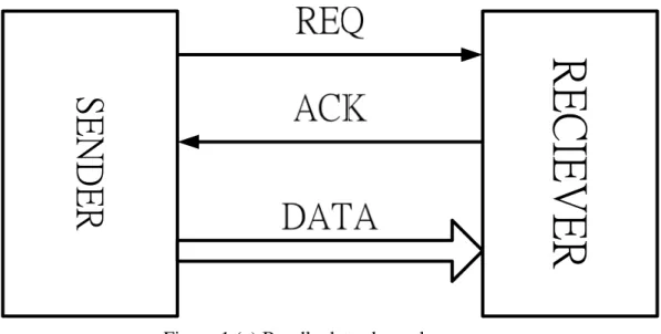
bundle data protocol (Figure 1 (a)), the other is dual-rail protocol (Figure 2 (a)).
Four-phase bundle data has REQ and ACK signals to control all of the transfer steps
(Figure 1 (b)). Initially, REQ and ACK are all 0. When DATA in the Sender is ready,
REQ signal is pulled up to 1 (1), and then the Receiver captures DATA and ACK
signal is pulled up to 1 (2). At the time the Sender receives ACK signal, the Sender
pulls down REQ signal to 0 and stops sending DATA. Finally, the Receiver pulls
SENDER
RECIEVER
Figure 1 (a) Bundle data channel
Figure 1 (b) 4-phase protocol
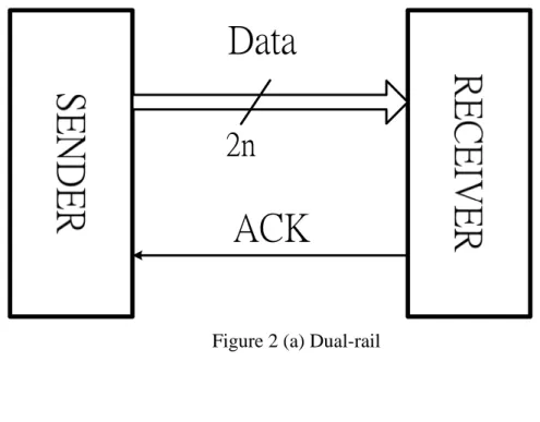
The other way of handshaking is using dual-rail protocol. The special point of
dual-rail is that the system does not have REQ signal, and use 2-bits to encode 1-bit
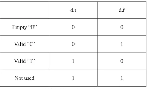
data. The encoding method is shown in Table 1. It use 00 to show that there is no
data (EMPTY), use 01 to encode the data of 0 (VALID) and use 10 to encode the
data of 1 (VALID). If the system use dual-rail protocol to transfer n-bits data, there
d.t d.f
Empty “E” 0 0
Valid “0” 0 1
Valid “1” 1 0
Not used 1 1
Table 1 Encoding method
Because of the system does not have REQ signal, the RECEIVER needs extra
circuits to detect the arrival of the DATA signals. This special design in dual-rail
system is called complete detection.
Figure 2 (b) shows the process of data transfer using dual-rail protocol. Initially,
DATA is EMPTY (all 0), and ACK signal is 0. When DATA is valid and the
RECEIVER detects that DATA is ready, the RECEIVER captures DATA and pulls
up ACK signal to 1. Then the SENDER stops sending DATA, so DATA becomes
EMPTY. Finally, the RECEIVER pulls down ACK signal to 0 and the transfer is
2n
ACK
Data
Figure 2 (a) Dual-rail
Figure 2 (b) Dual-rail protocol
Valid DATA will appears separately. Dual-rail protocol uses EMPTY to
separate each DATA. When the SENDER sends one time of DATA, the data wires
will return to EMPTY. So the sequence of DATA is EMPTY – VALID – EMPTY –
Figure 3 Transfer diagram
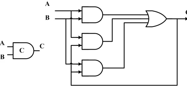
2.1.3 Muller C-element
Muller C-element is a fundamental component in asynchronous circuit design.
It is a state-holding element just like an asynchronous set-reset latch. The function
of Muller C-element is shown in Table 2. When both inputs are logic 1, the output is
logic 1. When both inputs are logic 0, the output is logic 0. Otherwise, the output
does not change. Figure 4 (a) shows the symbol of Muller C-element and its gate
level implementation. It uses three AND gates and one OR gate. The output C will
return to the input and become one of the inputs. Figure 4 (b) shows the C-element
with reset signal.
Input 1 Input 2 Output
0 0 0
0 1 No change
1 0 No change
1 1 1 Table 2 the function of Muller C-element
Figure 4 (a) the symbol of Muller C-element and its gate level
A
B
C
reset
Figure 4 (b) C-element with reset
2.1.4 Asynchronous Pipeline
There are several asynchronous pipeline implementation styles have been
four-phase bundled data protocol [1]. It is implemented with C-elements and
inverters. Another important model is called micropipeline which uses two-phase
bundled data protocol, introduced by Ivan Sutherland in his Turing Award Lecture
[1]. Other asynchronous pipeline implementations use different circuits design
methods to replace the C-elements and latches. Because of the model we choose, we
will introduce the Muller pipeline.
Figure 5 (a) shows a four-phase bundled data pipeline which based on the
Muller pipeline. A Muller pipeline is used to generate local clock pulses. The clock
pulse generated in one stage with the pulses generated in the neighboring stages in a
carefully controlled manner. Figure 5 (a) shows a pipeline without data processing.
If a pipeline with data processing, the combinational circuits can be added between
the stages. In order to maintain correct behaviors matching delays have to be
inserted in the request signal paths. Figure 5 (b) shows a pipeline with data
Figure 5 (a) Four-phase bundle data Muller pipeline. C C C REQ ACK
REQ REQ REQ ACK ACK ACK Matching delay Matching delay
Figure 5 (b) Four-phase bundle data Muller pipeline with matching delay.
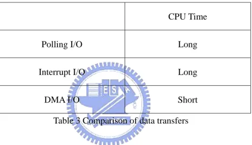
2.2 Data Transfers
This section describes three ways of data transfers: program controller I/O (polling
I/O), interrupt I/O and DMA I/O. The program controller I/O lets I/O devices
The cycle checking of CPU gets information of data and CPU starts to service. When
I/O devices need to transfer, the interrupt I/O uses the interrupt signal to request CPU that
starts to transfer by its order of priority. The DMA I/O uses device controller to transfer
directly between I/O devices and memory without CPU. Table 3 shows comparisons with
program controller, interrupt and DMA.
CPU Time
Polling I/O Long
Interrupt I/O Long
DMA I/O Short
Table 3 Comparison of data transfers
2.3 AMULET
This section introduces a series of the AMULET processors that contain the
AMULET1, the AMULET2e, the AMULET3i.
z AMULET1 [7]: The AMULET1 was presented in 1994. It is a test piece
demonstrating feasibility of a full custom asynchronous processor that is designed
with Sutherland’s two-phase micropipelined method. AMULET1 is just a
between on chip and off chip. AMULET1 is the ARM6 compatible processor.
z AMULET2e [8]: The AMULET2e was presented in 1996. It is an embedded
microprocessor with memory, cache, peripherals and AMULET2 core. AMULET2e
is designed with four-phase protocol. AMULET2e is the ARM7 compatible
processor.
z AMULET3i [9]: The AMULET3i was presented in 2000. It contains AMULE3 core
and other asynchronous marcocell. The AMULET3i marcocell consists of a number
of components and connected together by a marcocell bus called MARBLE BUS.
These components contain RAM, DMA controller and etc. AMULET3i is the ARM9
compatible processor.
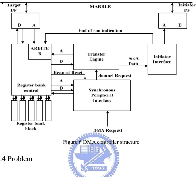
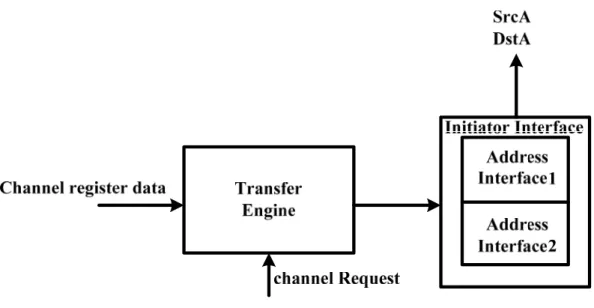
2.3.1 AMULET3i DMA controller
The AMULET3i DMA controller is used primarily to transfer data between on chip
and off chip [2]. The DMA controller (Figure 6) contains: Register bank control,
ARBITER, Synchronous Peripheral Interface (SPI), Transfer Engine and Initiator
Interface. The Register bank control is used to perform the operations of the register bank
block. The ARBITER is used to decide the data that comes from the transfer engine or the
MARBLE bus. The data should be stored into the register bank block. The Synchronous
Peripheral Interface (SPI) is used to control the mapping of these incoming synchronous
channels. The SPI contains not only the channel mapping hardware but also request state
machines for each channel. The Transfer Engine is used to receive requests that come
from the SPI and the channel register values and sent them to the Initiator Interface. The
Transfer Engine has a main companion process: the Initiator Interface. The Initiator
Interface is used to actually perform the DMA transfer operation and also signals
end-of-transfer to register bank for finishing updating register bank registers. A DMA
transfer begins with DMA request arriving on SPI. The operations of a transfer should be
performed as follows. First, the SPI receives DMA request and maps it onto DMA
controller channel. Then, the Transfer Engine receives channel request and requests a
copy of the register contents for requesting channel from register bank control. After that
the initiator interface receives the channel register values from the transfer engine and
sends the source address and destination address to the initiator I/F for finishing transfers.
When the transfer would actually have been completed, the end-of-transfer signal to
register bank control and the channel register values of the register bank control should
Figure 6 DMA controller structure
2.4 Problem
The AMULET3i DMA controller allows only a certain number of transfers that
should be performed for each DMA transfer. Due to the image processing of today’s
Digital Signal Processor often requires a lot of image data and the size of fast on chip
memory is very limited, a lot of image data are stored in external memory. As frequency
and processing of DSP are increasing, the data rate fully utilize the available processing
bandwidth. In terms of results of experiment [10], the same data is transferred. The small
data size transfer can have perfect contrast efficiency with the general (large) data size
transfer. Due to all of the above, the AMULET3i DMA controller could produce longer
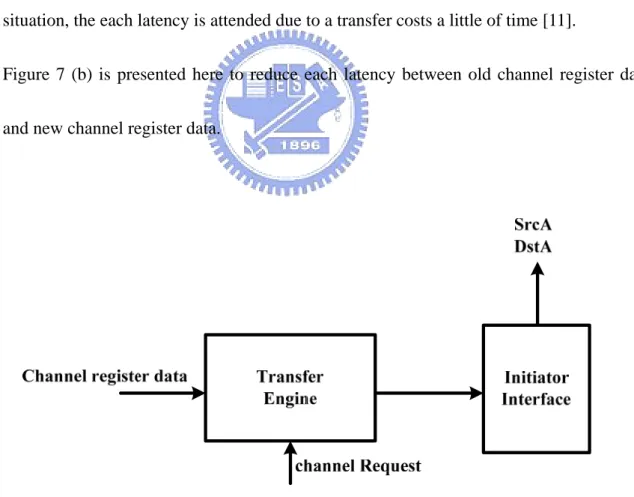
2.5 Comparison
Figure 7 (a) shows the channel register data is sent to the initiator interface from the
transfer engine. When the next channel register data will be sent to the initiator interface,
the current channel register data is completed in the initiator interface. So, the each
latency is produced between old channel register data and new channel register data from
the transfer engine to the initiator interface. In the general size data situation, the each
latency is ignored due to a transfer costs amount of time. But in the small size data
situation, the each latency is attended due to a transfer costs a little of time [11].
Figure 7 (b) is presented here to reduce each latency between old channel register data
and new channel register data.
Figure 7 (b) Architecture of two interfaces
Figure 8 (a) show the original DMA controller that the transfer engine requests three
times copies of the register contents and sends to the initiator interface. Every different
data has a setup time of the data of the initiator interface. Figure 8 (b) shows our new
DMA controller that contains two initiator interfaces. The first data has a setup time of
the data of the initiator interface. The setup time of the other data are overlapped. The
setup Time and DMA transfer time are overlapped. Therefore the latency between the
Figure 8 (a) Timeline of one interface
Chapter 3 Design
In previous chapter, we have compared advantages and disadvantages of asynchronous
circuits. In addition, we also describe ways of data transfer between external memory and
internal memory. We have described benefits of data transfer using AMULET3i Direct
Memory Access Controller for the processor in previous section. But there are still some
points that can be improved in lots of small size data and transfers in many times condition.
This chapter will describe with the architecture first, and it then talks about the overall
operation. Depending on the proposed architecture, the data transfer flow and data formats to
meet the requirements will be discussed. Finally, we will describe the design architecture in
detailed.
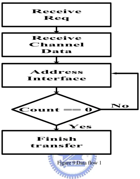
3.1 Data flow
The data flow have two parts: one is used in the overall design and the other is
used in Address_Interface of the design. The first part is shown in Figure 9. This flow
shows how to transfer the data in the overall design. The design receives the value of
channels from register bank block as input and decides the Counter that whether
Figure 9 Data flow 1
First, the request signal is sent to the DMA controller. If the request is arrival, the
Transfer Engine receives the data of channels. The Address_Interface receives the data from
the Transfer Engine. The Counter receives the data from the Address_Interface and computes
addresses. When the Count state of the Counter is “Yes” which indicates data transfer of the
channel should be finished. Otherwise, the Count state of the Counter is “No” which indicates
data transfer of the channel should continue transferring.
The other data flow shows how the data can be stored in the Address_Interface from the
Figure 10 Data flow 2
The data is sent by the Transfer Engine. First, The Address_Interface checks the Interface
is Empty or not. If the Interface is full with 1 symbol, the data cannot be stored into the
Interface. Otherwise, the data can be stored into the Interface. According to the state of the
Interface, the data is stored into one of two Interfaces. The 00 and 10 symbols indicate that the
data is stored into the Interface1 and the 01 symbol indicates that the data is stored into the
3.2 Register Formats
This paragraph describes that how we design register formats within a channel.
These register formats are transmitted from the register bank block. These register
formats how to be designed in the overall design.
The value of each channel contains four registers: SOURCE Address register,
DESTINATION Address register, COUNT register and CONTROL register. The
SOURCE register stores 32-bit source addresses for transfers, and the DESTINATION
register stores 32-bit destination addresses for transfers. The COUNT register stores
32-bit count of remaining transfers to perform. The transfer will be terminated when the
COUNT register is decremented to zero. The CONTROL register specifies the updates to
be performed on the other three registers and which this channel is connected.
Figure 11 (a) Source register
Figure 11 (c) Count register
Figure 11 (d) Control register
Figure 11 (e) Content of the control register
The CONTROL register has 3 fields: Channel_No, DRQ and Enable. If the Enable
bit is set, this channel should be considered for transfers when a new DMA request
arrives. When transfers of channel finish, the Enable bit should be reset to indicate that
this channel can receive a new DMA request. The DRQ bit indicate the initial state for the
request. If the DRQ bit is set, it means that the data have arrived really. Resetting the
DRQ bit specifies that request from corresponding channel data should trigger a transfer.
The Channel_No bits indicates which channel numbers receive the source and destination
3.3 Architecture
The architecture consists of three major constructions: Transfer Engine,
Address_Interface, Counter (Figure 12).
Figure 12 Architecture
The three parts have different functions: Transfer Engine is used to receiving the
values of channels, Address_Interface is used for sending the value of channels out and
Counter computes the value from Address_Interface. This architecture has two ports
which can receive the value of channels from register bank block, and it has one port to
send source address and destination address out to the bus. In general, the input speed is
faster than the output speed; Counter can compute next address and sent next address out
if current address transfer finishes. In addition, Counter can compute next address and
Initially, the design needs to confirm if the request signal arrives or not. If the
request signal is arrival, it will start to receive the values of channels. This work is done
in Transfer Engine.
First, the Transfer Engine receives the value of channels and sends the value of a
channel out to Address_Interface. The Address_Interface contains Interface_1 and
Interface_2, and the value are stored in empty the Interface. The Address_Interface sends
the value out to Counter, and the Transfer Engine send the value out to the
Address_Interface simultaneously. When the current channel finishes, the
Address_Interface sends the next value of the channel out to Counter immediately. These
will operate in our DMA controller design according to the above method.
3.3.1 Transfer Engine
Transfer Engine (Figure 13) has one input ports: Channel_Data_in and one output
port: Engine_Data_out. The Channel_Data_in is stored in the data of channels from
register bank block in AMULET3i DMA Controller architecture. First, Transfer Engine
receives the value of channels and stores it in the Engine Register. These should be
controlled by the control signal of the COMPARE_1. When the data of the Engine
Figure 13 Transfer Engine
The COMPARE_1 (Figure 14) is used to receive count that should be stored in the
Engine Register and ACK signal. The COMPARE_1 also decides the Channel_Data to
be stored into the Engine Registers or to reset the data of the Engine Register by the
control signal of the COMPARE_1. First, the Engine Register_count and ACK signal are
operated by the COMPARE_1 and produce COMPARE_1 control signal. When symbol
of COMPARE_1 is 0, the Channel_Data can be stored into the Engine Register. When
symbol of COMPARE_1 is 1, the Channel_Data cannot be stored into the Engine
Register and reset the data of the Engine Register. Figure 15 shows the gate-level
Figure 14 COMPARE_1
Figure 15 The gate level of Detection
The Engine Register (Figure 16) receives the Channel Data_in and COMPARE_1
control signal. When the control signal is 0 controlled by COMPARE_1 signal, four
MUX select the source_address, destination_address, count, and Ctrl separately and store
these data into four registers. On the other hand, and the signal is 1 controlled by
Figure 16 Engine Register
3.3.2 Address Interface
Address Interface (Figure 17) has two input ports: Counter_Data and Engine_Data and
one output port: Interface_Data. The Counter_Data comes from the COUNTER after
Interface_Data is computed every time. The Engine_Data from Transfer Engine are stored in
registers. The Interface_Data is sent out to the COUNTER and the COUNTER computes
source address, destination address and count. The SELECT_1 and SELECT_2 signal are
used to store the data. The SELECT_2 signals that is used to control MUX. The MUX is used
to decide which one of data of two Interfaces can be sent out.
Figure 17 Address Interface
By method of judgment of SELECT_1 and SELECT_2. The DECISION (Figure 18 (a))
is used to decide the Counter_Data that should be stored into which one of two Interfaces. It is
also used to decide Engine_Data that should be stored into which one of two Interfaces.The
Counter_Data and Engine_Data cannot be stored the same interface simultaneously. Figure 18
(b) shows components of the DECISION that contains two DEMUX and two MUX. The
DEMUX_1 decides Counter_Data that should be sent to the MUX_1 or the MUX_2. The
DEMUX_2 decides Engine_Data that should be sent to the MUX_1 or the MUX_2. The
MUX_1 decides the one of two data that should be sent to the Interface_1. The MUX_2
Figure 18 (a) DECISION
The SELECT_1 Generator (Figure 19) is used to receive count that should be stored in
two Interfaces. It also decides the Engine_Data that should be stored into which one of two
Interfaces or can not store into the Interfaces by SELECT_1[1:0] signal. First,
Interface1_count and Interface2_count are operated by the Detection and produce SELECT_1
[1:0] signal. If the SELECT_1 [1:0] signal is 00 or 10, the Engine_Data should be stored into
the Interface_1. When the SELECT_1 [1:0] signal is 01, the Engine_Data can be stored into
the Interface_2. But the SELECT_1 [1:0] signal is 11, the Engine_Data can not be stored into
both of the Interface_1 and the Interface_2.
Figure 19 SELECT_1 Generator
The SELECT_2 Generator (Figure 20) is used to receive the SELECT_1[1:0]
signal and Comp_Dect signal that comes from the COUNTER. The SELECT_2 signal
SELECT_2 signal. The Interface_Data is updated from the COUNTER. The
SELECT_2 signal also decides to select which one of the data of two Interfaces that
should be sent out. Initially, the SELECT_2 signal and Comp_Dect signal are 0. When
the Comp_Dect signal becomes 1, the SELECT_2 signal becomes 1 from 0 and later
the Comp_Dect signal becomes 0 from 1. When the Comp_Dect signal becomes 1
again, the SELECT_2 signal becomes 0 from 1 and later the Comp_Dect signal
becomes 0 from 1. So, the SELECT_2 signal changes 0 Æ 1 Æ 0 Æ 1, when the
Comp_Dect signal becomes 1.
The MUX (Figure 21 MUX) is used to receive Interface1_Data and Interface2_Data. The
MUX decides which one can be sent out to the COUNTER depending on the control signal
SELECT_2..
M
U
X
SELECT_2
Interface1_Data
Interface2_Data
Interface_Data
Figure 21 MUX3.3.3 Counter
The COUNTER (Figure 22 (a)) is used to receive Interface_Data and ACK signal.
The COUNTER contains the counter to compute Interface_Data. The counter (Figure 22
source address, destination address and count. The counter produces Counter_Data. The
Counter_Data contains source address, destination address and count. The source address
indicates the source of a data transfer, the destination address indicates the destination of
a data transfer and the count indicates the number of times of data transfers. When a data
transfer finishes and the counter accept the ACK signal is 1, the source address and the
destination address are incremented by 4 and the count is decremented by 1. Figure 22 (c)
shows how to produce the Comp_Dect signal by Count and Ctrl of the Interface_Data.
The initial the Comp_Dect signal is 0. The count is equal to 0 if the transfer is finished.
The DRQ bit is is equal to 1 if the data arrives. When the count is 0 and the DRQ bit is 1,
the Comp_Dect signal becomes 1. If the Comp_Dect signal is 1, it indicates that current
transfer is finished. Then, when the next Interface_Data arrives and starts the new data
Figure 22 (a) COUNTER
Chapter 4 Simulation
In chapter 3, we have described the proposed design of function block in detail. We use
the Verilog HDL to build all of the components and construct the whole architecture with
above mentioned our sub-modules described in chapter 3.
We implemented our improved section of asynchronous DMA controller in gate-level.
The design was synthesized and simulated with the TSMC 0.13um library and the simulator is
ModelSim 6.0. The experimental group of our design is the new proposed architecture, and
the control group is the original Amulet3i DMA controller. We also compare our new DMAC
design with the original design of Amulet3i.
4.1 Area Simulation
The areas of each sub-modules are shown in Table 4. We can discover that the area of the
Address Interface is largest. This is because the Address Interface contains complicated
control signals and elements. The area of Transfer Engine is 3119.8 um2, the area of Address
Interface is 8261.2 um2 and the area of Counter is 6996.7 um2. The total area is 18501.7 um2.
Module Area(um2)
Transfer Engine 3119.8
Address Interface 8261.2
Counter 6996.7
Total 18501.7
Table 4 The improved architecture
Module Area(um2)
Transfer Engine 3119.8
Address Interface 2909.4
Counter 6908.4
Total 13054.7
Table 5 The original architecture
4.2 Timing Simulation
In this section, we have two simulation results: one is original architecture and the other
is our new architecture. The Figure 23 (a) shows the timing of the last data of the channel 1
with original architecture. Figure 23 (b) shows the timing of the first data of the channel 2
with original architecture. The Figure 24 (a) shows the timing of the last data of the channel 1
with the new architecture. Figure 24 (b) shows the timing of the first data of the channel 2
Figure 23 (a) The last data of the original architecture
Figure 24 (a) The last data of the improved architecture
Table 6 shows the latency comparison of original and new architecture. The latency means the
time between last data of current channel and first data of next channel. The result represents
new latency is less than original latency that the new architecture can reduce latency between
the different channels. Table 7 shows the comparison of ratio of latency in different count
conditions. The original time represents the time of data transfer of original initiator interface.
The new time represents the time of data transfer of new initiator interface. Because the new
design circuit is more complicated than the original design circuit, the new time is much
bigger than the original time from table 7. When the count is 5, the improvement is 9%. When
the count is 10, the improvement is 4.5%. When the count is 15, the improvement is 3%.
Therefore, the count much smaller and the improvement latency is more obvious.
Latency(ps)
Original 1026
New 104
Count = 5 Count = 10 Count = 15
Original Time(ps) 10075 20150 30225
Original Latency(ps) 1026(10%) 1026(5%) 1026(3.3%)
New Time(ps) 10570 21140 31710
New Latency(ps) 104(1%) 104(0.5%) 104(0.33%)
Chapter 5 Conclusion
Because the performance of DMA data transfer is the bottleneck of the multimedia
application performance, it’s important to improve the performance of DMA controller. In this
thesis, we propose an improved DMA controller of Amulet3i ones to reduce the latency of
DMA data transfer. We use this new proposed architecture to reduce the latency between the
transfer engine and the address interface with the different channels. We use asynchronous
circuits design to solve the problem of global clock.
We propose new architecture should be applied in asynchronous Digital Signal Processor.
The new latency reduced 90% than the original latency. In chapter 4, we can find this new
architecture has perfect performance in lots of smaller data size transfer condition. Due to
DSP processing should be overlapped with DMA processing, the new proposed architecture
and data size format use together not only have lower latency but also have better
performance. Especially, a sequence of small size data is transferred, the new improvement
References
[1] Jens SparsØ and Steve Furber,“Principles of Asynchronous Circuit Design”, London, 2001
[2] Andrew Bardsley, “Implementing Balsa Handshake Circuits”, Ph.D thesis, Department of
Computer Science, The University of Manchester, 2000
[3] F. Aghdasi and A. Bhasin, “DMA controller design using self-Clocked methodology”,
IEEE AFRICON, vol. 1 and 2, pp443-450, 2004
[4] Kim D., Managuli R. and Kim Y., “Data Cache and Direct Memory Access in
Programming MediaProcessors”, IEEE MICRO, vol. 21, pp. 33-42, 2001
[5] R. Y. Chen, M. Vijaykrishman and M. J. Irwin, “Clock Power Issues in System-on-a-Chip
Designs”, IEEE International Computer Society Workshop on VLSI, pp.48-53, 1999
[6] David Duarte, Vijaykrishman Narayanan and Mary Jane Irwin, “Impact of Technology
Scaling in the Clock System Power”, IEEE International Computer Society Annual
Symposium on VLSI, pp.59-64, 2002
[7] N.C. Paver, “The Design and Implementation of an Asynchronous Mircoprocessor”, Ph.D
thesis, Department of Computer Science, The University of Manchester, 1994
[8] S.B. Furber, P. Day, J.D. Garside, S. Temple, P. Day, J. Lin and N.C. Paver, “AMULET2e:
An Asynchronous Embedded Controller”, In the third International Symposium on
[9] J.D. Garside, S.B. Furber and S.H. Chung, “AMULET3 Revealed” , in the third
International Symposium on Advanced Research in Asynchronous Circuits and Systems,
ASYNC97, Department of Computer Science, pp.51-59, 1999
[10] D. Comisky, S. Agarwala and C. Fuoco, “A Scalable High-Performance DMA
Architecture for DSP Applications”, IEEE International Conference on Computer Design:
VLSI in Computers and Processors, pp.414-419 , 2000
[11] Zinner C. and Kubinger W., “ROS-DMA: A DMA Double Buffering Method for
Embedded Image Processing with Resource Optimized Slicing”, Proceedings of 12th
IEEE Real-Time and Embedded Technology and Applications Symposium, pp.361-372,