A Single-Chip Low-Power Tunable CMOS Low-IF Single-Conversion ISM Receiver
*Chia-Pei Chen, Simon C. Li, *Hong-Sing Kao, **Chung-Chih Su and *Kuei-Ann Wen
*Institute of Electronics, National Chiao-Tung University, HsiuChu, Taiwan
Advanced Technology & Integrated System Laboratory (ATIS Lab.), National Yunlin University of Science and Technology ** AlfaPlus Semiconductor Inc., HsinChu, Taiwan
Abstract—A single-chip tunable CMOS low-IF single-conversion receiver operated in the 915-MHz ISM band is proposed. A new 10.7-MHz IF section including a limiting amplifier and FM/FSK demodulator is employed. Near IF section sensitivity of –72 dBm, the demodulation constant of FM/FSK demodulator is 15 mV/kHz and the dynamic range of the limiting amplifier reaches 80dB. With on-chip tunable components in low power LNA and LC-tank VCO circuit, the receiver measures a RF gain of 15dB at 915-MHz, sensitivity of –80dBm at 0.1% BER, IIP3 of –9dBm, and NF of 5dB with current consumption of 33mA and a chip area of 6 mm2.
1.
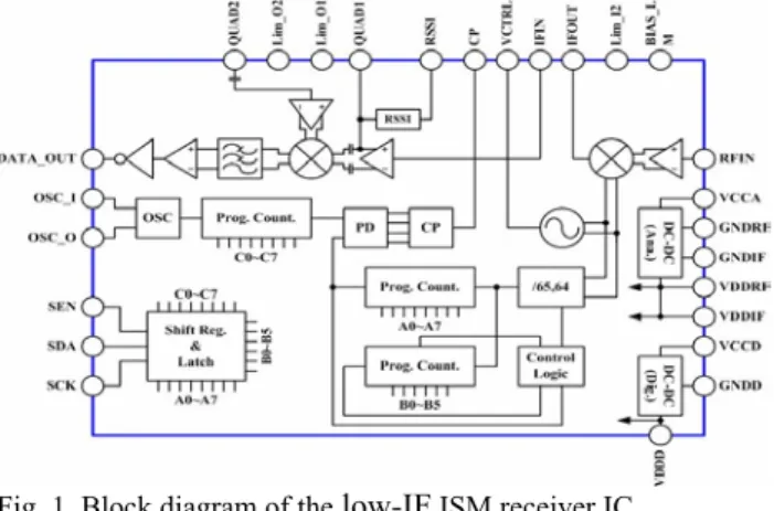
IntroductionThe demand for low-cost wireless systems has soared in the recent past. There is a rapidly growing market for low power short-range wireless systems for alarm systems, sensors, and controls. Because of their limited range and low data rates, these short-range systems often operate in the ISM bands. There is a tradeoff among antenna size, power consumption, and design feasibility that depends on the frequency of operation. The 915-MHz ISM band was selected for this work as a compromise among these parameters. To meet such demand, much work has been focused on realizing fully integrated receiver (Rx) within CMOS technologies [1]-[3]. In this paper, a fully integrated wireless receiver IC is intended for use in the unlicensed 902-928 MHz ISM band as part of a system that communicates at rates between 2kbps to 390kbps. The single–chip receiver IC contains a low-noise amplifier, a mixer, a frequency synthesizer and a quadrature demodulator. It also features the capability of on-chip tuning in the analog front-end design.
Fig. 1. Block diagram of the low-IF ISM receiver IC.
2.
Low-IF Single-Conversion Rx ArchitectureBlock diagram of fully integrated and tunable CMOS low-IF ISM heterodyne receiver housed in a 32-lead LQFP plastic package, and provides all the functions necessary to implement a binary frequency-shift-key
(BFSK) demodulation receiver system is shown Fig. 1. The choice of the IF frequency incorporates a principal design trade-off in heterodyne receiver design. The trade-off between image rejection and channel selection typically requires a relatively high IF, making it difficult to integrate the IF filter monolithically. Moreover, amplification at a high-IF frequency can cause high power dissipation. A major advantage of heterodyne receiver structure is its adaptability to many different receiver requirements. This yields superior performance with respect to selectivity and sensitivity. Therefore, it has been the dominant choice in RF systems for many decades. However, the complexity of the structure and the need for a large number of external components (e.g., the IF filters, which in today’s cellular phone systems are usually surface acoustic wave filter) make problems if a high level of integration is necessary. This is also the major drawback from the costs point-of-view. The most important disadvantage of the heterodyne Rx architecture is the missing adaptability of a single design to different wireless standards and modes. Since the external IF filter is optimized for a certain mode of operation resulting in a fixed bandwidth and center frequency. It cannot be reused for, e.g., a different mobile communication standard. But intended for use in the unlicensed 902-928 MHz ISM band, heterodyne receiver is utmost choice for a conventional RF system product design.
3.
Subsystems of Low-IF ISM Receiver ICA. Low-Power Tunable RF Front-End A-1. Low-Power Tunable LNA
To achieve a relatively low noise figure and a reasonable input match, an input-matched cascode LNA topology with inductive source degeneration (Fig. 2) is employed in the front-end design. As gm is small at low bias currents, a large gain can only be achieved with high load impedance. In order to achieve the minimum external components for low cost and highly integrated consideration, the input of the LNA is single-ended input without external baluns. As perk up the production yield
Fig. 2. Tunable LNA circuit.
P1-5
337
against process variation as is concerned, the center frequency and gain of the LNA are tunable via selective switches (SWRi and SWCi) for combination resistive (RSi, i= 0,1~3) and/or capacitive (CSi, i= 0,1~3) load.
The proposed tunable LNA, operating at ISM band, draws 4.5 mA from a 3.3 V supply, yielding a total power consumption of merely 14.85 mW. The input reflection coefficient is –13 dB. The power gain of the LNA is 12 dB, while the reverse isolation is more than 23 dB. The IIP3 of the LNA is –11 dBm, which is more than sufficient for the ISM application.
A-2. Low Power Downconversion Mixer
Fig. 3 shows a low power downconversion CMOS mixer. The single-balanced configuration exhibits less input-referred noise than the double-balanced topology for a given power dissipation. A likely drawback of the single-balanced mixer is the LO-IF feedthrough. Note that M4 and M5 operate as a differential pair, thus amplifying
the LO signal. If the IF is not much lower than the LO frequency then a first-order low-pass filter following the mixer may not adequately suppress the LO feedthrough without attenuating the IF signal. A low-IF bandpass filter (10.7-MHz with bandwidth 200-kHz) in this receiver architecture for down-mixing 915-MHz radio-signals is chosen for diminishing the effects of LO feedthrough. In Fig. 3, M3 can be linearized with no need for explicit
degeneration by simply increasing the gate-source overdrive voltage (VGS–VTH). This of course trades with the bias current or the transistor aspect ratio, raising the power consumption or lowering the device transconductance. CMOS mixers typically demand large LO swings so that the switching pairs [e.g., M4 and M5 in
Fig. 3] do not remain on simultaneously for a considerable period of time. Increasing the width of the switching devices can lower the required swing, but at the cost of increasing their noise contribution and higher capacitance in the RF signal path. Thus, the choice of device dimensions and bias currents plays a critical role in the performance. In particular, the downconversion mixer(s) must achieve high linearity and a reasonable noise figure under the restrain of required low power consideration.
Fig. 3. Low power downconversion mixer.
The interface between the LNA and the mixer are capacitively coupled with a linearized transconductance. The value of VB3 establishes the bias current of the mixer, while R6 is chosen large enough not to load down the gate
circuit (and to reduce its noise contribution as well). In practice, a IF bandpass filter acts as a channel-selected filter (with bandwidth 200-kHz) would be used to remove the LO and other undesired spectral components from the output.
With a noise figure of 6 dB and an IIP3 of –4.9 dBm, a single-balanced mixer has a conversion gain of 3 dB with acceptable degradation in the overall noise and nonlinearity. It takes a low bias current of 0.5 mA for a downconversion in the receiver.
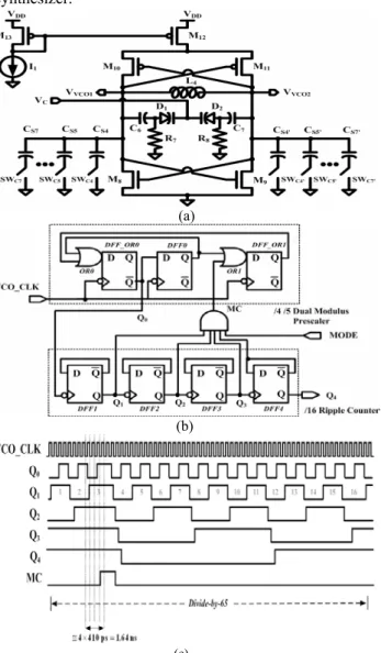
B. Frequency Synthesizer with Tunable VCO
Most modern frequency synthesizers with on-chip VCO utilize a phase locked loop technique to control the output frequency precisely with reference to a fixed frequency. The frequency synthesizer consists of a LC-tank VCO, a crystal oscillator, a programmable frequency divider, a phase-frequency detector (PFD), a charge pump (CP), and a loop filter. To fully integrate the phase-locked loop (PLL) frequency synthesizer, phase noise and spurious suppression must be traded off against integrated capacitance and settling time. The LC-tank VCO is the most key component in the frequency synthesizer.
(a)
(b)
(c)
Fig. 4. (a) Tunable LC-tank VCO circuit. (b) Logic block diagram of the prescaler (c) Timing diagram of the prescaler.
Figure 4(a) shows the circuit diagram of a tunable LC-tank VCO. The architecture of VCO in this design is a complementary LC oscillator. NMOS and PMOS are connected as cross-coupled to generate negative resistance. L4 is the on-chip spiral inductor with 3.7nH
inductance. The varactor is implemented by P+/N-well junction capacitor. In order to reduce sensitivity to power supply, the DC blocking capacitors are series connected to the varactor with grounded resistor. The other advantage of this topology is the controlled voltage can be full swing between supply voltage and ground. M8 and M9
(M10 and M11) are cross-connected as positive feedback to
form the negative resistor. M11 acts a tunable current source to control the output swing of the VCO. By means of selective switches (SWCi), linear capacitors (CSi, i = 4, 5~7) are utilized to universal tune the frequency band of the VCO to improve the yield rate in the mass production. The auto-tuning mechanism will be implemented in the future to reduce the test cost.
Figures 4(b) and 4(c) show a logic block and associated timing diagram of the prescaler. The use of variable modulus prescaler at high frequency instead of using a fixed frequency prescaler has an advantage that only the prescaler works at high frequency while the remaining divider circuitry works at much lower frequencies. This saves the power, reduces the cost, and makes the layout of the divider relatively noncritical. The main contributors to the PLL synthesizer power consumption are VCO (up to 70%, 23 mW) and frequency divider (up to 30%, 9 mW). The phase noise contribution of the prescaler to the phase of frequency synthesizer is usually negligible. The overall noise from the prescaler is much lower than that of crystal reference multiplied by the prescaler ratio.
C. IF Section
A new low-power 10.7-MHz IF section including a limiting amplifier and FM/FSK demodulator is proposed. A limiting amplifier is usually selected as a magnitude limitation in FM/FSK applications rather than automatic gain control since the circuitry is simple. However, dc offset may be so large that it reduces the sensitivity and therefore degrades the recovered data bit-error rate (BER).
Fig. 5. Block diagram of the limiting amplifier with gain cell.
The limiting amplifier is implemented by cascaded of seven identical gain cells comes with an auxiliary output driver. To extract dc offset voltage, a large discrete capacitor is necessary to save chip area. The limiting amplifier is basically an amplifier chain that enlarges different magnitudes of input signal into saturation.The FM/FSK demodulator employs a quadrature detector that is composed of an on-chip phase detector and an external tank phase shifter to achieve high discrimination function under low-voltage operation. The proposed quadrature detector, based on the multiplier output proportional to two input variables, for FM/FSK demodulation is shown in Fig. 5(c). The frequency to voltage conversion gain of the demodulator is 15 mV/kHz and the dynamic range of the limiting amplifier is 80dB. The sensitivity of the IF section including demodulator and limiting amplifier is –72 dBm. The power consumption of the proposed IF section is 14 mW.
4.
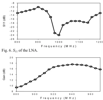
Summarized Measured ResultsDue to the input impedance of the LNA is designed to around 50Ω over the large frequency bandwidth, the S11
of the receiver input is smaller than –9 dB. Fig. 6 shows the S11 versus the frequency. The minimum value of the
S11 is occurred at 1-GHz. So, the receiver can get the
maximum power transfer from the antenna. In order to get the maximum performance, no buffers are used after LNA for measurement. The conversion gain of the RF front-end including LNA and mixer is measured with 10.7-MHz IF frequency. F r e q u e n c y ( M H z ) 8 0 0 9 0 0 1 0 0 0 1 1 0 0 1 2 0 0 S11 (dB) - 2 6 - 2 4 - 2 2 - 2 0 - 1 8 - 1 6 - 1 4 - 1 2 - 1 0 - 8
Fig. 6. S11 of the LNA.
F r e q u e n c y ( M H z ) 8 8 0 9 0 0 9 2 0 9 4 0 9 6 0 Ga in (dB ) 8 1 0 1 2 1 4 1 6 1 8 2 0
Fig. 7. Conversion gain of the ISM receiver’s front-end. The frequency response of the RF front-end is shown in Fig. 7. The conversion gain is large than 11 dB over the ISM band. Figure 8 shows the noise figure of the RF front-end, which is less than 9 dB. The minimum noise figure of 5 dB is obtained at the RF front-end with a maximum conversion gain. The IIP3 of the RF front-end is measured by two applied tones with spacing of 1 MHz.
F r e q u e n c y ( M H z ) 8 8 0 9 0 0 9 2 0 9 4 0 9 6 0 Noi se Figure (dB) 4 6 8 1 0 1 2 1 4
Fig. 8. Noise figure of the ISM receiver’s front-end.
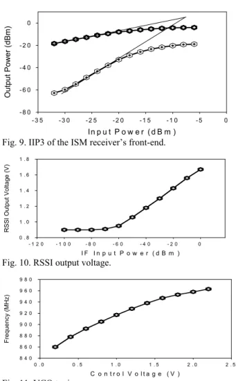
In p u t P o w e r ( d B m ) - 3 5 - 3 0 - 2 5 - 2 0 - 1 5 - 1 0 - 5 0 Ou tput P owe r ( dBm ) - 8 0 - 6 0 - 4 0 - 2 0 0
Fig. 9. IIP3 of the ISM receiver’s front-end.
I F I n p u t P o w e r ( d B m ) - 1 2 0 - 1 0 0 - 8 0 - 6 0 - 4 0 - 2 0 0 RSS I Out put Vol tag e ( V ) 0 . 8 1 . 0 1 . 2 1 . 4 1 . 6 1 . 8
Fig. 10. RSSI output voltage.
C o n t r o l V o l t a g e ( V ) 0 . 0 0 . 5 1 . 0 1 . 5 2 . 0 2 . 5 F requenc y (MHz) 8 4 0 8 6 0 8 8 0 9 0 0 9 2 0 9 4 0 9 6 0 9 8 0
Fig. 11. VCO tuning range.
The IIP3 of the RF front-end is –8 dBm as shown in Fig. 9. This specification is appropriate for many applications such as wireless mouse, wireless keyboard, etc. With 0.1% BER, the sensitivity at IF input of the receiver is –72 dBm. The maximum signal power of the demodulator can demodulate at IF input is 8 dBm. In an IF section, the limiting amplifier has a RSSI function. The RSSI output voltage versus the IF input power is shown in Fig. 10. When the IF input power is larger than –60 dBm, the curve is quite linear as shown in Fig. 10. In the limiter design, the current consumption is only 3 mA. The measured voltage gain is 78 dB over a 12 MHz bandwidth. In the proposed receiver, the quadrature demodulator is used to demodulate the FSK receiver signal. The current consumption is only 1 mA in the demodulator. The receiver data rate with 390 kbps can be achieved and the receiver sensitivity is –80 dBm with 0.1% BER.
In Fig. 11, the tuning characteristic measured from the on-chip LC VCO shows a tuning frequency range of 110 MHz varying from 860 to 970 MHz as the controlled voltage is changed between 0.2 V and 2.3 V. As the oscillation frequency of the quadrature VCO varies between minimum and maximum in terms of the tuned range, the simulated peak-to-peak voltage swing of the quadrature VCO is around 1 VP-P. Therefore, the
oscillation of the quadrature VCO occurs in the regime of limited current. This large swing signal can make the switching MOS in Gilbert mixer function properly and reduces the noise from the switching MOS. A microphotograph of the ISM receiver chip is shown in Fig. 12. Measured performances of the ISM receiver IC are summarized in Table 1.
Fig. 12. Chip photo.
Table 1. Summary of Tunable ISM Receiver Power Supply Voltage 2.7~3.6 V Current Consumption 33 mA S11 -13 dB RF Gain 15 dB IIP3 -8 dBm Noise Figure 5 dB Dynamic Range 80 dB
VCO Tuning Range 860~963 MHz
LO Leakage -50 dBm
Data Rate 390 kbps
Sensitivity@0.1%BER -80 dBm
Technology 0.25-um SP5M CMOS
REFERENCES
[1] J. Crols and M. Steyaert, “A single-chip 900 MHz receiver front-end with a high performance low-IF topology,” IEEE J. Solid-State Circuits, vol. 30, pp. 1483-1492, 1995.
[2] D.K. Shaeffer, et al, “A 115-mW, 0.5µm CMOS GPS Receiver with Wide Dynamic-Range Active Filters,”
IEEE J. Solid-State Circuits, vol. 33, pp.
2219-2231,1998.
[3] P. Orsatti, F. Piaaza, Q. Huang, “A 20-mA-Receiver, 55-mA-Transmit, Single-Chip GSM Transceiver in 0.25µm CMOS,” IEEE J. Solid-State Circuits, vol. 34, pp. 1869-1880, 1999.
[4] M. Driscoll and T. Merrell, “Spectral Performances of Frequency Multiplier and Dividers,” Proc. 46th Annual
Frequency Control Symp., pp.193-200, 1992.