國 立 交 通 大 學
電機資訊學院電子與光電學程
碩 士 論 文
深次微米低壓次能帶隙電壓參考源電路
設計
Low Voltage Sub-Bangdap Voltage Reference Circuit
Design in Deep Sub-Micron Process
研 究 生 : 謝 禎 輝
指導教授 : 吳 錦 川 教授
中華民國 九十四 年 九 月
深次微米低壓次能帶隙電壓參考源電路
設計
Low Voltage Sub-Bangdap Voltage Reference Circuit
Design in Deep Sub-Micron Process
研 究 生: 謝 禎 輝 Student : Chen-Hui, Hsieh
指導教授: 吳 錦 川 Advisor : Jiig-Chuan Wu
國 立 交 通 大 學
電機資訊學院電子與光電學程
碩 士 論 文
A Thesis
Submitted to Degree Program of Electrical Engineering Computer
Science
College of Electrical Engineering and Computer Science
National Chiao Tung University
in Partial Fulfillment of the Requirements
for the Degree of
Master of Science
in
Electronics and Electro-Optical Engineering
June 2005
Hsinchu, Taiwan, Republic of China
授權書
(博碩士論文) 本授權書所授權之論文為本人在_____國立交通____大學(學院)___電子___系所 __電子與光電_組_九十四_學年度第_一_學期取得_碩_士學位之論文。 論文名稱:深次微米低壓次能帶隙電壓參考源電路設計 1.■同意 □不同意 本人具有著作財產權之論文全文資料,授予行政院國家科學委員會科學技術資料中心、國家圖書館及本 人畢業學校圖書館,得不限地域、時間與次數以微縮、光碟或數位化等各種方式重製後散布發行或上載 網路。 本論文為本人向經濟部智慧財產局申請專利的附件之一,請將全文資料延後兩年後再公開。(請註明文 號: ) 2.■同意 □不同意 本人具有著作財產權之論文全文資料,授予教育部指定送繳之圖書館及本人畢業學校圖書館,為學術研 究之目的以各種方法重製,或為上述目的再授權他人以各種方法重製,不限地域與時間,惟每人以一份 為限。 上述授權內容均無須訂立讓與及授權契約書。依本授權之發行權為非專屬性發行權利。依本授權所為之收錄、重 製、發行及學術研發利用均為無償。上述同意與不同意之欄位若未鉤選,本人同意視同授權。 指導教授姓名:吳錦川
研究生簽名: 學號:9067515 (親筆正楷) (務必填寫) 日期:民國 94 年 9 月 日 1. 本授權書請以黑筆撰寫並影印裝訂於書名頁之次頁。 2. 授權第一項者,所繳的論文本將由註冊組彙總寄交國科會科學技術資料中心。 3. 本授權書已於民國 85 年 4 月 10 日送請內政部著作權委員會(現為經濟部智慧財產局)修正定稿。 4. 本案依據教育部國家圖書館 85.4.19 台(85)圖編字第 712 號函辦理。國 立 交 通 大 學
論 文 口 試 委 員 會 審 定 書
本校 電機資訊學院專班
電子與光電
組
謝禎輝 君
所提論文
(中文)
深次微米低壓次能帶隙電壓參考源電路設計
(英文)
Low Voltage Sub-Bangdap Voltage Reference CircuitDesign in Deep Sub-Micron Process
合於碩士資格水準、業經本委員會評審認可。
口試委員: 吳錦川 黃振昇
柯明道 邱進峰
指導教授: 吳錦川 博士
班主任: 郭仁財 博士
中 華 民 國 94 年 9 月
學生:謝禎輝
指導教授:吳錦川 教授
國立交通大學電機資訊學院 電子與光電學程﹙研究所﹚碩士班
摘
要
此論文提出一個能操作在 1-V 電源電壓下之次能帶隙電壓參考源. 且其 參考電壓輸出亦為低於 1-V 之電路架構. 所完成的晶片是一個適用於電池供 電的系統整合晶片之應用。目的是能夠實現一個簡單,穩定,低成本,低電 壓,低功率消耗的參考電壓源而能夠很容易的使用在可攜式裝備上。 這個晶片的製作是以台灣積體電路製造股份有限公司提供的 90nm 低功 率互補式金氧半導體製程技術實現。整個晶片設計包含一個低壓運算放大 器,電流鏡,及一個次能帶隙電壓產生器核心電路。 量測結果顯示,次能帶隙電壓參考源可以操作在 1-V 電源電壓。 但其 輸出參考電壓會隨電壓源而變動。為改善此特性,重新設計了低壓運算放大 器,電流鏡,低電壓啟動器,及加入一個直流偏壓源。模擬結果顯示輸出參考 電壓不再會隨電壓源而變動,且其工作電壓能低至 0.8 伏特並具有溫度係數 60ppm/°C。在 1-V 電源電壓下有 44µW 的功率消耗。
Sub-Micron Process
Student:Chen-Hui Hsieh
Advisor:Prof. Jiig-Chuan Wu
Degree Program of Electrical Engineering Computer Science
National Chiao Tung University
ABSTRACT
This thesis proposed a design of 1-V sub-bandgap voltage reference generator circuit. It is suitable for battery-based System-On-Chip applications. The goal of this design is to realize a simple, low cost, low voltage, and low power consumption sub-bandgap voltage reference generator and it can be easy to use for portable equipments.
This chip was fabricated using TSMC 90nm CMOS logic process technology provided by Taiwan semiconductor manufacturing company. Whole chip includes a low voltage operational amplifier, current source, and a sub-bandgap core voltage generator circuit.
The measured results show that the sub-bandgap voltage reference generator can be operated at 1-V power supply, but the output reference voltage will vary with power supply. To improve the circuit performance, the low voltage operational amplifier, the current mirror and low voltage start up circuit are re-designed, in additional with a DC bias circuit. The simulation result shows the VDDmin can achieve 0.8V with 60ppm/°C in new circuit. The power dissipation is 44µW with 1-V power supply.
First, I express my deepest gratitude to my advisor, Professor Jiig-Chuan Wu for his enthusiastic, patient direction and invaluable suggestions.
I thank to top managements of Design Service Division in TSMC, Dr. Ping Yang, Dr. Fred Wang, Dr. Mark Chen and Dr. Mi-Chang, who supported me to pursue t- he master degree of science engineering in NCTU.
I also thank to my colleagues Andy Yang, Dar Sun and Lawrence Wu. They always enthusiastically give me suggestions and help in circuit layout, test chip measurements and thesis document preparation.
I thank my parents, who encouraged me to do what I like to do, and supported me in all achievements. In addition, I give my dearly thank to my wife, Grace Chen. She was always the driving force to push me to move forward, and I share all my honors with her.
Finally, I would like to say thank to all the people who have ever helped me in the past years.
Contents
Chinese Abstract
………
i
English Abstract ……… ii
Acknowledgments ……… iii
Contents ………
iv
Figure Captions
……… vi
Table Captions ………
vii
CHAPTER 1 Introduction ...1
1.1 Background ...1
1.2 Review Bandgap Reference Architecture...3
1.3 Motivation ...9
1.4 Thesis organization ...10
CHAPTER 2 Circuit Architecture And Measurement Result ...11
2.1 System Architecture ...11
2.2 Operational Principle...12
2.3 Circuit Design And Simulation Result...14
2.4 Sub-Bandgap Circuit Realization...19
2.5 Measurement Result...21
2.6 Explanation Of Simulation And Measurement’s Discrepancy ...22
3.2 Low Voltage OPAMP’s Enhancement...30
3.3 Start Up Circuit For Low Voltage Operation ...33
3.4 Simulation Results Of Enhanced Circuit ...36
3.5 The New Scheme To Enhance VDDmin Performance ...36
CHAPTER 4 Conclusion And Future Works...41
4.1 Conclusions ...41
CHAPTER 1 INTRODUCTION...1
Fig 1.1 The trend of system integration. ...1
Fig. 1.2 The trend of operation voltage in CMOS technology...2
Fig. 1.3 Bandgap voltage reference architecture...4
Fig. 1.4 Simple implementation of bandgap voltage reference...4
Fig. 1.5 Resistive divided sub-bandgap architecture ...6
Fig. 1.6 NMOS input stage of OPAMP’s architecture...8
Fig. 1.7 PMOS input stage of OPAMP’s architecture ...9
CHAPTER 2 CIRCUIT ARCHITECTURE AND MEASUREMENT RESULTS ...11
Fig. 2.1 1-V sub-bandgap block diagram...11
Fig 2.2 The operation of sub-bandgap circuit ...13
Fig 2.3 1-V Sub-bandgap circuit...16
Fig 2.4 Current Mirror in the amplifier...17
Fig 2.5 Simulation result...18
Fig 2.6 The GDS file of 1-V Sub-bandgap circuit ...20
Fig 2.7 1V Sub-bandgap circuit’s silicon...21
Fig 2.10 The BJT’s simulation log file ...23
Fig 2.11 Resistance vs. Temp. of V1.0 Resistor model ...25
Fig 2.12 Resistance vs. Temp of V1.3 resistor model ...25
Fig 2.13 The Ids of p23 versus Temp by model V1.0 and V1.3. ...26
Fig 2.14 The bandgap voltage output using V1.3 model ...26
Fig 2.15 The good correlation between simulation and measurement data...27
CHAPTER 3 CIRCUIT ENHANCEMENT AND SIMULATION RESULTS ...28
Fig 3.1 The bias circuit correction of 1-V sub-bandgap circuit ...29
Fig 3.2 The enhanced low voltage OPAMP...31
Fig 3.3 The LV amplifier ...32
Fig 3.4 The operation point of current source...34
Fig 3.5 The 1V Sub-bandgap circuit...34
Fig 3.6 The 1-V sub-bandgap circuit with start up circuit ...35
Fig 3.7 Enhanced circuit BJT’s simulation log...37
Fig. 3.8 The Vref of enhanced Sub-bandgap circuit ...38
Fig 3.9 The sub-bandgap circit with DC bias circuit ...39
CHAPTER 4 CONCLUSIONS AND FUTURE WORKS...41
Table Captions
CHAPTER 1
INTRODUCTION
1.1 BACKGROUND
Voltage reference is always a pivotal building block in mixed-signal integrated system and high- density memory, like DRAM and Flash memory devices. Recently there has been a growing demand on low battery supply applications such as cell phones and highly integrated System-On-Chip devices has created needs to design systems capable of operating from a single 1-V power supply as well as voltage reference. For example, a generic System-On-Chip device, as shown in Fig. 1.1, has more than one voltage reference due to different voltage reference requirements in system design. In such a system, one voltage reference is needed for I/O interface circuit to convert external signal’s voltage level to internal’s signal voltage level, and another voltage reference is needed for power management unit, which includes many on-chip DC to DC power converters to provide regulated power for multiple sub-blocks in system. Some other voltage references are needed for ADCs and DACs, which need high accuracy reference voltage to provide high-resolution data conversions.
Power Management Unit
ARM, DSP, micro-system I/ O In te rf ac e I/ O Int erf ac e DAC ADC PLL & clock REF REF REF REF SOC
Power Management Unit
ARM, DSP, micro-system I/ O In te rf ac e I/ O Int erf ac e DAC ADC PLL & clock REF REF REF REF SOC Fig 1.1 The trend of system integration.
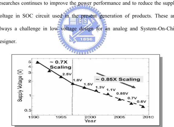
In additional to the application’s multiple reference voltage generators demands, the deep sub-micron CMOS process technology needs supply voltage scaling down with process technology scaling. Two primary reasons for scaling the supply voltage are to maintain the power density of an integrated circuit below a limit, which can be supported by cost effective cooling techniques, and to guarantee the long-term reliability of manufactured devices. Please refer to Fig 1.2, which indicates the supply voltage could be lower than 1.0 V when process technology enter 90nm era. The low voltage circuit design becomes mainstream due to hand-held applications and process technology required. A great amount of researches continues to improve the power performance and to reduce the supply voltage in SOC circuit used in the present generation of products. These are always a challenge in low voltage design for an analog and System-On-Chip designer.
Fig. 1.2 The trend of operation voltage in CMOS technology.
A conventional bandgap reference circuit does not permit an output voltage below 1.2 V, which is nearly the same voltage as the bandgap of silicon. Therefore, the conventional bandgap reference circuit is neither suitable for low voltage
System-On-Chip device ‘s application, nor for low reference voltage output, which may need in 1-V integrated circuit system. To achieve sub-bandgap reference voltage output, the special circuit techniques are required.
The specification of this sub-bandgap voltage reference design is based on low supply voltage 1.2V – 1.0V System-On-Chip requirement and sub-bandgap output reference voltage need to be programmable to be adapted by system flexibly. The temperature coefficient should be below 100ppm/°C, which is a generic specification in most applications.
In this thesis, the sub-bandgap voltage reference was fabricated using a 90nm standard CMOS process provided by TSMC. This design uses operating voltage from 1.2V to 0.8V and measured in 0°C to 100°C temperature environment. The main architecture of this low voltage sub-bandgap voltage reference generator is composed by resistive divided sub-bandgap core plus low voltage operational amplifier.
1.2 REVIEW BANDGAP REFERENCE ARCHITECTURES
The working principle of a bandgap voltage reference generator is illustrated in Fig. 1.3. A voltage VBE is generated from a pn-junction diode having a
temperature coefficient of approximately –2.2 mv/°C at room temperature. Also generated is a thermal voltage VT (= kT/q), which is proportional to absolute
temperature (PTAT) and has a temperature coefficient of +0.085 mv/°C at room temperature. If the VT voltage is multiplied by a constant K and summed with the
VBE voltage, then the output voltage is given as
BE T
V
V
+
=K
Since the VBE has little dependence on the power supply, the power supply
dependence of the bandgap reference will be quite small.
q kT = T V
å
VREF= KVT+ T V K T V K BE VFig. 1.3 Bandgap voltage reference architecture
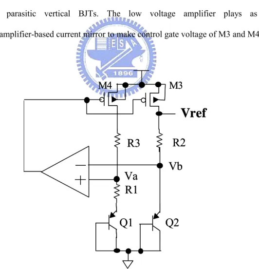
BE
V
The above-mentioned concept can be implemented as shown in Fig 1.4 by using parasitic vertical BJTs. The low voltage amplifier plays as a error-amplifier-based current mirror to make control gate voltage of M3 and M4.
Vref
Q1
Q2
R1
R2
M4
M3
R3
Va
Vb
Vref
Q1
Q2
R1
R2
M4
M3
R3
Va
Vb
Ideally, the amplifier has a high voltage gain A, and therefore, Va = Vb can be
achieved. When R2 = R3, and VDS1 = VDS2 can be easily obtained to provide a
good current match by M3 and M4. The Vref output voltage of this bandgap structure is as below. 25 . 1 ln V Vref 2 1 T 1 2 EB2 ≈ úû ù êë é + = A A V R R (2)
The VDDmin of bandgap is limited by Vsd(sat) of M3 device plus the Vref output voltage. Generally, the VDDmin limited by equation (3) is 1.2V + 0.3V = 1.5V.
{
V
}
V
V
3min
DD
=
ref+
SDsat (3)But there have another VDDmin limitation is caused by amplifier’s ICMR, which is input common mode voltage range. The VDDmin of amplifier limited by ICMR is as follow:
{
V
}
V
2V
2
V
SDsatmin
DD
=
EB + TP + (4)The VDDmin limited by amplifier’s ICMR is 0.7V + 0.4V +2X (0.3V) = 1.7V, assuming Vtp = - 0.4Vand Vsd(sat) = 0.3V. Therefore, conventional bandgap’s VDDmin is limited by amplifier’s ICMR. To achieve a low voltage bandgap voltage reference, then we need to overcome the ICMR issue in low voltage amplifier.
We finish review conventional bandgap circuit’s limitations, now we start to review the most up-to-dated sub-bandgap voltage reference generator and low voltage (< 1-V) bandgap voltage reference generator.
A. Resistive divided sub-bandgap
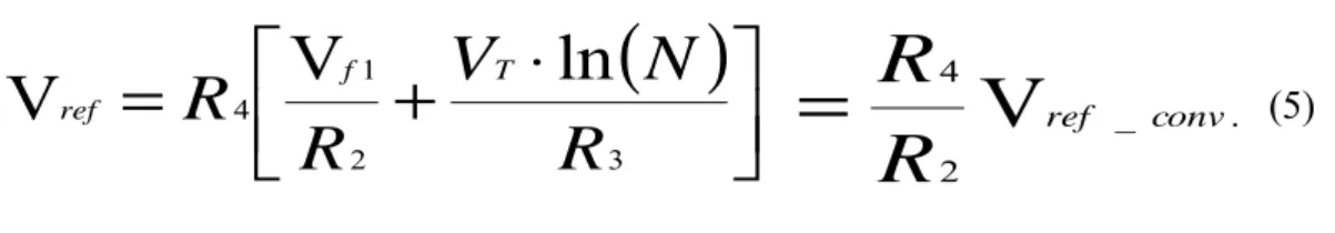
This is probably the most commonly employed architecture in current sub-bandgap voltage reference circuit. The concept is basically a current mode method to scale down the bandgap reference voltage by a factor defined by a resistor ratio. Vref R1 R2 M1 R4 R3 M2 M3 Vb Va Vb OPA I D1 ID2 ID3 Vf1 Va Vref R1 R2 M1 R4 R3 M2 M3 Vb Va Vb OPA I D1 ID2 ID3 Vf1 Va
Fig. 1.5 Resistive divided sub-bandgap architecture
Fig 1.5 shows the circuit proposed by Banba. The reference voltage is form by two currents I1 and I2. For I1, it is a PTAT current formed by D1, D2 and R2 as given by V1=VTln(N)/R1, while I2 is a current due to VD2 and R2 as given by I2=VD2/R2, thus Vref is given by below equation (5).
( )
úû
ù
êë
é
+
⋅
=
3 2 1 4ln
V
V
R
N
V
R
R
f T ref _ . 2 4V
ref convR
R
=
(5)The temperature dependence of the reference voltage can be cancelled by and appropriate R2/R1 ratio and N. A resistor ratio of R4/R2, which is less than one, is used to scale down the bandgap voltage reference to be less than 1.2V. Therefore, the magnitude of Vref can be adjusted for different applications.
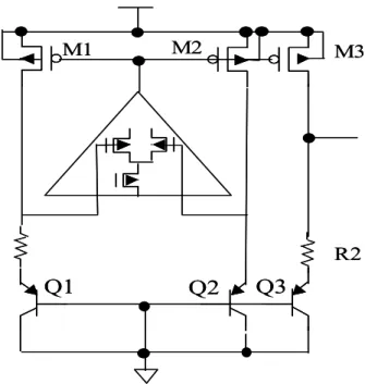
B. Low Voltage bandgap voltage reference generator
In CMOS technology, a parasitic vertical BJT formed in a P- or n-well is commonly used to implement a bandgap reference. The minimum supply voltage needs to be greater than 1V due to two factors. The first factor is the reference voltage is around 1.25V, which exceeds 1-V supply voltage. We can overcome this problem by using above-mentioned concept, which use resistive subdivision method to scale down the 1.25V reference voltage. The second factor is low voltage design of PTAT current generation loop is limited by the common collector structure of the parasitic vertical BJT’s Vbe voltage or the input common-mode voltage of the operational amplifier. The second problem can be solved by BiCMOS or by using low threshold voltage devices. In this thesis, we will provide one new scheme to overcome the second factor discuss above.
As shown in Fig 1.6, the minimum input commo-mode voltage of an amplifier with an NMOS input stage must be less than VEB(on), which implies that
Vthn< 0.6V is required (assumed VEB(on) = 0.7V and VDS(sat) = 50mv). This is acceptable as NMOS device with Vthn < 0.6V can be easily found in many CMOS process technology.
However, the temperature effect on the base-emitter voltage and the threshold voltage of NMOS device need to be considered. The temperature coefficient of the base-emitter voltage is approximately –2.2 mv/°C while the threshold voltage of NMOS may be greater than –2.2 mv/°C. At high temperature, VEB(on) may be less than Vthn + 2VDS(sat), and the reference circuit will not function properly. Thus, either native NMOS device or NMOS transistor with Vthn < 0.5V are required to allow the reference circuit in Fig 1.6 to operate down to a single 1-V supply.
Q1 Q2 R2 M2 M3 Q3 M1 Q1 Q2 R2 M2 M3 Q3 M1
Fig. 1.6 NMOS input stage of OPAMP’s architecture
{
ICMR}
Vthn 2VDSsat VEB(on)min = + < (6)
In Fig 1.7 shown the PMOS input stage of bandgap reference generator. The minimum supply voltage of this structure is VEB(on) + Vthp + 2VDS(sat), and therefore Vthp less than 0.2V is required to implement a 1-V reference.
Fig. 1.7 PMOS input stage of OPAMP’s architecture
Vref
Q1
Q2
R1
R2
M3
M2
M1
Q3
1.3 MOTIVATION
TSMC 90m 1P9M 1.0V generic process technology is a mature and stable process technology for today’s high-end System-On-Chip applications. Its standard supply voltage is 1.0V. Most of portable system consuming low power has become a new trend in circuit design. This thesis tries to realize a 1-V low voltage sub-bandgap circuit fabricated by TSMC 90nm process for low voltage and low power application. By using standard MOS devices in TSMC 90nm technology, we don’t need additional circuit techniques to realize low voltage sub-bandgap circuit architecture. The VDDmin can be achieved below 1.0V, but the temperature coefficient become worse (>100 ppm/°C) when VDD is less than 1.0V. In this thesis, we propose one new scheme to bring VDDmin down to 0.8V without scarifying temperature coefficient. Low voltage design in analog circuit is challenging in deep sub-micron process technology.
1.4 THESIS ORGANIZATION
In this chapter, the thesis discussed about the principle of different bandgap architecture and their advantages and disadvantages. In the next chapter, chapter 2, it presents the design of low voltage sub-bandgap circuit in detail and their design considerations. Silicon measurement versus simulation is presented, and bandgap’s silicon characteristics is not as expected. The discrepancy between simulation and measurement was debugged. A correction simulation was done to correlate the measurement data with simulation. Therefore, in Chap 3 we present the circuit performance enhancement and simulation results. Each sub-block is simulated and discussed separately. The simulation result shows 1-V sub-bandgap circuit hardly meets the design targets, but with one additional DC bias voltage source the design meets the targets. Finally, conclusions and future works are described in chapter 4.
CHAPTER 2
CIRCUIT ARCHITECTURE AND
MEASUREMENT RESULTS
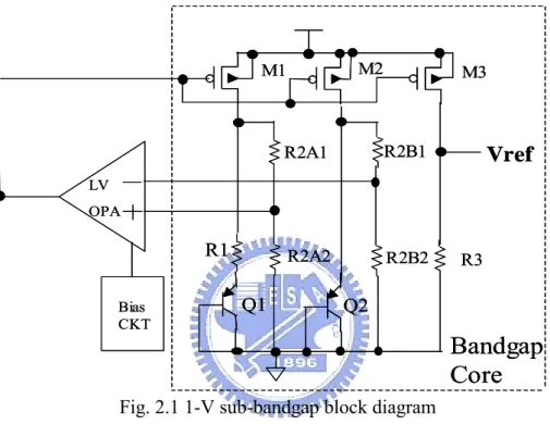
2.1 SYSTEM ARCHITECTURE
Vref
Q1 Q2 R1 R2A2 M1 R3 Bias CKT LV OPA R2A1 R2B1 R2B2 M2 M3Bandgap
Core
Vref
Q1 Q2 R1 R2A2 M1 R3 Bias CKT LV OPA R2A1 R2B1 R2B2 M2 M3Bandgap
Core
Fig. 2.1 1-V sub-bandgap block diagram
The block diagram of 1-V sub-bandgap architecture is shown in Fig. 2.1. The 1-V sub-bandgap architecture includes a low voltage amplifier, bias circuit, and bandgap core circuit.
The low voltage amplifier provides a medium gain to form the PTAT current loop. The bias circuit just provides stable bias voltage to low voltage amplifier. The bandgap core is a resistive division bandgap core, which mention in chapter 1.
Layout and design strategies are considered to achieve high performance and low voltage operation in this architecture. The whole chip floorplan, the symmetry
of differential circuit, robust power line, and device matching are the key points to eliminate the ill effects in layout.
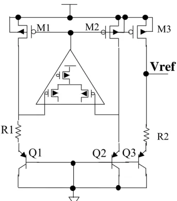
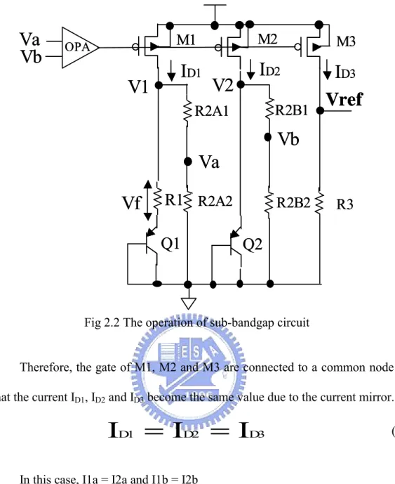
2.2 OPERATIONAL PRINCIPLE
This section describes the operation principle of the sub-bandgap circuit, and it presents how the sub-bandgap reference voltage is generated.
The concept of the sub-bandgap reference is that two currents, which are proportional to Vf and VT, are generated by only one feedback loop. Fig 2.2 presents the block diagram of sub-bandgap circuit. The PMOS transistor dimensions of M1, M2 and M3 are the same, and the resistance of R2A = R2A1 + R2A2 is the same as R2B = R2B1 + B2B2.
B
R
A
R
2
=
2
(7)The low voltage amplifier is so controlled that the voltage of Va and Vb are equalized under all conditions.
b
a
V
Vref
Q1
Q2
R1
R2A2
M1
R3
R2A1
R2B1
R2B2
M2
M3
Va
Vb
Va
Vb
V1
V2
OPAI
D1I
D2I
D3Vf
Vref
Q1
Q2
R1
R2A2
M1
R3
R2A1
R2B1
R2B2
M2
M3
Va
Vb
Va
Vb
V1
V2
OPAI
D1I
D2I
D3Vf
Fig 2.2 The operation of sub-bandgap circuit
Therefore, the gate of M1, M2 and M3 are connected to a common node so that the current ID1, ID2 and ID3 become the same value due to the current mirror.
D3 D2
D1
I
I
I
=
=
(9)In this case, I1a = I2a and I1b = I2b
(
N
ln
V
V 2
-V
V 1
-V
V
f=
BE1=
BE1=
Td
)
(10) I2a is proportional to VT.1
R
dV
I
2a=
f (11) I2b is proportional to Vf1.2
R
V
I
2b=
Ε Β 2 (12)I2 is the sum of I2a and I2b, and I2 is mirrored to I3.
b
2
a
2
2
D
3
D
I
I
I
I
=
=
+
(13)Therefore, the output voltage of the sub-bandgap Vref becomes as follow:
úû
ù
êë
é
⋅
÷
ø
ö
ç
è
æ
+
⋅
=
⋅
=
D3 EB2ln
N
V
TR1
R2
V
R2
R3
R3
I
Vref
(14)If the resistor and BJT parameters for this sub-bandgap are the same as those for the conventional bandgap, then Vref is simplified as
ref_conv ref
V
2
3
V
R
R
=
(15)Therefore, Vref can be freely changed from Vref_conv. The Vref is determined by the resistance ratio of R1, R2, and R3 and little influenced by the absolute value of the resistance. The transistor M1, M2, and M3 are required to operate in the saturation region, so that their VDS voltage can be small when IDS currents are reduced.
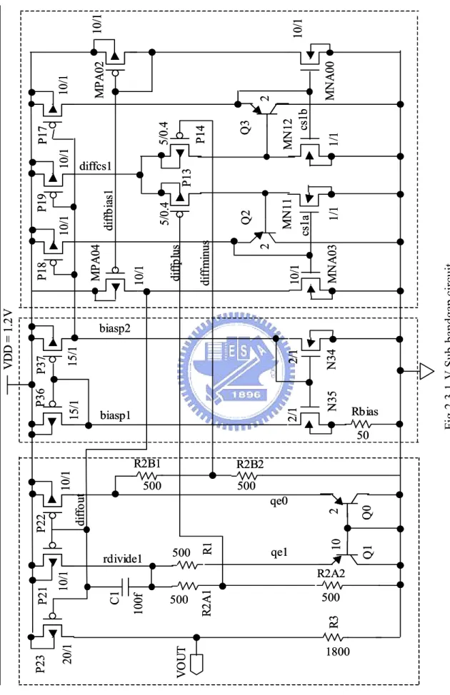
2.3 CIRCUIT DESIGN AND SIMULATION RESULT
Fig 2.3 shows the schematic diagram of sub-bandgap design. Whole sub-bandgap circuit is made of three portions: 1. bandgap core circuit; 2. low voltage amplifier; 3. biasing circuit. The bandgap core circuit is designed according to section 2.2 described. The low voltage amplifier needs a DC
level-shifting current mirror in order to make the low voltage amplifier function properly, especially for some technologies with Vthn > vthp. The circuit shown in Fig 2.5 is part of the amplifier in Fig 2.3 without dc level-shifting current mirror. The Vds of P13 is given by Vin+ + Vgs13 – Vgs11 ~ Vin+, assuming Vgs13 ~ Vgs11 for Vthp ~ Vthn. If Vthn > Vthp, the Vds of P13 is less than Vin+. The Vds of P13 may be less than the saturation voltage if Vin+ is small and P13 may operate in the triode region and this reduce the gain of amplifier.
A DC level-shifting current mirror using the parasitic vertical BJT can solve this problem. The drain-source voltage of P13 is now given by Vin+ + Vgs13 + VEB2 – Vgs10. This ensure that P13 will operate in the saturation region even when Vin+ = 0V, based on the Vthn is not greater than vthp by more than 0.6V. The bias circuit generates bias voltage for MP19 of amplifier.
Fig 2.3 1-V Sub-bandgap circuit R3 P36 P3 7 P1 8 P1 9 P1 7 VO U T 10 /1 10 /1 20 /1 10 /1 Q1 Q0 1800 R2A2 500 500 500 R2 A 1 R1 10 2 2/ 1 50 500 500 P23 P21 P22 15/ 1 15 /1 10 /1 10/ 1 10 /1 10 /1 5/ 0. 4 5/ 0.4 10 /1 MP A 04 MP A 02 P1 3 P1 4 MN 11 MN 12 1/ 1 1/ 1 Q2 Q3 22 MN A 00 MN A 03 10 /1 2/ 1 C1 10 0f R2B1 R2B2 Rbias N3 5 N3 4 di ffo ut qe0 qe1 rdivide1 di ff p lus di ff m in us di ffb ia s1 VD D = 1 .2 V diffcs1 cs1 b cs 1a biasp2 biasp1 R3 P36 P3 7 P1 8 P1 9 P1 7 VO U T 10 /1 10 /1 20 /1 10 /1 Q1 Q0 1800 R2A2 500 500 500 R2 A 1 R1 10 2 2/ 1 50 500 500 P23 P21 P22 15/ 1 15 /1 10 /1 10/ 1 10 /1 10 /1 5/ 0. 4 5/ 0.4 10 /1 MP A 04 MP A 02 P1 3 P1 4 MN 11 MN 12 1/ 1 1/ 1 Q2 Q3 22 MN A 00 MN A 03 10 /1 2/ 1 C1 10 0f R2B1 R2B2 Rbias N3 5 N3 4 di ffo ut qe0 qe1 rdivide1 di ff p lus di ff m in us di ffb ia s1 VD D = 1 .2 V diffcs1 cs1 b cs 1a biasp2 biasp1
P18 P1 9 10/ 1 10/ 1 5/ 0.4 MP A 0 4 P1 3 MN 1 1 1/ 1 Q2 2 MN A 0 3 10/ 1 d iffp lu s VD D = 1 .2 V diffcs1 cs1 a P1 9 10/ 1 5/ 0 .4 P1 3 MN 1 1 1/ 1 MN A 0 3 10 /1 d iffp lu s VDD = 1 .2 V diffcs1 cs 1a Vg s1 1 Vd s1 3 Vd s1 3 Vg s1 1 Vg s1 3 Vg s1 3
W
it
h
out
D
C
le
v
el s
h
if
ti
n
g
Wi
th
D
C
le
v
el
s
h
if
ti
n
g
P18 P1 9 10/ 1 10/ 1 5/ 0.4 MP A 0 4 P1 3 MN 1 1 1/ 1 Q2 2 MN A 0 3 10/ 1 d iffp lu s VD D = 1 .2 V diffcs1 cs1 a P1 9 10/ 1 5/ 0 .4 P1 3 MN 1 1 1/ 1 MN A 0 3 10 /1 d iffp lu s VDD = 1 .2 V diffcs1 cs 1a Vg s1 1 Vd s1 3 Vd s1 3 Vg s1 1 Vg s1 3 Vg s1 3W
it
h
out
D
C
le
v
el s
h
if
ti
n
g
Wi
th
D
C
le
v
el
s
h
if
ti
n
g
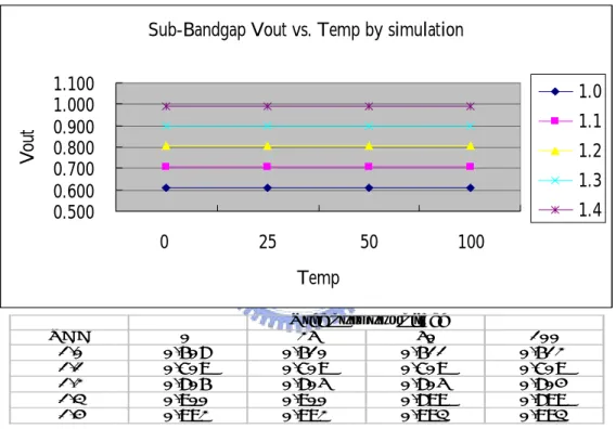
2.4 Cur re nt Mir ro r in the a m plif ie rFig 2.5 shows the simulation result that the temperature coefficient is 40ppm/°C. The sub-bandgap chip is simulated by HSPICE. Post-simulation is completed by HSPICE with spice model of TSMC 90nm 1P9M Low-Power process. The Vref voltage output is lower than supply voltage by 0.4V in each voltage step. When supply voltage vary from 1.4V to 1.0V, the bandgap output voltage change from 1.0V to 0.6V.
Sub-Bandgap Vout vs. Temp by simulation
0.500 0.600 0.700 0.800 0.900 1.000 1.100 0 25 50 100 Temp Vo ut 1.0 1.1 1.2 1.3 1.4 VDD 0 25 50 100 1.0 0.608 0.610 0.611 0.612 1.1 0.709 0.709 0.709 0.709 1.2 0.806 0.805 0.805 0.804 1.3 0.900 0.900 0.899 0.899 1.4 0.992 0.992 0.993 0.993
Vref outp ut voltage
2.4 SUB-BANDGAP CIRCUIT REALIZATION
The designed sub-bandgap circuit has been implemented on a test chip, which includes SRAM macros and this sub-bandgap circuit and manufactured in TSMC 90nm Low Power process technology. The pins out related to sub-bandgap are isolated power pins (VDD and VSS) and Vref output voltage.
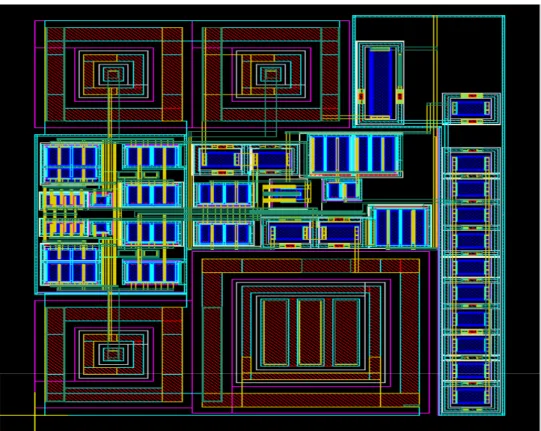
This sub-bandgap testchip can be divided in three parts. They are a Low Voltage amplifier, a sub-bandgap core with large resistor’s area, and bias circuit. The sub-bandgap layout and chip floorplan is shown in Fig 2.6. The die photograph is shown in Fig 2.7.
To avoid the substrate noise, the guard ring surrounds each MOS device to avoid the substrate noise and signal couple. It also used to prevent the latch-up issue caused by parasitic SCR circuit for large MOS devices. The dummy POLY and dummy OD are usually inserted to reduce the side effect of process etching and CMP. The dummy metal is added in the top of layout, the dummy metal occupies large area. It is used to improve the metal density and to overcome the DRC density violation. To improve the metal CMP process window, it must fill the dummy metal uniformly even if the originally drawn has already met the density rule. The dummy metal can be also worked as power line simultaneously.
The layout of BJT transistors is provided in TSMC SPICE package. There have 2um X 2um, 5um X 5um and 10um X 10um three kinds BJT layout with SPICE model from TSMC SPICE package. Meanwhile, the layout of POLY resistor is also provided from TSMC library. The BJT and resistors are silicon proven and the measurement data is collected in SPICE model document for our reference.
The chip floorplan must consider the optimum signal flow path. It should be as short as possible in metal routing and alleviate mismatch effect (loading balance) in low voltage amplifier. The low voltage amplifier placed on the center of chip and drew in finger type, which surrounded by guard ring, to make the differential input in balance. Whole circuitry is layout by single POLY and three metal layers, since 90nm process technology provided 1P9M process layers. All metal layers above metal3 are repeated up to metal9 with dummy metals. The whole chip area is 48um X 60um, which is 0.00288mm2.
Fig 2.7 1V Sub-band gap circuit’s silicon
Micrograph of Sub-Bandgap
48um60
um
Area = 0.00288mm2Micrograph of Sub-Bandgap
48um60
um
Area = 0.00288mm22.5 MEASUREMENT RESULT
The sub-bandgap chip is measured by memory tester 5335P and thermal stream machine, which provide stable temperature environment. The measurement data is shown in Fig. 2.8. Tester 5335P provide the power supply and measure the Vref output voltage at temperature 0°C, 25°C, 50°C and 100°C. Compared to post-simulation data, the measured data is not correlated to simulation data, especially at high temperature. The HSPICE. Post-simulation is completed by HSPICE with spice model of TSMC 90nm 1P9M logic process.
The sub-bandgap testchip has several components totally consumes about 1.575-mW DC power. In power domain, the measurement data is slightly greater than the post-simulation results.
Sub-Bandgap Vout vs. Temp
0.500
0.600
0.700
0.800
0.900
1.000
1.100
0
25
50
100
Temp
Vo
ut
1.0
1.1
1.2
1.3
1.4
VDD 0 25 50 100 1.0 0.624 0.606 0.593 0.556 1.1 0.725 0.709 0.692 0.658 1.2 0.818 0.805 0.788 0.753 1.3 0.912 0.899 0.884 0.850 1.4 1.008 0.993 0.978 0.940Vref outp ut voltage
Fig 2.8 The measurement results of 1-V sub-bandgap circuit
2.6 EXPLANATION OF SIMULATION AND MEASUREMENT’S
DISCRIPANCY
There exists discrepancy between simulation and silicon measurement data, and we need to find out the root cause to correct the simulation. Please refer to Fig 2.9, the difference of temperature coefficient at VDD=1.2V is 630ppm/ °C. After checking the simulation log file (Fig 2.10), the BJT Q0 and Q1 are in cut off state, because R2A (R2A1+R2A2=1000ohm) and R2B (R2B1+R2B2=1000ohm) resistance both are too low. The Ids of P21 and P22 are 300µA, therefore, emitter voltage of Q0 and Q1 are at 300mv which can’t turn on the BJT Q0 and Q1’s junction. Both BJT’s emitter current are at ~100fA, which proves both Q0 and Q1
are in cut off state. The behavior of Q0 and Q1 plays like a 3E12 ohm high resistance. simulation vs. measurement 0.500 0.600 0.700 0.800 0.900 1.000 1.100 0C 25C 50C 100C Temp Vo ut ( V) 1.0V-simu 1.0V-meas 1.1V-simu 1.1V-meas 1.2V-simu 1.2V-meas 1.3V-simu 1.3V-meas 1.4V-simu 1.4V-meas
Fig 2.9 The comparison between simulation and measurement
**** bipolar junction transistors
subckt xvref xvref xvref xvref element 1:q0 1:q1 1:q2 1:q3 model 0:pnp2 0:pnp2 0:pnp2 0:pnp2 ib -76.4173f -229.2520f -16.9183u -16.9246u ic -32.8884f -98.6651f -17.3771u -17.3836u vbe -301.1851m -301.1851m -834.7032m -834.7141m vce -301.1851m -301.1851m -1.1319 -1.1319 vbc 0. 0. 297.1514m 297.1696m vs -353.4894f -353.4894f -186.7722u -186.8416u power 32.9213f 98.7638f 33.7902u 33.8034u betad 430.3783m 430.3783m 1.0271 1.0271 gm 1.2451p 3.7354p 651.9304u 652.1705u rpi 371.8784g 123.9595g 1.5928k 1.5922k rx 126.0000 42.0000 121.3462 121.3446 ro 2.247e+16 7.493e+15 61.2139x 61.1912x cpi 6.1237f 18.3711f 7.4117f 7.4117f cmu 39.1406f 117.4218f 33.9286f 33.9283f
The simulation data show BJT Q0 and and Q1’s emitter current is around ~100fA, and Vce is around 300mv, which indicated the Q0 and Q1 are in cut off state.
Fig 2.10 The BJT’s simulation log file
Because Q0 and Q1 are in cut off state, therefore, PTAT current is not formed. Instead, the current is formed by R2A and R2B resistors, which is flew through 300mA current individually. The current copy to output device P23 is not a PTAT current, but a current proportional to resistor’s temperature coefficient. Therefore, the output voltage is not following the bandgap’s voltage output equation any more, but following the resistor and MOS’s temperature coefficients.
Another reason make the discrepancy is the resistor model version was changed from V1.0 to V1.3 after test chip was taped out. In V1.0 resistor model, only temperature coefficients (TC1 and TC2) were provided. In V1.3 resistor model, the POLY resistor is not only modeled by TC1 and TC2, but also modeled in sub-circuit format, which is much more accuracy than V1.0’s. Please refer to Fig 2.11, which shows T.C. of V1.0 resistor model is +0.0036 /°C. Please refer to Fig 2.12, which shows the T.C. of V1.3 resistor model is –0.0025/°C. The Fig. 2.13 shows the drain current Ids of P23 vs. temperature by SPICE model V1.0 and V1.3 The Ids of P23 also has negative temperature coefficient, that is, the Ids is decreasing when temperature is raising. Because the Vref output voltage is the multiplication of Ids P23 and R3 resistance, therefore, in Fig. 2.14 it present the Vref output voltage is decreasing with temperature raised. This is caused by multiplication of two negative temperature coefficient devices P23 and R3. After using resistor model V1.3, the Fig 2.15 shows the simulation result is closer to silicon measurement data. The discrepancy between simulation and measurement is caused by the inaccuracy of resistance model V1.0. Meanwhile, the low resistance R2A and R2B, which make sub-bandgap circuit’s Q0 and Q1 in cut off state, cause the amplifier’s feedback loop is not formed and whole sub-bandgap circuit is not functional.
R(V1.0) vs. Temp 1500 1700 1900 2100 2300 0C 20C 40C 60C 80C 100C Temp R ( ohm ) 1.0V 1.1V 1.2V 1.3V 1.4V VDD 0C 10C 20C 30C 40C 50C 60C 70C 80C 90C 100C 1.0V 1664 1719 1772 1830 1885 1938 2000 2052 2111 2170 2228 1.1V 1665 1716 1771 1830 1885 1940 1997 2054 2111 2166 2223 1.2V 1663 1719 1771 1827 1884 1942 1997 2050 2109 2168 2225 1.3V 1664 1717 1775 1828 1883 1940 1995 2052 2112 2165 2226 1.4V 1664 1719 1771 1826 1884 1939 1998 2055 2110 2167 2223 Resistor by V 1.0 R model
Fig 2.11 Resistance vs. Temp. of V1.0 Resistor model
Resistor vs. temp 1520 1530 1540 1550 0C 20C 40C 60C 80C 100C Temp R (ohm ) 1.0V 1.1V 1.2V 1.3V 1.4V Resistance by V1.3 R Model VDD 0C 10C 20C 30C 40C 50C 60C 70C 80C 90C 100C 1.0V 1552 1547 1544 1540 1537 1534 1530 1529 1525 1524 1525 1.1V 1551 1546 1544 1534 1540 1534 1531 1530 1526 1524 1525 1.2V 1549 1546 1542 1540 1539 1534 1533 1528 1526 1525 1523 1.3V 1551 1547 1544 1541 1537 1533 1532 1530 1527 1526 1522 1.4V 1551 1546 1544 1540 1537 1533 1530 1529 1528 1525 1524
Id_mp23 by V1.0R model with V1.0/V1.3 BJT 200 300 400 500 600 700 0C 20C 40C 60C 80C 100C Temp Id + m p2 3 1.0V 1.1V 1.2V 1.3V 1.4V
Id_mp23 by V1.3 R model with V1.0/V1.3 BJT
200 300 400 500 600 700 0C 20C 40C 60C 80C 100C Temp Id _m p2 3 1.0V 1.1V 1.2V 1.3V 1.4V
Fig 2.13 The Ids of p23 versus Temp by model V1.0 and V1.3.
Vref simulation by new model
0.5 0.6 0.7 0.8 0.9 1 1.1 0C 10C 20C 30C 40C 50C 60C 70C 80C 90C 10 0C Temp Vo ut ( V) 1.0V 1.1V 1.2V 1.3V 1.4V
Vref output voltage by new model
VDD 0C 10C 20C 30C 40C 50C 60C 70C 80C 90C 100C 1.0V 0.632 0.622 0.613 0.604 0.595 0.586 0.577 0.568 0.56 0.551 0.543 1.1V 0.729 0.719 0.709 0.699 0.689 0.68 0.67 0.661 0.651 0.642 0.632 1.2V 0.823 0.812 0.802 0.792 0.781 0.771 0.761 0.751 0.741 0.731 0.721 1.3V 0.914 0.903 0.893 0.882 0.872 0.862 0.851 0.841 0.831 0.82 0.81 1.4V 1.004 0.993 0.982 0.971 0.961 0.95 0.94 0.929 0.919 0.908 0.897
simulation vs. measurement 0.500 0.600 0.700 0.800 0.900 1.000 1.100 0C 25C 50C 100C Temp V ou t (V ) 1.0V-simu 1.0V-meas 1.1V-simu 1.1V-meas 1.2V-simu 1.2V-meas 1.3V-simu 1.3V-meas 1.4V-simu 1.4V-meas
Vref output voltage (V) comparison
VDD 0C 25C 50C 100C 1.0V-simu 0.632 0.608 0.586 0.543 1.0V-meas 0.624 0.606 0.593 0.556 1.1V-simu 0.729 0.704 0.680 0.632 1.1V-meas 0.725 0.709 0.692 0.658 1.2V-simu 0.823 0.797 0.771 0.721 1.2V-meas 0.818 0.805 0.788 0.753 1.3V-simu 0.914 0.887 0.862 0.810 1.3V-meas 0.912 0.899 0.884 0.850 1.4V-simu 1.004 0.976 0.950 0.897 1.4V-meas 1.008 0.993 0.978 0.940
CHAPTER 3
CIRCUIT ENHANCEMENT AND
SIMULATION RESULTS
This chapter presents the circuit enhancements and simulation results, which correct the test chip’s malfunctions and improve VDDmin performance. There exist several design issues in Fig 2.3 circuit. We correct the bias circuit, amplifier’s circuit, bandgap core circuit and add in start up circuit to make sure the sub-bandgap circuit is functional at low voltage. Meanwhile, we present one new scheme, which is by adding one DC bias voltage to improve VDDmin capability.
3.1 BIAS CIRCUIT ENHANCEMENT
The bias circuit shown in Fig 2.3 is independent of OPAMP’s operation. The bias circuit needed to be controlled by OPAMP’s output, which provides a feedback path to bias voltage generator. The OPAMP’s in Fig 2.3 works as an open loop OPAMP, because the output of differential amplifier is disconnected with the bias circuit. Therefore, modify the bias circuit’s connection as shown in Fig. 3.1.
Fig 3.1 The bias circuit correc
tion of 1-V sub-bandgap circuit
R3 P3 6 P3 7 P19 VO UT 40 /1 20 /1 40/ 1 40 /1 Q1 Q0 2000 R2A2 3000 1000 500 R2 A1 R1 10 2 10/ 1 1000 3000 P2 3 P2 1 P2 2 10/ 1 12 /1 4/ 1 4/ 0. 6 4/ 0. 6 20/ 1 MP A 04 MP A 02 P1 3 P1 4 MN 11 MN 12 2/ 2 2/ 2 MN A 00 MN A 03 4/ 1 1/ 1 C1 10 0f R2B1 R2B2 N3 5 N 34 di ffo ut qe0 qe1 rdivide1 di ff pl us di ff m inus di ff bi as 1 diffcs1 cs 1b cs 1a biasp2 biasp1 20 /1 R3 P3 6 P3 7 P19 VO UT 40 /1 20 /1 40/ 1 40 /1 Q1 Q0 2000 R2A2 3000 1000 500 R2 A1 R1 10 2 10/ 1 1000 3000 P2 3 P2 1 P2 2 10/ 1 12 /1 4/ 1 4/ 0. 6 4/ 0. 6 20/ 1 MP A 04 MP A 02 P1 3 P1 4 MN 11 MN 12 2/ 2 2/ 2 MN A 00 MN A 03 4/ 1 1/ 1 C1 10 0f R2B1 R2B2 N3 5 N 34 di ffo ut qe0 qe1 rdivide1 di ff pl us di ff m inus di ff bi as 1 diffcs1 cs 1b cs 1a biasp2 asp1 bi 20 /1
3.2 LOW VOLTAGE OPAMP’s ENHANCEMENT
After modify the bias circuit as shown in Fig. 3.1, the simulation shows MN11 and MN12 both NMOS are always in linear region. The reason is Q2 and Q3 work as DC level shifter, and make gate voltage of MN11 and MN12 are high enough to make their VDS voltage always higher than Vthn. Therefore, to make MN11 and MN12 both transistors in saturation region, we eliminate Q2 and Q3 and make the connections as shown in Fig. 3.2.
Fig 3.2 The enhanced low voltage OPAMP.
R3 P3 6 P3 7 P1 9 VO UT 40 /1 20 /1 40/ 1 40 /1 Q1 Q0 2000 R2A2 3000 1000 500 R2 A 1 R1 10 2 10 /1 1000 3000 P2 3 P2 1 P22 10/ 1 12/ 1 4/ 1 4/ 0. 6 4/ 0. 6 20 /1 MP A 04 MP A 02 P1 3 P14 MN 11 MN 12 2/ 2 2/ 2 MN A 00 MN A 03 4/ 1 1/ 1 C1 100 f R2B1 R2B2 N3 5 N 34 di ff o ut qe0 qe1 rdivide1 di ffp lu s di ff m inu s di ff b ias 1 diffcs1 cs 1b cs 1a biasp2 biasp1 20 /1 R3 P3 6 P3 7 P1 9 VO UT 40 /1 20 /1 40/ 1 40 /1 Q1 Q0 2000 R2A2 3000 1000 500 R2 A 1 R1 10 2 10 /1 1000 3000 P2 3 P2 1 P22 10/ 1 12/ 1 4/ 1 4/ 0. 6 4/ 0. 6 20 /1 MP A 04 MP A 02 P1 3 P14 MN 11 MN 12 2/ 2 2/ 2 MN A 00 MN A 03 4/ 1 1/ 1 C1 100 f R2B1 R2B2 N3 5 N 34 di ff o ut qe0 qe1 rdivide1 di ffp lu s di ff m inu s di ff b ias 1 diffcs1 cs 1b cs 1a biasp2 biasp1 20 /1
To make sure the Low Voltage amplifier’s gain is high enough to make the Va and Vb in bandgap core, we do the gain analysis as below.
Fig 3.3 The LV amplifier
VDD = 1.2V P19 20/1 4/1 4/0.6 4/0.6 20/1 MPA04 MPA02 P13 P14 MN11 MN12 2/2 2/2 MNA00 MNA03 4/1 diffplus diffminus diffbias1 diffc s1 cs1b cs1a 20/1 diffout biasp2 VDD = 1.2V P19 20/1 4/1 4/0.6 4/0.6 20/1 MPA04 MPA02 P13 P14 MN11 MN12 2/2 2/2 MNA00 MNA03 4/1 diffplus diffminus diffbias1 diffc s1 cs1b cs1a 20/1 diffout biasp2
The first stage gain, as listed in Eq. (16), of Low Voltage amplifier is around 1, which is quite small. The second stage gain, as listed in Eq. (17), is around 40dB (~100). (16)
1
V
V
A
T 12 12 T 14 14 12 14 0 = =≅
n
I
n
I
g
g
D D m m v(17) T 13 4 3 11 3 4 3 11 3 13 0
V
)
(
)
/S
(S
)
/
(
A
n
g
g
S
S
g
ds ds m vλ
λ
+
+
= =3.3 START UP CIRCUIT FOR LOW VOLTAGE OPERATION
When lower voltage to 1.15V, some MOSFET in Fig 3.1 become cut-off, and bandgap circuit is not functional any more. We have current mirror type current source to provide bias voltage to amplifier. The operation point in current mirror type current source exist two stable positions, which indicated in Fig 3.4. After added in start up circuit likes in Fig 3.5 and Fig 3.6, the start up circuit will sense the amplifier’s output voltage. If the amplifier’s output voltage is approach zero voltage, then start up circuit will inject current to current mirror type current source to bring the operation point from zero voltage stable operation point to another operation point, which amplifier will be functional and output the corrected voltage. In turn, this corrected voltage output will turn off the start up circuit to disable the interruption from start up circuit to current mirror type current source.
I
D 2 THS GS1 D1(
V
V
)
2
β
I
=
−
2 THS GS2 D2(
V
V
)
2
β
I
=
−
I
D 2 THS GS1 D1(
V
V
)
2
β
I
=
−
2 THS GS2 D2(
V
V
)
2
β
I
=
−
Fig 3.4 The operation point of current source
Vref
Q1
Q2
R1
R2A2 M1 R3 Bias CKT Start up CKT LV OPA R2A1 R2B1 R2B2 M2 M3Bandgap
Core
Vref
Q1
Q2
R1
R2A2 M1 R3 Bias CKT Start up CKT LV OPA R2A1 R2B1 R2B2 M2 M3Bandgap
Core
Fig 3.6 The 1-V sub-bandgap circ
uit with start up circuit
R3 P3 6 P37 P19 VO U T 4/ 1 20 /1 4/ 1 4/ 1 Q1 Q0 200K R2A2 300K 100K 30K R2 A 1 R1 10 2 10 /1 100K 300K P2 3 P2 1 P22 10 /1 12 /1 4/ 1 4/ 0.6 4/ 0.6 20 /1 MP A 04 MP A 02 P1 3 P1 4 MN 11 MN 12 2/ 2 2/ 2 MN A 00 MN A 03 4/ 1 1/ 1 C1 10 0f R2B1 R2B2 N3 5 N3 4 di ff o ut qe0 qe1 rdivide1 di ff p lu s di ff m in us di ff b ias 1 VD D diffcs1 cs 1b cs 1a biasp2 biasp1 20 /1 P2 4 8/ 4 P2 5 1/ 4 N26 1/ 6 R3 P3 6 P37 P19 VO U T 4/ 1 20 /1 4/ 1 4/ 1 Q1 Q0 200K R2A2 300K 100K 30K R2 A 1 R1 10 2 10 /1 100K 300K P2 3 P2 1 P22 10 /1 12 /1 4/ 1 4/ 0.6 4/ 0.6 20 /1 MP A 04 MP A 02 P1 3 P1 4 MN 11 MN 12 2/ 2 2/ 2 MN A 00 MN A 03 4/ 1 1/ 1 C1 10 0f R2B1 R2B2 N3 5 N3 4 di ff o ut qe0 qe1 rdivide1 di ff p lu s di ff m in us di ff b ias 1 VD D diffcs1 cs 1b cs 1a biasp2 biasp1 20 /1 P2 4 8/ 4 P2 5 1/ 4 N26 1/ 6
3.4 SIMULATION RESULTS OF ENHANCED CIRCUIT
Before we run simulation for new revision sub-bandgap circuit, we need to make sure the BJT Q0 and Q1 are both in active state to avoid the last version design issue. We raise the resistor R1, R2A1, R2A2, R2B1, R2B2 and R3’s resistance value to several hundreds kilo ohm to make sure the qe0 and qe1 voltage level won’t bring down by resistive division circuit. In Fig 3.7 the simulation log file shows both BJT Q0 and Q1’s Vbe is 640mv and collector current is around 0.7uA, therefore, we confirm that both BJT Q0 and Q1 are in active state. In Fig 3.8, the revised sub-bandgap circuit simulation shows the circuit’s VDDmin can achieve 0.85V with temperature coefficient 60ppm/°C. The VDDmin of revised sub-bandgap circuit is limited by qe0 and qe1’s voltage level. When power supply voltage decrease from 1.0V to 0.85V, the qe0 and qe1 voltage are kept at around 0.64V, which is BJT’s Vbe junction voltage. Because qe0 and qe1 are kept at 0.64V, the input devices of amplifier P13 and P14 will be cut off when VDD is lowered to 0.85V. The Vbe junction voltage is determined by process technology, this means the limit of VDDmin of existing circuit is around 0.85V. To improve the low voltage operation limits, we need new circuit scheme to enhance the VDDmin performance of this revised sub-bandgap circuit.
3.5 THE NEW SCHEME TO ENHANCE VDDmin PEFORMANCE
To enhance the VDDmin performance of the revised sub-bandgap circuit, we propose to add one negative DC bias voltage between BJT Q0 and Q1’s base and collector. Please refer to Fig 3.9. By this way, we decrease the voltage level at qe0 and qe1 branch, but still keep BJT’s Vbe voltage drop between BJT’s
base and emitter terminals. For example, by adding negative DC bias –100mv between base and collector of BJT Q0 and Q1, then the qe0 and qe1 will be drop 100mv accordingly, but BJT’s Vbe junction voltage kept at same voltage level. The equation (14) in chapter 2 remains valid in this scheme. Please refer to Fig 3.10, after adding the negative bias –100mv, the qe0 shift down 100mv accordingly. With this new scheme, we re-run the simulation and the data show the VDDmin is improved to 0.8V with temperature coefficient 60ppm/°C. Please refer to Fig. 3.11. The VDDmin improvement is from the headroom of input devices P13 and P14 of amplifier gain the same voltage level as added DC bias voltage level, therefore, the P13 and P14 were not in cut off region when VDD lower to 0.8V. The maximum negative DC bias can’t be greater than –0.3V, otherwise the junction between base and collector of BJT will be turn on. Theoretically, the VDDmin of sub-bandgap voltage can be lower than 0.7V, which is at the same VDDmin level of logic circuit, and this help us to integrate digital circuit with sub-bandgap circuit use single power supply.
**** bipolar junction transistors subckt xvref xvref
element 1:q0 1:q1 model 0:pnp10 0:pnp10 ib -718.3792n -719.9735n ic -749.8297n -742.1432n vbe -640.1675m -598.3004m vce -640.1675m -598.3004m vbc 0. 0. vs -2.2307u -441.5752n power 939.8997n 874.7851n betad 1.0438 1.0308 gm 29.0244u 28.7305u rpi 36.2142k 36.1835k rx 42.2137 8.4485 ro 1.1649g 1.1776g cpi 299.8605f 1.4774p cmu 180.8571f 940.2971f
The simulation data show BJT Q0 and and Q1’s emitter current is around ~0.7uA, and Vce is around 640mv, which indicated the Q0 and Q1 are in active state.
Vref vs. Temp 0.580.6 0.62 0.64 0.66 0.68 0C 20C 40C 60C 80C 100C Temp Vr ef (V ) 1.0V 0.95V 0.9V 0.85V 0.8V 0.75V 0.7V
Vref output with Temp.
VDD 0C 10C 20C 30C 40C 50C 60C 70C 80C 90C 100C 1.0V 0.618 0.617 0.616 0.615 0.614 0.614 0.614 0.615 0.616 0.618 0.621 0.95V 0.617 0.616 0.614 0.613 0.612 0.612 0.612 0.612 0.612 0.614 0.616 0.9V 0.617 0.615 0.613 0.612 0.611 0.61 0.609 0.609 0.609 0.61 0.612 0.85V 0.619 0.615 0.613 0.61 0.609 0.607 0.606 0.605 0.605 0.606 0.607 0.8V 0.629 0.62 0.614 0.61 0.607 0.604 0.602 0.601 0.6 0.6 0.6 0.75V 0.66 0.638 0.622 0.611 0.604 0.6 0.597 0.594 0.593 0.591 0.591 0.7V 0.66 0.651 0.634 0.617 0.603 0.593 0.587 0.582 0.579 0.577 0.576
R3 P36 P37 P1 9 VO UT 4/ 1 20/ 1 4/ 1 4/ 1 Q1 Q0 200K R2A2 300K 100K 30K R2 A 1 R1 10 2 10/ 1 100K 300K P23 P21 P22 10/ 1 12/ 1 4/ 1 4/ 0.6 4/ 0.6 20/ 1 MP A 04 MP A 02 P13 P 14 MN 11 MN 12 2/ 2 2/ 2 MN A 00 MN A 03 4/ 1 1/ 1 C1 100f R2B1 R2B2 N3 5 N3 4 di ff o ut qe0 qe1 rdivide1 di ffp lu s di ff m inus di ff b ias 1 diffcs1 cs 1b cs 1a biasp2 biasp1 20/ 1 P2 4 8/ 4 P25 1/4 N2 6 1/ 6 R3 P36 P37 P1 9 VO UT 4/ 1 20/ 1 4/ 1 4/ 1 Q1 Q0 200K R2A2 300K 100K 30K R2 A 1 R1 10 2 10/ 1 100K 300K P23 P21 P22 10/ 1 12/ 1 4/ 1 4/ 0.6 4/ 0.6 20/ 1 MP A 04 MP A 02 P13 P 14 MN 11 MN 12 2/ 2 2/ 2 MN A 00 MN A 03 4/ 1 1/ 1 C1 100f R2B1 R2B2 N3 5 N3 4 di ff o ut qe0 qe1 rdivide1 di ffp lu s di ff m inus di ff b ias 1 diffcs1 cs 1b cs 1a biasp2 biasp1 20/ 1 P2 4 8/ 4 P25 1/4 N2 6 1/ 6 R3 P36 P37 P1 9 VO UT 4/ 1 20/ 1 4/ 1 4/ 1 Q1 Q0 200K R2A2 300K 100K 30K R2 A 1 R1 10 2 10/ 1 100K 300K P23 P21 P22 10/ 1 12/ 1 4/ 1 4/ 0.6 4/ 0.6 20/ 1 MP A 04 MP A 02 P13 P 14 MN 11 MN 12 2/ 2 2/ 2 MN A 00 MN A 03 4/ 1 1/ 1 C1 100f R2B1 R2B2 N3 5 N3 4 di ff o ut qe0 qe1 rdivide1 di ffp lu s di ff m inus di ff b ias 1 diffcs1 cs 1b cs 1a biasp2 biasp1 20/ 1 P2 4 8/ 4 P25 1/4 N2 6 1/ 6 R3 P36 P37 P1 9 VO UT 4/ 1 20/ 1 4/ 1 4/ 1 Q1 Q0 200K R2A2 300K 100K 30K R2 A 1 R1 10 2 10/ 1 100K 300K P23 P21 P22 10/ 1 12/ 1 4/ 1 4/ 0.6 4/ 0.6 20/ 1 MP A 04 MP A 02 P13 P 14 MN 11 MN 12 2/ 2 2/ 2 MN A 00 MN A 03 4/ 1 1/ 1 C1 100f R2B1 R2B2 N3 5 N3 4 di ff o ut qe0 qe1 rdivide1 di ffp lu s di ff m inus di ff b ias 1 diffcs1 cs 1b cs 1a biasp2 biasp1 20/ 1 P2 4 8/ 4 P25 1/4 N2 6 1/ 6
Vbe vs wo bias & wi bias 0.35 0.45 0.55 0.65 0.75 0C 20C 40C 60C 80C 100C Temp Vb e (V ) qe0-90TT qe0-bias
Vbe voltage shift with/without DC bias
qe0-90TT 0.701 0.682 0.663 0.644 0.625 0.605 0.586 0.566 0.547 0.527 0.507 qe0-bias 0.59 0.57 0.55 0.531 0.511 0.491 0.472 0.452 0.432 0.412 0.392
Fig 3.10 The Vbe voltage shift with/without DC bias
Vref with bias vs. Temp
0.537 0.557 0.577 0C 20C 40C 60C 80C 100 C Temp V re f(V ) 1.0V 0.95V 0.9V 0.85V 0.8V 0.75V 0.7V
Vref output voltage with bias vs. Temp.
VDD 0C 10C 20C 30C 40C 50C 60C 70C 80C 90C 100C 1.0V 0.563 0.563 0.562 0.561 0.561 0.561 0.562 0.563 0.565 0.568 0.572 0.95V 0.562 0.561 0.56 0.56 0.559 0.559 0.559 0.56 0.561 0.564 0.567 0.9V 0.561 0.56 0.559 0.558 0.557 0.557 0.557 0.557 0.558 0.56 0.562 0.85V 0.56 0.558 0.557 0.556 0.555 0.554 0.554 0.554 0.554 0.556 0.557 0.8V 0.558 0.557 0.555 0.554 0.553 0.552 0.551 0.551 0.551 0.551 0.552 0.75V 0.557 0.555 0.553 0.551 0.549 0.548 0.547 0.546 0.546 0.546 0.546 0.7V 0.559 0.553 0.549 0.546 0.544 0.542 0.54 0.539 0.538 0.538 0.537
CHAPTER 4
CONCLUSIONS AND FUTURE WORKS
4.1 CONCLUSIONS
The Low Voltage sub-bandgap voltage reference generator without special device is designed, fabricated, measured and enhanced. The sub-bandgap testchip comprised Low Voltage amplifier, bias circuit, and bandgap core circuit. The sub-bandgap testchip is fabricated by TSMC 90nm logic process and measurement results have been presented in this thesis. Although the performance didn’t meet design specifications and discrepancy exist between simulation and measurement, but we find out the root cause of discrepancy and new simulation result proves the simulation data close to measurement data.
After fix the simulation discrepancy, we enhance the sub-bandgap circuit by modify bias generator with a feedback control, eliminate the DC level shifter and all MOS in low voltage amplifier can be in saturation region, add in the start up circuit and circuit can operate down to sub-1-V voltage range. With all these enhancements, the sub-bandgap circuit can operate around VDD is 0.9V – 0.85V. To improve VDDmin performance further, a new scheme with DC bias adding between base and collector terminal of BJT is proposed. The VDDmin can be improved down to 0.8V with temperature coefficient 60ppm/°C. The performance of VDDmin (0.8V) of this sub-bandgap circuit is the lowest VDD capability, comparing to other published works. Please refer to table 1, the voltage difference between VDDmin and voltage output (120mv) is also the lowest voltage difference, comparing to existing published works.
Technology Threshold Voltage Min VDD Isb Vref TC This work 90 nm CMOS Vthp= -0.22 V Vthn= +0.31V 0.80V 44uA 0.620 mV 60 ppm/C (simulation) Leung st.al. 0.6 um CMOS Vthp= -0.9 V Vthn= +0.9V 0.98 V 18 uA 603 mV 15 ppm/C Jiang et al. 1.2 um CMOS Vthp= -0.91 V Vthn= +0.53V 1.2 V 500 uA 1000 mV +- 100 ppm/C (not trimmed) Annema 0.35 um CMOS Vthp= -0.65 V Vthn= +0.65V 0.85 V < 1.2 uA 650 mV 57 ppm/C Banba et al. 0.35 um CMOS Vthp= -0.65 V Vthn= +0.65V 0.85 V < 1.2 uA 650 mV 57 ppm/C Malcovati et al. 0.8 um BiCMOS -0.95 V < 92uA 536 mV 19 ppm/C (VDDmin – Vref) 120 mV 377 mV 200 mV 200 mV 200 mV 414 mV Technology Threshold Voltage Min VDD Isb Vref TC This work 90 nm CMOS Vthp= -0.22 V Vthn= +0.31V 0.80V 44uA 0.620 mV 60 ppm/C (simulation) Leung st.al. 0.6 um CMOS Vthp= -0.9 V Vthn= +0.9V 0.98 V 18 uA 603 mV 15 ppm/C Jiang et al. 1.2 um CMOS Vthp= -0.91 V Vthn= +0.53V 1.2 V 500 uA 1000 mV +- 100 ppm/C (not trimmed) Annema 0.35 um CMOS Vthp= -0.65 V Vthn= +0.65V 0.85 V < 1.2 uA 650 mV 57 ppm/C Banba et al. 0.35 um CMOS Vthp= -0.65 V Vthn= +0.65V 0.85 V < 1.2 uA 650 mV 57 ppm/C Malcovati et al. 0.8 um BiCMOS -0.95 V < 92uA 536 mV 19 ppm/C (VDDmin – Vref) 120 mV 377 mV 200 mV 200 mV 200 mV 414 mV
4.2 FUTURE WORKS
A 1-V sub-bandgap voltage reference generator is fabricated with several important key components. They are a Low Voltage amplifier, a bandgap core and bias circuit. After circuit enhancement, the VDDmin can be achieved 0.8V without scarifying temperature coefficient (60ppm/°C). For future work, a better temperature coefficient > 1ppm/°C should be achieved for precision analog system applications.
A sub-bandgap core circuit is implemented with resistive division scheme to lower the Vref output voltage, but the resistor with several hundred K resistance is too high and will occupy big area.. For future work, it can be researched that the other scheme can also be implement to further reduction the resistor area, or even a low voltage sub-bandgap circuit without resistors.
The Vbe of BJT remains the same voltage level even process technology advances one generation every 18 months. In the sub-nanometer process technology, the VDDmin performance of sub-bandgap circuit won’t limit by Vt of MOS devices, but limit by Vbe of BJT device. Even with DC bias scheme proposed in this thesis to lower Vbe voltage, we don’t eliminate the Vbe limitation totally. Therefore, it is challenge to design sub-bandgap circuit at low voltage operation.
In the deep sub-micron technology, like 90nm process technology, the mismatch effect becomes more severe than previous generation. To layout the differential pair or BJT in symmetrical style is not enough for devices matching. The dummy pattern or OPC compensation becomes more important than old technology. The RC-extraction EDA tools to calculate the parasitic RC and added
into circuit simulation is much more important than before. The parasitic RC of dummy metal, dummy POLY..etc are needed to be considered.
REFERENCES
[1] Phillip E. Allen and Douglas R. Holberg, CMOS Analog Circuit Design. Oxford University Press.
[2] Behzad Razavi, RF Microelectronics. Prentice Hall
[3] A.P. Brokaw, “A Simple Three-Terminal IC Bandgap Reference” IEEE Journal of Solid-State Circuits, vol. SC-9, pp388-393, Dec. 1974.
[4] D. Johns and K. Martin, Analog Integrated Circuit Design, Wiley 1997.
[5] H. Banba, H. Shiga, A. Umezawa, T. Tanzawa, S. Atsumi and K. Sakui, “A CMOS Bandgap Reference Circuit with Sub-1-V Operation” IEEE Journal of Solid-State Circuits, vol. 34, pp. 670-674, May 1999.
[6] K.N. Leung and P.K.T. Mok, “A Sub-1-V 15-ppm/°C CMOS Bandgap Voltage Reference without requiring Low Threshold Voltage Device” IEEE Journal of Solid-State Circuits, vol. 37, pp.526-530, Apr. 2002.
[7] Y. Jiang and E.K.F. Lee, “Design of Low-Voltage Bandgap Reference Using Transimpedance Amplifier” IEEE Transaction on Circuits and System II, vol. 47, pp.552-555, Jun. 2000.
[8] B. S. Song and P. R. Gray, “A Precision Curvature-Compensated CMOS Bandgap Reference” IEEE Journal of Solid-State Circuits, vol. SC-18, pp.634-643, Dec. 1983.
[9] P. Malcovati, F. Maloberti, C. Fiocchi and M. Pruzzi, “A New Curvature Corrected Bandgap reference” IEEE Journal of Soild-State Circuits, vol.36, pp.1076-1081, July 2001.
[10] K.N. Leung, P.K.T. Mok and C.Y. Leung, “A 2-V 23-uA 5.3-ppm/°C Curvature Compensated CMOS Bandgap Reference” IEEE Journal of Solid-State Circuits, vol. 38, No.3 pp.561-564, Mar. 2003.
[11] K.N. Leung and P.K.T. Mok, “A CMOS Voltage Reference Based on Weighted ∆Vgs for CMOS Low-Dropout Linear Regulators” IEEE Journal of Solid-State Circuits, vol. 38, pp.146-150, Jan. 2003.
[12] K.N. Leung, P.K.T. Mok and K.C. Kwok, “CMOS Voltage Reference” US Patent 6,441,680, Aug.27, 2002.