國立交通大學
電子工程學系電子研究所
博士論文
低功耗前瞻靜態隨機記憶體之測試方法與錯誤模型
Test methodology and fault modeling for
low-power advanced SRAM
研究生:林政偉
指導教授:趙家佐
測
低功耗前瞻靜態隨機記憶體之測試方法與錯誤模型
Test methodology and fault modeling for
low-power advanced SRAM
研究生:林政偉
Student:Chen-Wei Lin
_____
指導教授:趙家佐 Advisor:Mango Chia-Tso Chao
國立交通大學
電機學院 電子工程學系 電子研究所
博士論文
A Dissertation
Submitted to Department of Electronics Engineering and Institute of Electronics
College of Electrical and Computer Engineering National Chiao-Tung University
in partial Fulfillment of the Requirements for the Degree of
Doctor of Philosophy
in
Electronics Engineering August 2013
Hsinchu, Taiwan, Republic of China
低功耗前瞻靜態隨機記憶體之測試方法與錯誤模型
研究生:林政偉 指導教授:趙家佐
國立交通大學
電機學院 電子工程學系 電子研究所
摘要
對於新開發的低功耗和前瞻靜態隨機存記憶體(SRAM),製造缺陷在其上 所造成的錯誤行為往往比對於在傳統 SRAM 上造成之錯誤行為來說較為複雜。 在相關的研究並未被充分的討論的情況下,許多針對傳統 6T SRAM 之一般 性的測試方式都未被驗證,也因此無法滿足對於在製造與設計堅固和可靠 的低功耗 SRAM 與未來的製程技術配合的測試需要。在這篇論文中,我討論 了對於各種已在科技文獻中發表的低功耗 SRAM 設計的測試。針對不同的記 憶胞結構我進行了分類並分析相對應的錯誤行為,並開發至少四個可以處 理的不同的低功耗 SRAM 測試需要的測試方法。除了討論各種記憶胞結構, 我也延伸了從傳統的平面 CMOS 元件的討論,到目前極具前瞻性的 FinFET 元件,以及特殊的薄膜電晶體元件。對於該些前瞻的 SRAM,我進行了元件 等級的 TCAD 模擬、SPICE 模型提取和針對多晶矽通道模型建立之應用等, 以進行驗證所提出的測試方法與最佳化前瞻 SRAM 設計的相關參數。Test methodology and fault modeling for
low-power advanced SRAM
Student:Chen-Wei Lin
Advisor:Mango Chia-Tso Chao
Department of Electronics Engineering
and Institute of Electronics
National Chiao-Tung University
Abstract
For the new-developed low-power and advanced SRAMs, the fault behaviors due to manufacture defects are often relatively complicated when being compared to the traditional 6T SRAM. And the complete analysis has not been fully discussed. As a result, the test effectiveness of conventional test methods for the 6T SRAM may not satisfy the need for producing robust and reliable low-power SRAMs with future technologies.
In this thesis, I have discussed the testing of various low-power SRAM designs which have been published in literatures. By categorizing the different cell structures and analyzing the corresponding faulty behaviors, I have developed at least four new test methods which can deal with the diverse needs of the low-power SRAM testing. In addition to including the various cell structures, I also extend the discussion to the SRAM which comes with the specific peripheral write-assist circuitry. For the data-aware write-assist SRAM,
a high-fault-coverage and time-efficient test method is proposed. Finally, the discussions of the special Gate-Oxide Short defects at the traditional planar bulk CMOS and the promising FinFET technology are also covered. For those advanced SRAMs, device-level TCAD simulation, SPICE model extraction, and circuit-level defect model establishing were proceeded to either verify the proposed test methods or to achieve high yield optimized advanced SRAM designing.
Acknowledgements
First and foremost, I would like to express my greatest appreciation to my advisor, Professor Chia-Tso Chao (Mango, 趙家佐) for his suggestions and guidance. He is extremely patient to me in everything no matter for the research discussion or life planning. I also would like to thank my labmates: Hung-Hsin Chen, Hao-Yu Yang, and Chin-Yuan Huang. They assist me in dealing with the weighty experiments and research tasks for the past five years.
Finally, I appreciate my parents and my wife for the constant comfort and encouragement.
Chen-Wei Lin
National Chiao-Tung University 2013, August
Contents
中文摘要 I English Abstract II Acknowledge IV List of Tables IX List of Figures XII
1 Introduction………1
2 Fault Models and Test Methods for Subthreshold SRAMs………3
2.1 Categorization of Subthreshold SRAM Designs……….5
2.2 Test Methods for Stability Faults……….6
2.2.1. Background of Stability Faults………....6
2.2.2. Read Equivalent Stress………7
2.2.3. Severe Write………7
2.2.4. High-V-Write/Low-V-Read……….9
2.3 Analysis of Open Defects in Type-A Subthreshold SRAMs…………9
2.3.1 Design Overview of Type-A Subthreshold SRAMs……9
2.3.2 Impact of Open Defects on Type-A Subthreshold SRAMs……….11
2.3.3 Effectiveness of Test Methods for Type-A Designs……13
2.4 Analysis of Open Defects in Type-B Subthreshold SRAMs………….14
2.4.1 Introduction of Type-B Subthreshold SRAMs…………14
2.4.2 Impact of Open Defects on Type-B Subthreshold SRAMs……….16
2.4.3 Effectiveness of Test Methods for Type-B Designs……17
2.5.1 Introduction of Type-C Subthreshold SRAMs…………..19
2.5.2 Impact of Open Defects on Type-C Subthreshold SRAMs……….21
2.5.3 Effectiveness of Test Methods for Type-C Designs……22
2.6 Address Decoder Faults in Subthreshold SRAMS………24
2.6.1 Type-A Subthreshold SRAM………24
2.6.2 Type-B Subthreshold SRAM………26
2.6.3 Type-C Subthreshold SRAM………26
2.6.4 Address-Decoder Faults with Sequential Behavior……30
2.7 Fault Models for Sense Amplifier under Subthreshold Operations…30 2.7.1 Open Defects………30
2.7.2 Vth Mismatch……….31
2.8 Impact of Temperature at Test………34
2.9 Conclusion……….35
3 Testing of a Low-VMIN Data-Aware Dynamic-Supply 8T SRAM…………37
3.1 Preliminary of the Low-VMIN Date-Aware Dynamic-Supply 8T SRAM………39
3.2 Using March C- to Detect Open Defects in the Low-VMIN DADS 8T SRAM………41
3.3 Test Methods for the Open Defects at the Cross-Couple Inverters...44
3.3.1 Floating Bit-Line Attacking Method………...44
3.3.2 Proposed Method: Self-Loop Attacking Method………46
3.3.3 Test Methods Comparison………49
3.4 Testing for The Open Defects in the DADS Circuitry………50
3.5 Conclusion……….52 4 A Novel Circuit-level Model for Gate Oxide Short and its Testing Method in
SRAMs……….54
4.1 Experimental Setup for TCAD and HSPICE……...57
4.2 Previous Circuit-Level GOS Models………59
4.2.1 Bi-dimensional model………59
4.2.2 Nonlinear non-split model 1 - JET_03...60
4.2.3 Nonlinear non-split model 2 - IDT_09………62
4.3 Proposed GOS Model and The Comparison With Previous Works...64
4.3.1 Proposed GOS model………64
4.3.2 Simulation comparisons on DC characteristics………….66
4.3.3 Simulation comparisons on transient characteristics……67
4.3.4 Modeling GOS defects with different locations…………70
4.4 Testing GOS in SRAMs……….71
4.4.1 Previous test methods………72
4.4.2 Proposed DFT write operation………75
4.4.3 Detailed simulation result for detecting GOS…………76
4.4.4 Finding valid setting for CT and ΔV………78
4.4.5 Comparison with other GOS models in use………79
4.5 Implementation of The Proposed Test Method & Its Optimization…80 4.5.1 Implementation and area overhead of DfT………80
4.5.2 Optimum (CT, ΔV) for minimizing area overhead………82
4.5.3 Maximization of tolerable ΔV range against the process variation………84
4.6 Conclusion……….85
5 Investigation of Gate Oxide Short in FinFETs and the Test Methods for FinFET SRAMs………87
5.2 Experiment Setup………90
5.3 GOS Fault Behaviors in FINFETs………91
5.3.1 Tied-Gate FinFET………...91
5.3.2 Independent-Gate FinFET………...92
5.3.3 Short Summary………..95
5.4 Testing of GOS in FinFET SRAMs………95
5.4.1 Traditional Tests: March Test and IDDQ Test…………96
5.4.2 Proposed Test method for TG-FinFET based SRAM…...98
5.4.3 Proposed Test method for IG-FinFET based SRAM…100 5.5 Conclusion………103
6 Summary……….104
7 Future Work………105
Bibliography………..106
List of Tables
Table 2-I Categorization of subthreshold SRAM designs………....5 Table 2-II Faulty behavior of open defects on Type-A designs (Fig. 2-2, 2-3, 2-4)………..12 Table 2-III Effectiveness of test methods for detecting STFs in Type-A
designs……….13 Table 2-IV Effectiveness of test methods for detecting fail-to-write gate open
defects in Type-A designs………14 Table 2-V Faulty behavior of open defects on Type-B designs (Fig. 2-5,
2-6)………..17 Table 2-VI Effectiveness of test methods for detecting STFs in Type-B
designs……….18 Table 2-VII Effectiveness of test methods for detecting fail-to-write gate open
defects in Type-B designs………18 Table 2-VIII Impact of using different backgrounds when testing fail-to-read open defects in Type-B designs………19 Table 2-IX Faulty behavior of open defects on Type-C designs (Fig. 2-7, 2-8)………22 Table 2-X Effectiveness of test methods for detecting STFs in Type-C
designs………...22 Table 2-XI Impact of using different write voltages during LVW-HVR for
Type-C designs………...23 Table 2-XII Impact of using different backgrounds when testing fail-to-read open defects in Type-C designs………...23
Table 2-XIII Setting of WL1 and WL2 for Type-C design………27
Table 2-XIV Faulty behavior of address decoder faults on Type-C designs (Fig. 2-8)………..28
Table 2-XV Minimum detectable resistance for open defects on a differential sense amplifier………32
Table 2-XVI Minimum detectable resistance for open defects on a single-ended sense amplifier………32
Table 3-I Control Signals for the 8T SRAM cell………40
Table 3-II Test Results of March C- for Open Defects………41
Table 3-III Control Signals of the FBA Test Method………....45
Table 3-IV Test Results of the FBA Test Method………46
Table 3-V Final States of Defect-Free Cells and Test Results of Open Defects of SLA under Process Corner TT………48
Table 3-VI Final States of Defect-Free Cells under Various Process Corners..49
Table 3-VII Test Methods Comparison of Test Efficacy and Test Time………50
Table 3-VIII Test Results of SLA for Open Defects in The DADS Circuitry………...51
Table 3-IX Simulation Results of Testing the Defects at M11 and M12 but under FF Process Corner………...52
Table 4-I DC Characteristics and Parasitic Capacitances of a Defect-Free nMOS and pMOS………....57
Table 4-II DC Fitting Errors Resulting From Different GOS Models………67
Table 4-III Fitting Errors of An Inverter’s Delay Caused by Different GOS Models……….69
Table 4-IV IDVD Fitting Errors of GOS Models With Different Defect Locations……….71
Table 4-V Fitting Errors of Inverter’s Delay of GOS Models with Different Defect Locations………71 Table 4-VI Result of Applying March C- Test to Detect A GOS in 6T SRAM...72 Table 4-VII IDDQ Sensitivity Caused by A GOS Based on A 1.2V 32KX32
SRAM………73 Table 4-VIII Comparison Between The Two Test Configurations P1 & P2
Labeled in Figure 4-27………85 Table 5-I Comparison of GOS Fault Behaviors of Different Transistors…95 Table 5-II Experiment Results of Applying Operation Pairs to Detect GOS in FinFET SRAMs………...97 Table 5-III IDDQ Sensitivity of FinFET SRAMs with GOS (Array Size is
162Mb [5-5])………98 Table 5-IV Test Efficacy Comparison of The Methods To Detect The GOSs in IG-FinFET SRAM………103
List of Figures
Fig. 2-1 Illustration of severe write………8
Fig. 2-2 First Type-A subthreshold SRAM design [2-9]………10
Fig. 2-3 Second Type-A subthreshold SRAM design [2-10]………10
Fig. 2-4 Third Type-A subthreshold SRAM design [2-11]………11
Fig. 2-5 First Type-B subthreshold SRAM design [2-12]………15
Fig. 2-6 Second Type-B subthreshold SRAM design [2-13]………16
Fig. 2-7 First Type-C subthreshold SRAM design [2-14]………20
Fig. 2-8 Second Type-C subthreshold SRAM design [2-15]………21
Fig. 2-9 (a) Conventional march sequence for detecting ADFs; (b) Types of address decoder faults………24
Fig. 2-10 Schematics of single-ended and differential sense amplifiers……31
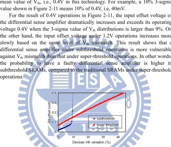
Fig. 2-11 99th percentile of the largest input voltage offset versus Vth mismatch for a differential SA operating at 0.4V and 1.2V, respectively………33
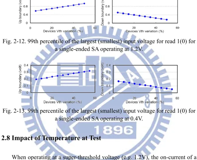
Fig. 2-12 99th percentile of the largest (smallest) input voltage for read 1(0) for a single-ended SA operating at 1.2V………34
Fig. 2-13 99th percentile of the largest (smallest) input voltage for read 1(0) for a single-ended SA operating at 0.4V………34
Fig. 2-14 (a) Cycle time versus temperature and (b) Power consumption versus temperature for a 128x32 subthreshold SRAM array………….35
Fig. 3-1 Schematic of the low-VMIN data-aware dynamic-supply 8T SRAM [3-7]………...39 Fig. 3-2 Illustration of how background cells affect the testing of the defect at
M6………..43 Fig. 3-3 An example of floating bit-line attacking method: using floating-0 on bit-line for detecting the open defects R1………45 Fig. 3-4 Configuration of the proposed self-loop attacking test method………47 Fig. 3-5 Valid SL range under different process corners………51 Fig. 4-1 Cross-section view of a GOS-impacted MOSFET………55 Fig. 4-2 IDVD curves of a nMOS (a) without and (b) with a gate-to-channel
GOS………...56 Fig. 4-3 Representation of a 3D GOS-impacted MOSFET in TCAD…………58 Fig. 4-4 Comparison of an inverter’s transient response between the TCAD
simulation and the HSPICE simulation with extracted model cards…59 Fig. 4-5 An exemplary Bi-dimensional model with 5x5 internal points [4-11]..60 Fig. 4-6 The nonlinear non-split GOS model, JET_03, proposed in [4-21]……61 Fig. 4-7 The GOS fitting results by using JET_03 model………61 Fig. 4-8 The nonlinear non-split GOS model, IDT_09, proposed in [4-22]…62 Fig. 4-9 The GOS fitting results by using IDT_09 model………63 Fig. 4-10 Schematic of the proposed GOS model………..64 Fig. 4-11 TCAD C-V simulation results for (a) nMOS and (b) pMOS, with and without a GOS………65 Fig. 4-12 DC fitting results by using the proposed GOS model………66 Fig. 4-13 An inverter’s transfer function resulting from TCAD and different GOS models when a 5nm-radius GOS locates at the nMOS…………68 Fig. 4-14 Transient response of an inverter with a GOS on nMOS resulting from TCAD and different GOS models……….68 Fig. 4-15 Transient response of an inverter with a GOS on pMOS resulting from TCAD and different GOS models……….69
Fig. 4-16 GOS defect with nine different locations………70 Fig. 4-17 Design-for-test (DfT) of weak write test mode [4-45]………74 Fig. 4-18 Concept of the proposed DFT write operation for detecting GOS at pull-up pMOS and pass-gate nMOS………75 Fig. 4-19 VS/VSN, I1/I2/I3, and VBL/VBLB (a) without and (b) with a GOS at
pull-up pMOS when applying the proposed write operation…………76 Fig. 4-20 VS/VSN, I1/I2/I3, and VBL/VBLB (a) without and (b) with a GOS at
pass-gate nMOS when applying the proposed write operation………77 Fig. 4-21 Finding valid (CT, ΔV) combinations for detecting GOS at pull-up
pMOS………78 Fig. 4-22 Finding valid (CT, ΔV) combinations for detecting GOS at pull-up
pMOS or pass-gate nMOS………79 Fig. 4-23 Finding valid (CT, ΔV) combinations by using different GOS
models………80 Fig. 4-24 Mutually-inverse boosting circuitry modified from [4-32]………81 Fig. 4-25 Capacitor-occupied area of each valid (CT, ΔV)……….83
Fig. 4-26 Capacitor-occupied area of the preferred (CT, ΔV)s in Figure
4-25………84 Fig. 4-27 Tolerable ΔV range versus differently selected CT with two
recommended configurations for high-process-variation-immunity and low-area-cost purposes, respectively………85 Fig. 5-1 FinFET structure and images of the manufacture defects………88 Fig. 5-2 IDVD curves of a planar bulk n-type MOSFET (a) without and (b) with a gate-to-channel GOS………90 Fig. 5-3 Perspective view of the built FinFETs………91 Fig. 5-4 IDVD behaviors of TG FinFETs without/with GOS………92
Fig. 5-5 IDVD behaviors of IG FinFETs without/with GOS at the front-gate dielectric………93 Fig. 5-6 Electron density distribution of an n-type IG FinFET with/without GOS at front-gate dielectric………94 Fig. 5-7 IDVD behaviors of IG FinFETs without/with GOS at the back-gate
dielectric………94 Fig. 5-8 FinFET SRAM designs applied for experiments………96 Fig. 5-9 Configuration of the Proposed_TG test method for detecting GOS in TG-FinFET SRAM………....99 Fig. 5-10 Minimu m operatable Δ V-CT for SRAMs passing the
Proposed_TG………100 Fig. 5-11 Test results of applying Proposed_TG for detecting GOS in the
IG-FinFET SRAM………101 Fig. 5-12 Configuration of the Proposed_IG test method for detecting GOS in IG-FinFET SRAM………101 Fig. 5-13 S i m u l a t i o n d e t a i l s o f t h e P r o p o s e d _ I G d e t e c t i n g
front-gate/back-gate GOS at the same time (CT=0.2fF, ΔV=0.62V)...102
Fig. 6-1 Flowchart showing the proposed cross-layer simulation framework...105 Fig. 6-2 Vth distribution of unit-size (1μm/1μm) TFTs: (a) Mean and max Vth of
TFTs with different Si-grain size, and (b) Vth distribution of Si-grain
size at 300nm, 600nm, and 1000nm………....107 Fig. 6-3 Vth distribution for different-size (W=1μm, 1.2μm, 1.5μm, and 2μm) of
TFTs: (a) Si-grain size at 300nm, and (b) Si-grain size at 1000nm…107 Fig. 6-4 Mean and standard deviation of the characteristics of a unit-size TFT SRAM (all the TFTs are with width=length=1μm) when different
Si-grain sizes are applied: (a) SNM, (b) Read-SNM, (c) Write time, and (b) Read time………108 Fig. 6-5 Individual yields and comprehensive yield for an SRAM design…109 Fig. 6-6 Case study 1: Yield of different SRAM designs versus chosen Si-grain size for process……….111 Fig. 6-7 Case study 1 (cont'd): Optimal SRAM designs under different Si-grain size (each point indicates a certain design scenario): (a) 300 nm, (b) 1000nm……….111 Fig. 6-8 Case study 1 (cont'd): Globally optimized SRAM designs including
transistor sizing and Si-grain size of process………112 Fig. 6-9 Case study 2: For low-power operation, the step to filter off the designs with insufficient yield under different supply voltage (a) 3 volt, (b) 2.7 volt……….113 Fig. 6-10 Case study 2 (cont'd): Find the most energy saving designs (with corresponding process parameter and VDD) among the robust designs in Fig. 6-9……….114
Chapter 1
Introduction
Due to the increasing demand of low-power system, a great amount of research effort has been spent in the past to develop the effective and economic SRAM designs which may operate with low supply voltage or even in the subthreshold region. The test methods regarding those newly developed SRAM designs have not yet been fully discussed. In Chapter 2, I have discussed the subthreshold SRAMs testing for which I have 1) categorized the various subthreshold SRAM designs and 2) studied the open defects in SRAM cells, address decoders, and sense amplifiers. Three test methods have been proposed to cope with the different faulty behaviors of each type of SRAMs. The discussion of device variation and temperature affection to designing and testing of the subthreshold SRAMs is also included.
In addition to the subthresold SRAMs, the 3rd chapter covers the testing of a special 8T SRAM design which operates at super-threshold region but with low supply voltage. The utilized data-aware write-assist technique of the cell makes the previous general SRAM testing method unable to detect the defects in the special structure, and hence I study the specific faulty syndrome and propose an effective and extremely time-saving test method.
Chapter 4 turns the viewpoints of testing from the SRAM cell structures to the hard-to-detect manufacture defect: gate-oxide short (GOS). GOS has become a common defect for advanced technologies as the gate-oxide thickness of a MOSFET is greatly reduced. However, the behavior of a GOS-impacted MOSFET is complicated and difficult to be accurately modeled at the circuit level. In this chapter, I first build a golden model of a GOS-impacted MOSFET by using Technology-CAD, and identify the limitation and inaccuracy of the previous GOS models. Next, I propose a novel circuit-level GOS model which provides a higher accuracy of its DC characteristics than any of the previous
models while being able to represent a minimum-size GOS-impacted MOSFET. Also, the proposed model can fit the transient characteristics of a GOS by considering the capacitance change of the GOS-impacted MOSFET, which has not been discussed in the previous works. Last, I utilize the proposed GOS model to develop a novel GOS test method for SRAMs, which can effectively detect the GOS defects usually escaped from the conventional IDDQ test and March test.
Based on the work in Chapter 4, I further extend the discussion of GOS testing to FinFET SRAM in Chapter 5 which has become the promising technology for future VLSI. I investigate the fault behaviors of the gate oxide short in FinFETs. The investigation includes both tied-gate and independent-gate FinFETs. Based on the TCAD mixed-mode simulations, I discover that the gate oxide short in the two types of FinFETs causes different fault behaviors from each other. Compared to planar bulk MOSFETs, the fault behaviors are even more complex. In addition to the discussion at device level, I also discuss the corresponding SRAM testing. For detecting gate oxide short in FinFET SRAMs, I propose two new test methods. By using TCAD transient simulations, I prove the two methods’ test efficacy of detecting the gate oxide shorts uncovered by traditional test methods.
Finally, in Chapter 6, I discuss the non-conventional technology for SRAM: low temperature poly silicon thin-film transistor (LTPS-TFT). Operation characteristics of LTPS-TFT based systems vary significantly with design choices and parameters (i.e., process, device, circuit and system). Due to the lack of cross-layer simulation tool, conventional designs only optimize the design layers in isolation, leading to sub-optimal solutions. I present a cross-layer simulation framework for the design of LTPS-TFT SRAM. The proposed simulation framework optimizes design parameters considering the entire design space and hence, greatly reduces design complexity and efforts. The benefits of the proposed framework are illustrated by case studies.
Chapter 2
Fault Models and Test Methods for
Subthreshold SRAMs
Lowering supply voltage is the most straightforward but effective method to reduce circuit’s overall power consumption, which is especially suitable for those portable, power-limiting, and not-timing-critical applications such as wireless sensor systems and implanted biomedical chips. Previous works [2-1] [2-2] have shown that the most power-saving supply voltage falls around the subthreshold region for CMOS digital circuits and some subthreshold digital circuits have already been demonstrated in silicon successfully. Also, the performance degradation imposed by the subthreshold operations can be compensated by using proper parallel architecture [2-3] [2-4], which further extends the application of a subthreshold system.
In the process of developing a robust subthreshold system, operating SRAMs at a subthreshold voltage is more challenging than operating digital circuits. Under subthreshold operations, the typical 6T SRAM design needs to face the following two major problems: (1) decrease of the static noise margin and (2) decrease of the write margin [2-5] [2-6]. It means that a 6T SRAM bit-cell operating at subthreshold region is more vulnerable to the noise and at the same time harder to write. The detailed reasons of the above phenomenon were explicitly discussed in [2-6]. Also, in order to increase the write margin, the size of the pass transistors in a 6T SRAM bit-cell needs to be increased, which may further jeopardize the static noise margin. Thus, for a 6T SRAM bit-cell, a proper combination of the 6 transistors’ sizes are extremely hard to obtained under subthreshold operations, especially when the local process variation of advanced process technologies may significantly change the device characteristics and in turn break the fragile balance between the currents of the 6
transistors for read, write, and hold operations. Previous results [2-7] have shown that the minimum supply voltage for operating a 6T SRAM design is 0.7V based on a bulk CMOS 65nm technology [2-8] and a dynamic-double-gate SOI technology.
To overcome the above two problems and successfully operate a SRAM at subthreshold region, several new SRAM bit-cell designs [2-9]-[2-16] were proposed. Tackling the weak static noise margin, [2-9]-[2-11] [2-14] [2-15] utilized an extra read path (in addition to the original pass transistors) in their SRAM designs to isolate the cross-coupled inverters from the bit-lines during a read operation, which can effectively avoid potential half select or deceptive read destruction. Tackling the inability to write, techniques were utilized to either strengthen the driving capability of the pass transistors or loose the hold ability of the cross-couple inverters during the write operation. To achieve the former one during a write operation, [2-9] specified a boosted word-line voltage to access the pass transistors and [2-16] designed the pass transistor in a way that its reverse short channel effect can be utilized under subthreshold operations. To achieve the latter one during a write operation, [2-13] broke the loop of the cross-coupled inverters with additional transistors and [2-12][2-14][2-15] destroyed the functionality of one or both inverters by adjusting the voltage at its virtual ground and/or virtual VDD.
Although a significant amount of research effort has been put into the area of developing an effective and economic subthreshold SRAM design, however, the testing methodologies for those new subthreshold SRAM designs have not been fully discussed in the literature yet. In this paper, we will first categorize the new subthreshold SRAM designs into three types based on their design characteristics. For each type of subthreshold SRAM designs, we will then discuss the fault models associated with open defects and identify the faults which may or may not be easily detected by a traditional SRAM test algorithm. We will further discuss the corresponding test methodologies for each of the above hard-to-detect faults. Also, we will discuss the faulty behavior of address decoder faults on those new subthreshold SRAMs and show their difference to the address decoder faults on the traditional 6T SRAM. Next, we will discuss the impact of open defects and Vth mismatch on sense amplifiers and compare their
differences between subthreshold operations and superthreshold operations. A short discuss about the test temperature is provided as well. All the experimental results are collected from the simulation using an UMC 65nm low-leakage process technology.
2.1 Categorization of Subthreshold SRAM Designs
The fault models of a subthreshold SRAM design is associated with its bit-cell structure, and so are their test methodologies. In this section, we categorize the subthreshold designs [2-9]-[2-15] based on the following two criteria regarding the bit-cell structure (Q1 and Q2). The later discussion about the fault behaviors will be based on the result of this categorization.
Q1: Is its read path different from its write path?
Q2: Does the design use a single-ended sense amplifier?
Based on Q1 and Q2, the subthreshold SRAM designs can be divided into Type A, B, C, and D as shown in Table 2-I. In fact, Type D represents the bit-cell sharing the read/write paths and utilizing a differential sense amplifier, i.e., the traditional 6T SRAM design. Thus, our later discussion will focus on the fault models and test methods only for the designs in Type A, B, and C. Note that the reason why Q1 and Q2 are used for categorization is because these two criteria can divide the subthreshold SRAM designs into categories that result in similar faulty behaviors.
TABLE 2-I
Categorization of subthreshold SRAM designs Type Q1 Q2 Sub-Vth SRAM designs
A Yes Yes [2-9]-[2-11] B No Yes [2-12][2-13] C Yes No [2-14][2-15] D No No Typical 6T SRAM
In order to analyze their fault models, we used a UMC 65nm low-leakage process to implement each of the above bit-cell designs in a 128x32 array (128 bit-cells at a bit-line and 32 bit-cells at a word-line), including write drivers and sense amplifiers. Each row contains only one word and the word size is 32-bit. Under the defect-free condition, we first identified the minimum required cycle time for correct read or write operations at the TT corner and 25◦C, and then defined the cycle time as 20% longer than the minimum required cycle time for each bit-cell design. On top of a defect-free design, we will later inject open defects and simulate whether the faulty design can function correctly within the
defined cycle time. A defect is detected if the result of the sense amplifier reports the wrong value.
2.2 Test Methods for Stability Faults
2.2.1 Background of Stability Faults
A stability fault defined in [2-17]-[2-20] refers to a small open defect on the source/drain of the four cross-coupled transistors, which may not fail a read or write operation under a typical operating condition but may fail under some corner conditions (such as significant IR drop, noise, or soft error). As a result, a stability fault may decrease the reliability of the SRAM but may not be easily detected by a conventional march sequence. Therefore, testing stability faults has become one of the most challenging tasks in current SRAM testing. Several test methods were proposed to detect the stability faults with as small resistance as possible [2-17]-[2-20].
For traditional 6T SRAMs, the past research effort mainly focused on the stability faults located on the source/drain of the pull-up pMOS transistors (such as MT2 and MT4 in Figure 2-1) and ignored the stability faults locating on the
pull-down nMOS transistors (such as MT3 and MT5 in Figure 1), which can be
detected relatively easily by a read operation because the bit-lines in general SRAMs are pre-charged to VDD during a read operation. If the nMOS transistors cannot successfully pull down a bit-line due to the open defects, then the pre-charged value (floating 1) will be read out, which is opposite to the expected value. On the other hand, if the pMOS transistors cannot successfully pull up the bit-line due to an open defect, then the pre-charged value (floating 1) just happens to be the expected value and hence the open defect cannot be detected.
However, for subthreshold SRAM designs, the read path can be separated from the write path, meaning that the weak pull-down ability of nMOS transistors will not directly affect the voltage at RBL during a read operation. Therefore, the importance of detecting the stability faults on the pull-down nMOS transistors (MT2 and MT4) become more significant for subthreshold
SRAM design than that for traditional 6T SRAMs. In this paper, we will validate the effectiveness of the following test methods for defecting the stability faults locating on both the pMOS and nMOS transistors of subthreshold SRAMs.
These testing methods include: (1) read equivalent stress, (2) severe write, and (3) low-V-write/high-V-read.
2.2.2 Read Equivalent Stress
The idea of the read equivalent stress in the 6T SRAM design is to perform consecutive read operations to a designated bit-cell such that its word-line kept opened and its data stored by the cross-coupled inverters can be constantly attacked by the precharged VDD (floating 1) at bit-lines [2-17] [2-21]. However, for the subthreshold SRAMs which utilizes a different read path from its write path (such Type-A and Type-C), a read operation will turn on only its read word-line but not its write word-line. Such a read operation cannot attack the stored data and detect stability faults. Thus, to be able to apply read equivalent stress for Type-A and Type-C subthreshold SRAMs, specialized DFT circuit is required to turn on the write word-line and apply floating 1 at write bit-lines during a read operation at the test mode.
2.2.3 Severe Write
The idea of severe write in the 6T SRAM design is to perform a write operation by setting BL and BLB to floating 0 and strong 0 at the test mode, instead of strong 1 (or floating 1) and strong 0 at the normal mode (as shown in Figure 2-1) [20]. With such a write operation, successfully writing in data becomes more difficult since the floating 0 is opposite to the target value at Q or QB. As a result, if an open defect falls on the source/drain of pMOS transistors (such as MT2 and MT4) and weakens the pull-up ability of an inverter, then the
severe-write operation will fail to write the correct data and hence detect the open defect. Figure 2-1(a) illustrates how a severe write helps to detect an open defect on the pMOS transistor MT4.
In fact, the above severe write (floating 0 and strong 0) can only detect open defects on pMOS transistors. To detect the stability faults on nMOS transistors, a severe write should set BL and BLB to floating 1 and strong 1. However, the nMOS pass transistors (MT1 and MT6) are not suitable for passing a value 1,
especially when operating at the subthreshold region (0.4V in our cases). Such a severe write cannot correctly write a data even when no defect exists in the subthreshold SRAM. Therefore, in order to use a severe write to detect stability
faults on nMOS transistors, we need to boost the voltage at WL by another Vt
(0.8V in our case) to enhance the ability of passing a value 1 through the nMOS pass transistors during the test mode, which also requires extra DFT circuitry to realize. Figure 2-1(b) illustrates how this refined version of severe write can help the detection of an open defect on the nMOS transistor MT5.
2.2.4 High-V-Write/Low-V-Read
The idea of low-V-write/high-V-read is similar to the severe write, which increases the difficulty of a write operation such that the degradation of pull-up or pull-down capability caused by an open defect may fail to write the correct data. At the same time, we also need to make sure that this difficult condition for write will not fail the design without any defect. It means that the low operating voltage for write cannot be too far away from the normal voltage. Also, changing the operating voltage on test equipment takes a significant amount of time (around 10 micro seconds in our experience). Thus, we need to apply the low-V write to each word, change the operating voltage to normal, and then read each word. A high-V read immediately after a low-V write is not allowed due to its large overhead on test-application time.
2.3 Analysis of Open Defects in Type-A Subthreshold SRAMs
2.3.1 Design Overview of Type-A Subthreshold SRAMs
According to the categorization, Type-A subthreshold SRAM designs utilize a single-ended sense amplifier for read and build an extra read path in addition to the traditional 6T SRAM, which can protect the value stored in the cross-coupled inverters during read operations and improve its read SNM to the same level as its hold SNM. Figure 2-2 shows the first Type-A subthreshold SRAM design [2-9], where MA1 to MA6 represent the transistors in the traditional
6T SRAM and MA7 to MA10 represent the transistors in the read path. In this design, the original word-line (WL), bit-line (BL), and bit-line-bar (BLB) are only used for write operations. The new read word-line (RWL) and single-ended read bit-line (RBL) are only used for read operations. During a read operation, the value stored at QB (Q bar) will determine the value at QBB (Q bar bar) through an inverter (formed by MA7, MA9, and MA10), and then determine the
value at RBL. Also, the value of QBB is kept at 1 (VDD) or floating during the hold mode to reduce the leakage current of MA8 to RBL.
Fig. 2-2. First Type-A subthreshold SRAM design [2-9].
Figure 2-3 shows the second Type-A subthreshold SRAM design [2-10]. Similar to [2-9], [2-10] also use four transistors (MA7 to MA10) to build an extra
read path. However, its QBB is always kept at 1 during the hold mode since the MA9 in [2-10] is controlled by RWL instead of QB. When reading a value 0 out,
QBB is pulled down through the path formed by MA7 and MA10. However, when
reading a value 1 out, QBB is floating since MA9 is turned off by RWL. As a
result, the pre-charged floating 1 at RBL will be read out.
Fig. 2-3. Second Type-A subthreshold SRAM design [2-10].
Figure 2-4 shows the third Type-A subthreshold SRAM design [2-11], which uses two transistors and one extra signal (named buffer-foot) to build the extra read path. During read, the signal buffer-foot is set to GND and hence its read mechanism is the same as [2-10]. It means that QBB is 0 and floating when reading 0 and 1, respectively. During hold, the signal buffer-foot is set to VDD,
meaning that QBB is either 1 or floating based on the value of QB.
Fig. 2-4. Third Type-A subthreshold SRAM design [2-11].
2.3.2 Impact of Open Defects on Type-A Subthreshold SRAMs
In the following experiments, we inject an open defect with different resistances on each terminal (gate or source/drain) of each transistor and report the minimum resistance which can cause a failure on a read operation or a write operation for Type-A subthreshold SRAM designs. Table 2-II lists the minimum detectable resistance of each open defect (in Column 5) and the operation which the defect cause a failure at (in Column 4). Note that the result reported in Table 2-II is obtained based on the first Type-A design [2-9] at the TT corner and 25◦C. A similar result can be obtained for the other two Type-A designs [2-10] [2-11]. In addition, once the a defect can generate a read failure or write failure, this defect can be easily detected by a conventional SRAM march sequence. Therefore, we only need to consider the open defects with a faulty resistance less than the minimum detectable resistance.
As Table 2-II shows, the open defects locating on the original 6T bit-cell (MA1 to MA6) all fail on a write operation. The open defects locating on the
source/drain of the four cross-coupled transistors (MA2 to MA5) are first
highlighted by a gray background color in Table 2-II. Those defects are classified as a stability fault in Section 2.2. Opposite to traditional 6T superthreshold SRAMs, no stability faults on the nMOS transistors (MA3 and
MA5) can be detected, but the stability faults on the pMOS transistors can be
detected with a 60MΩ minimum detectable resistance for Type-A designs. This result demonstrates that detecting the stability faults on nMOS transistors is
more critical than that on pMOS transistors for Type-A designs. Also, all open defects on the gate of the six transistors (MA1 to MA6) have a minimum
detectable resistance larger than 370MΩ, and hence are also relatively hard to detect.
TABLE 2-II
Faulty behavior of open defects on Type-A designs (Fig. 2-2, 2-3, 2-4). Transistor property Transistor name Transistor terminal Faulty behavior Min detectable resistance Write pass transistor MA1 G W0 fail 482MΩ S/D W0 fail 3.8MΩ MA6 S/D W1 G W1 fail fail 500MΩ 3.2MΩ Pull-up pMOS MA2 G W0 fail 900MΩ S/D W1 fail 60MΩ MA4 S/D G W1 W0 fail fail 800MΩ 60MΩ Pull-down nMOS MA3 G W1 fail 370MΩ S/D - ∞ MA5 S/D G W0 - fail 370MΩ ∞ Read pass transistor MA8 G R0 fail 200MΩ S/D R0 fail 16.9MΩ Read-path pull-down1 MA7 G R0 fail 440MΩ S/D R0 fail 5.1MΩ Read-path pull-down2 MA10 G R0 fail 240MΩ S/D R0 fail 5.1MΩ Read-path QBB set MA9 G R0 fail 2GΩ S/D - ∞
On the other hand, the open defects locating on the extra read path (MA7 to
MA10) all fail on a read-0 operation. Also, the open defects on both gate and
source/drain of MA9 are almost undetectable even though those open defects
may reduce the ability of pulling up QBB. However, the read-1 operation does not rely on MA9 to pull up RBL and hence the malfunction of MA9 can hardly fail
a read operation. For MA7, MA8, and MA10, the open defects on their gate is
2.3.3 Effectiveness of Test Methods for Type-A Designs
In the following experiment, we attempt to reduce the minimum detectable resistance of each stability fault by applying (1) read equivalent stress (denoted as RES), (2) severe write, and (3) low-V-write/high-V-read (denoted as LVW-HVR) to Type-A subthreshold SRAM designs. Note that the read equivalent stress performed in this experiment will not stop repeating read operations until the minimum detectable resistance can hardly be decreased, which usually takes less than 10 repeated read operations. Also, the operating voltage for write and read in low-V-write/high-V-read is 0.36V and 0.4V, respectively. Table 2-III reports the minimum detectable resistance achieved by each test method. In Table 2-III, the test method W+R means a simple read operation after a write operation, which will actually achieve the same minimum detectable resistance as listed in Table 2-II.
TABLE 2-III
Effectiveness of test methods for detecting STFs in Type-A designs. Transistor
property
Transistor
name W+R RES Severe W
LVW-HVR (0.36V) Pull-up pMOS MA2 (S/D) 60MΩ ∞ 6.6MΩ 39.4MΩ MA4 (S/D) Pull-down nMOS MA3 (S/D) ∞ 790MΩ 4.3MΩ ∞ MA5 (S/D)
As Table 2-III shows, severe write outperforms the other two test methods by achieving a 6.6MΩ minimum detectable resistance for pMOS stability faults and a 4.3MΩ minimum detectable resistance for nMOS stability faults. Meanwhile, read equivalence stress cannot detect any pMOS stability faults and its minimum detectable resistance for nMOS stability faults is still high (790MΩ). Note that the read equivalence stress performs even worse than the simple read after write (W+R) for pMOS stability faults. This is because the W+R fails at its write operation but the read equivalent stress assumes that its initial value can be successfully written. Also, the low-V-write/high-V-read cannot detect any nMOS stability faults. In fact, if the boosted WL used in severe write is set to 0.7V, the minimum detectable resistances will be further decreased to the order of hundred-kΩ. However, if the boosted WL is set to 0.6V, no data can be written into the bit-cell even when no defect exists. Thus,
defining a proper boosted voltage at WL is a critical factor when using severe write.
In addition, the severe write and LVW-HVR can also help to reduce the minimum detectable resistance at the gate of MA1 to MA6, while read equivalent
stress cannot. Table 2-IV shows the corresponding results, in which LVW-HVR achieves a lower minimum detectable resistance at the gate of write pass transistors and pull-up pMOS transistors (MA1, MA2, MA4, and MA6) while the
severe write achieves a lower minimum detectable resistance at the gate of pull-down nMOS transistors (MA3 and MA5). Overall, severe write is still the
most effective test method for Type-A designs since it can cover open defects at the most places.
TABLE 2-IV
Effectiveness of test methods for detecting fail-to-write gate open defects in Type-A designs.
Transistor property
Transistor
name W+R RES Severe W
LVW-HVR (0.36V) Write pass transistor MA1 (G) 482MΩ ∞ 350MΩ 32.4MΩ MA6 (G) 500MΩ ∞ 420MΩ 29.9MΩ Pull-up pMOS MA2 (G) 900MΩ ∞ 180MΩ 60MΩ MA4 (G) 800MΩ ∞ 200MΩ 60MΩ Pull-down nMOS MA3 (G) 370MΩ ∞ 110MΩ 260MΩ MA5 (G) 370MΩ ∞ 230MΩ 290MΩ
2.4 Analysis of Open Defects in Type-B Subthreshold SRAMs
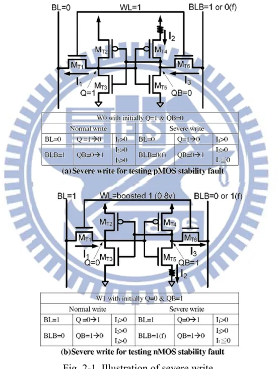
2.4.1 Introduction of Type-B Subthreshold SRAMs
According to the categorization shown in Table 2-I, a Type-B subthreshold SRAM design utilizes a single-ended sense amplifier for read and its read operations share the same path with its write operations. Such a bit-cell structure implies that its write operation is performed through a single bit-line as well, which further increases the difficulty of a write operation. Thus, in order to successfully write data through a single bit-line, Type-B subthreshold SRAM designs heavily rely on the design techniques which can effectively reduce the
hold ability of the cross-coupled inverters during the write operation.
Figure 2-5 shows the first Type-B subthreshold SRAM design [2-12], which can adjust the hold ability of the cross-coupled inverters by controlling the voltage at virtual VDD (VirVDD) and virtual GND (VirGND). During a read operation or the hold mode, VirVDD and VirGND are set to VDD and GND as general SRAMs. During a write operation, VirVDD and VirGND will become an offset lower and an offset higher, respectively, which can break the outside inverter (formed by MB3 and MB4) and allows the voltage at Q to be directly
affected by BL. Also, this design [2-12] utilizes a pMOS pass transistor (MB2) in
addition to a normal nMOS pass transistor (MB1) simultaneously, such that both
1 and 0 can effectively passed through either MB2 or MB1.
Fig. 2-5. First Type-B subthreshold SRAM design [2-12].
Figure 2-6 shows the second Type-B subthreshold SRAM design [2-13], which decreases the hold ability during a write operation by breaking the loop of the cross-coupled inverters through the control signals Wri and WriB (at MB8
and MB7). Once the loop is broken, the value at BL can be easily written into the
bit-cell. After the write operation, the loop of the cross-coupled inverters will be recovered as normal.
Fig. 2-6. Second Type-B subthreshold SRAM design [2-13].
2.4.2 Impact of Open Defects on Type-B Subthreshold SRAMs
Table 2-V lists the minimum detectable resistance and the corresponding faulty behavior of each open defect in Type-B designs. As Table 2-V shows, the open defect at the source/drain of MB4 does not cause a stability fault since the
open defect falls on the path of read-0 and can be easily detected by a read-0 operation (with a 900kΩ minimum detectable resistance). Also, the stability fault at the outside pull-up pMOS MB3 is harder to detect than that at the inside
transistors MB5 and MB6. This is because the outside inverter is either destroyed
or disconnected during a write operation, so that the value at Q is always correct. Even if a defect occurs on the outside pMOS MB3, its weak pull-up ability will
not lead to a wrong value at Q since the value at Q is already set by BL. However, if a defect occurs on the inside inverter, its weak pull-up or pull-down ability may delay the signal at QB and in turn result in a conflict at Q.
Table 2-V also shows that the open defects on the gate and source/drain of MB8 can hardly be detected, implying that the design [2-13] may not really need
a pMOS transistor to pass a value 1 at the outside inverter’s output to Q when the cross-coupled loop is reconnected right after a write operation. In addition, the minimum detectable resistance at each transistor’s gate is still high and hence the corresponding open detect is also hard to detect.
TABLE 2-V
Faulty behavior of open defects on Type-B designs (Fig. 2-5, 2-6). Transistor property Transistor name Transistor terminal Faulty behavior Min detectable resistance Write pass transistor MB1 G W0/R0 fail 2GΩ S/D R0 fail 6.4MΩ MB2 S/D W1 G W1 fail fail 590MΩ 7.6MΩ Outside pull-up pMOS MB3 G W0 fail 4GΩ S/D - ∞ Inside pull-up pMOS MB5 G W0 fail 870MΩ S/D W0 fail 160MΩ Outside pull-down nMOS MB4 G W1 fail 2GΩ S/D R0 fail 900KΩ Inside pull-down nMOS MB6 G W0 fail 970MΩ S/D W1 fail 120MΩ Cross-coupled loop switch MB7 G W1 fail 2GΩ S/D R0 fail 45.8MΩ MB8 G W0 fail 29GΩ S/D - ∞
2.4.3 Effectiveness of Test Methods for Type-B Designs
Table 2-VI reports the minimum detectable resistance achieved by each test method for each stability fault in Type-B designs. Note that the severe write can only be applied to the design utilizing differential write mechanism (with BL and BLB), and hence cannot be applied to Type-B designs, which uses only one bit-line for write. As Table 2-VI shows, only read equivalent stress can detect the most hard-to-detect stability fault (at MB3) in Type-B designs. This is because,
by breaking the hold ability of the cross-coupled inverters, write 1 to Q is easy. As a result, detecting stability fault at MB3 cannot be achieved by using a weak write. We can only rely on read operations to detect it. Also, read equivalent stress can reduce the minimum detectable resistance of the other two stability
faults. In addition, LVW-HVR cannot effectively reduce the minimum detectable resistance at transistors’ gate for Type-B designs as it does for the Type-A designs. Table 2-VII shows the corresponding result at each transistor’s gate. Therefore, read equivalent stress is more preferable than LVW-HVR for Type-B designs overall.
TABLE 2-VI
Effectiveness of test methods for detecting STFs in Type-B designs. Transistor property Transistor name W+R RES LVW-HVR 0.38V-W 0.36V-W Pull-up pMOS MB3 (S/D) ∞ 300KΩ ∞ <0 MB5 (S/D) 160MΩ 160MΩ 150MΩ <0 Pull-down nMOS MB6 (S/D) 120MΩ 62MΩ 43.7MΩ <0 TABLE 2-VII
Effectiveness of test methods for detecting fail-to-write gate open defects in Type-B designs.
Transistor
property Transistor name W+R
LVW-HVR (0.38V-W) Write pass transistor MB1 (G) 2GΩ 2GΩ MB2 (G) 590MΩ 410MΩ Pull-up pMOS MB3 (G) 4GΩ 3GΩ MB5 (G) 870MΩ 790MΩ Outside pull-down nMOS MB4 (G) 2GΩ 430MΩ Inside pull-down nMOS MB6 (G) 970MΩ 410MΩ Cross-coupled loop switch MB7 (G) 2GΩ 3GΩ MB8 (G) 29GΩ 190GΩ
In Table 2-V, open defects on the source/drain of MB1, MB4, and MB7 may
result in a read-0 fail. Since Type-B designs use a single read path and BL is pre-charged to floating 1 for a read operation, a read-1 operation will never fail by an open defect on the bit-cell. In fact, the worst case of performing a read-0 operation occurs when the value of all other bit-cells at the same BL is set to 1, such that the leakage current from MB1 and MB2 can prevent the BL from being
corner and operated at a high temperature. Such a condition can result in a more significant leakage current, even though the pull-down capability of the targeted read path is also increased at a higher temperature (will discuss more in Section 2.8).
In the following experiment, we attempt to observe the impact of setting the data of all other bit-cells at the same BL to the same value (0) or the opposite value (1) to the accessed bitcell when performing a read-0 operation in Type-B designs. Table 2-VIII lists the minimum detectable resistance of the three read-0-fail open defects with both background settings. The simulation is conducted based on the FF corner at 75˚C. As the result shows, with the same data background, a large open defect may not be even detectable since the leakage at the same BL can help to pull down the data. With the opposite background, the minimum detectable resistance can be significantly reduced. Note that we have tried a similar experiment to Type-A designs but its difference of using different backgrounds is limited.
TABLE 2-VIII
Impact of using different backgrounds when testing fail-to-read open defects in Type-B designs.
Transistor name Same background Opposite background MB1 (S/D) ∞ 8.1MΩ
MB4 (S/D) ∞ 90KΩ
MB7 (S/D) 150MΩ 20.4MΩ
To apply this all-1 background for a read-0 operation at each bit-cell, the march sequence in use needs to include the march element (w0, r0, w1). This march element can generate a read 0 out of an all-1 BL background and then recover the target bit-cell to 1, such that the background can remain all 1 when moving to the next address. Note that the march element (w0, r0, w1) is not included in a conventional SRAM march sequence, such as March C-.
2.5 Analysis of Open Defects in Type-C Subthreshold SRAMs
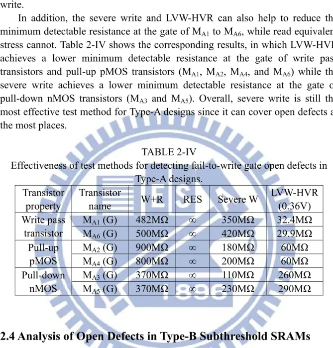
2.5.1 Introduction of Type-C Subthreshold SRAMs
SRAM design utilizes a differential sense amplifier for read and its read path is different from its write path. It means that each of Q and QB needs to be read out through a different extra read path to BL or BLB instead of through the pull-up or pull-down paths of the cross-coupled inverters. Once the read paths are independent from the cross-coupled inverter, the read static noise margin can be protected. Also, Type-C subthreshold SRAM designs utilize a virtual GND to destroy the original stored data and improve its write ability.
Figure 2-7 shows the first Type-C subthreshold SRAM design [2-14], which embeds a 6T-SRAM design (with MC2, MC4, MC5, MC6, MC7, and MC8) in the
center and one extra read path on a side to read out the value of Q (with MC1 and
MC3) or QB (with MC9 and MC10). Also, two word-lines (WL1 and WL2) are
used in this design. During a read operation, WL1 is set to 0 and WL2 is set to 1. Then the pre-charged BL will be pulled down by MC3 if Q = 1 and will remain
floating 1 if Q = 0, meaning that the value read out from BL (or BLB) is different from the value at Q (or QB). During a write operation, both WL1 and WL2 are set to 1 and virtual GND is pulled up to VDD, which changes the original stored value at Q and QB to a voltage around 0.5 VDD and provides a weaker initial value at the cross-coupled inverters for write. After the write operation, the virtual GND will be pulled down to GND, which separates the voltages at Q and QB further apart. During the hold mode, both WL1 and WL2 are set to 0.
Fig. 2-7. First Type-C subthreshold SRAM design [2-14].
Figure 2-8 shows the second Type-C subthreshold SRAM design [2-15], which further improves the first Type-C design [2-14] with the following modification. In [2-15], its BL is connected to the output of the inverter formed
by MC6 and MC7 (through MC1 and MC2) instead of that by MC4 and MC5.
Similarly, its BLB is connected to the output of the inverter formed by MC4 and
MC5 (through MC8 and MC10). As a result, the value read out at BL will be the
same as the value at Q. Also, during its hold mode, WL2 is set to 0 but WL1 is set to 1. Under this setting of word-lines, MC3 or MC9 can help to pull down QB
or Q during the hold mode, which can further increase its hold ability. In addition, because the value at Q equals to the value at BL during a read operation, the leakage of MC2 in [2-15] can be significantly reduced when
compared to [2-14]. Similar situation applies to the leakage of MC8 during a read operation. Since [2-15] is a more refined version of [2-14], we will only consider the case of [2-15] in our later discussion regarding Type-C subthreshold SRAM designs.
Fig. 2-8. Second Type-C subthreshold SRAM design [2-15].
2.5.2 Impact of Open Defects on Type-C Subthreshold SRAMs
Table 2-IX lists the minimum detectable resistance and the corresponding faulty behavior of each open defect in Type-C designs. As Table 2-IX shows, the stability faults on the nMOS transistors MC5 and MC7 cannot be detected at all.
However, the stability faults on the pMOS transistors MC4 and MC6 are relatively
easy to detect (with 11MΩ minimum detectable resistance), even compared to other stability faults in Type-A and Type-B designs. This is because the write mechanism in Type-C design relies on MC4 (or MC6) to strongly hold the value 1
at QB (or Q) at the end of a write-0 operation, while VirGND just turns from VDD to GND. Thus, a small open defect on the source/drain of MC4 or MC6 may
fail the write operation. In addition, the open defect at a transistor’s gate is also relatively easier to detect when compared to that in Type-A and Type-B designs.
TABLE 2-IX
Faulty behavior of open defects on Type-C designs (Fig. 2-7, 2-8). Transistor property Transistor name Transistor terminal Faulty behavior Min detectable resistance Write only
pass transistor MC2 & MC8
G W1 fail 58MΩ S/D W1 fail 16MΩ Write/read
pass transistor MC1 & MC10
G R1 fail 39MΩ S/D R1 fail 2MΩ Pull-up pMOS MC4 & MC6 G W1 fail 64MΩ S/D W0 fail 11MΩ Pull-down nMOS MC5 & MC7 G W1 fail 410MΩ S/D - ∞ Read-path pull-down MC3 & MC9 G W1 fail 170MΩ S/D R1 fail 3MΩ
2.5.3 Effectiveness of Test Methods for Type-C Designs
Table 2-X reports the minimum detectable resistance achieved by each test method for each stability fault in Type-C designs. As the result shows, only LVW-HVR can detect the stability faults on nMOS transistors MC5 and MC7
while both RES and severe write cannot. However, the write voltage for LVWHVR need to be carefully assigned such that the nMOS stability faults can be detected and the fault-free design can still correctly function.
TABLE 2-X
Effectiveness of test methods for detecting STFs in Type-C designs. Transistor
property
Transistor
name W+R RES Severe write
LVW-HVR (0.26v) Pull-up pMOS MC4 (S/D) 11MΩ 17MΩ 6MΩ 930KΩ MC6 (S/D) Pull-down nMOS MC5 (S/D) ∞ ∞ ∞ 16MΩ MC7 (S/D)
Table 2-XI shows the corresponding result of applying different write voltages to LVW-HVR. As the result shows, LVW-HVR cannot detect nMOS stability faults until the write voltage is reduced to 0.26V. However, if we further lower the write voltage to 0.24V, the minimum detectable resistance of pMOS and nMOS stability faults will be reduced to 2KΩ and 45KΩ. Such a low minimum detectable resistance kills almost all design margin for tolerating small detects during the test mode and in turn may result in an over-testing. Therefore, setting a proper write voltage is critical when applying LVW-HVR.
TABLE 2-XI
Impact of using different write voltages during LVW-HVR for Type-C designs. Transistor
property
Transistor name
LVW-HVR with different write voltage (0.30v) (0.28v) (0.26v) (0.24v) Pull-up pMOS MC4 (S/D) 4MΩ 3MΩ 930KΩ 2KΩ MC6 (S/D) Pull-down nMOS MC5 (S/D) ∞ ∞ 16MΩ 45KΩ MC7 (S/D)
Similar to Table 2-VIII, Table 2-XII reports the minimum detectable resistance obtained by applying the same background and the opposite background for all read-fail open defects in Type-C designs. The simulation is also conducted based on the FF corner at 75˚C. As the result shows, the opposite data background can effectively help to detect those read-fail open defects (with an acceptable minimum detectable resistance) while the same data background may fail to detect a large open defect, which again shows the effectiveness of setting an opposite background for detecting a read-fail open defect.
TABLE 2-XII
Impact of using different backgrounds when testing fail-to-read open defects in Type-C designs.
Transistor name Same background Opposite background MC1 (G) ∞ 310MΩ
MC1 (S/D) 78MΩ 7MΩ
2.6 Address Decoder Faults in Subthreshold SRAMS
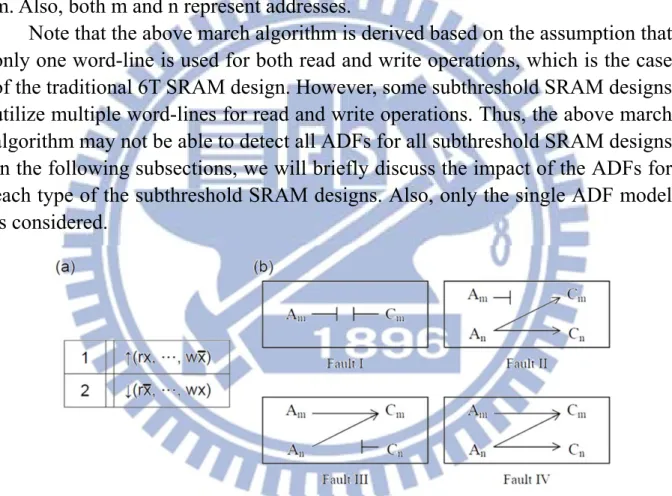
Address decoder faults (ADFs) in memories have been studied in the past [2-22] [2-23] [2-24], and it is proven in [2-24] that all the gross ADFs (not including the faults with sequential behavior and the small timing defect in the address decoder) can be detected by a march algorithm as long as the two march elements in Figure 2-9(a) are included. Figure 2-9(b) shows the four gross ADFs defined in [2-24]. In Figure 2-9(b), Am represents the word-line signal of the
address m, and Cm represents the physical memory cell indexed by the address
m. Also, both m and n represent addresses.
Note that the above march algorithm is derived based on the assumption that only one word-line is used for both read and write operations, which is the case of the traditional 6T SRAM design. However, some subthreshold SRAM designs utilize multiple word-lines for read and write operations. Thus, the above march algorithm may not be able to detect all ADFs for all subthreshold SRAM designs. In the following subsections, we will briefly discuss the impact of the ADFs for each type of the subthreshold SRAM designs. Also, only the single ADF model is considered.
Fig. 2-9. (a) Conventional march sequence for detecting ADFs; (b) Types of address decoder faults.
2.6.1 Type-A Subthreshold SRAM
Type-A subthreshold SRAM designs use separate read wordline and write word-line (denoted as RWL and WWL in Figure 2-2 to 2-4) for read operations and write operations, respectively. Each ADF shown in Figure 2-9 may occur on
each of these two wordlines, and hence we need to consider total 8 cases of ADFs (4 types of ADFs on two word-lines). In the following paragraphs, the 8 cases of ADFs would be discussed.
1) Fault-I: When Fault-I exists and occurs on the WWL, the cell Cm (refer
Figure 2-9(b)) would be unaccessible when it should be written, but accessible for reading. The sense amplifier (SA), when reading Cm, would thus always output the same value as the pre-stored data in Cm. The SAF-like behavior can
be easily tested by the march in Figure 2-9(a). In the other case of Fault-I occurring on the RWL, since the RWL of Cm will never be triggered, the voltage
on RBL (refer Figure 2-2 to 2-4) when reading Cm will always keep high
regardless of the value in Cm. The faulty behavior is just like SA1 and can also
be tested by the Figure 2-9(a) march.
2) Fault-II: When Fault-II occurs on the WWL, Cm could not be written by
system operation ”Write Cm” but by the “Write Cn”. The faulty behavior can be
tested by Figure 2-9(a) march. It’s because, in either ↑ rx, … , w ̅ or ↓ r ̅, … , wx where Cn is earlier accessed than Cm, the ”Read Cm” will output
the inverse value since the previous ”Write Cn” operation changes the value
stored in Cm. In the other case of occurring on the RWL, Cm is unaccessible for
read operation and thus the SA output of operation ”Read Cm” will always keep
high as Fault-I on RWL. The SA1-like behavior is testable by the Figure 2-9(a) march.
3) Fault-III: In the faulty behavior of Fault-III occurring on WWL, Cm
would be written by operation ”Write Cn” just like Fault-II on WWL. Thus in
either ↑ rx, … , w ̅ or ↓ r ̅, … , wx where Cn is earlier accessed than Cm, the
SA output of ”Read Cm” will be the inverse value written by operation ”Write
Cn”. Figure 2-9(a) march is still useful for Fault-III on WWL. For Fault-III on
RWL, Figure 2-9(a) is still useful but uses the different test element from on-WWL case. In the march element in which Cm is earlier accessed than Cn,
the ”Read Cn” will read the value in Cm, which is changed by previous
operation ”Write Cm”, rather than unchanged value in Cn.
4) Fault-IV: Fault-IV on WWL is just like Fault-II/III on WWL which can be tested by the march element in which Cn is earlier accessed than Cm. The
detail can be referred in previous paragraph. For Fault-IV occurring on RWL, its write operation works correctly but when reading cell n, both Cm and Cn will be
read out at the same time. Assuming that m > n in the ADF Fault-IV (i.e., ↑ will visit n earlier than m), the march element ↑ rx, … , w ̅ march element cannot detect the ADF Fault-IV because both Cn and Cm store the same value x when
necessarily detect the ADF Fault-IV. For example, even though the march element ↓ r0, … , w1 can create the situation that Cn stores 0 and Cm stores 1
when reading Cn, the RBL remains the good value 0 because the read bit-line
will not be pulled up by the value 1 of cell m for designs [2-10] and [2-11]. The read-1 mechanism in [2-10] and [2-11] is to turn off the pull-down path at the read bit-line and leave the read bit-line floating 1. Thus, only the march element ↓ r1, … , w0 can detect the ADF Fault-IV in this case. Note that the above discussion is based on the assumption that m > n in the ADF Fault-IV. To cover the case that that m < n, another march element ↑ r1, … , w0 is also required.
5) Short Summary: After the analysis, most cases of ADFs can be detected by the march algorithm shown in Figure 2-9(a). However, the case of Fault-IV occurring on the RWL needs both ↓ r1, … , w0 and ↑ r1, … , w0 Therefore, a march algorithm which can cover four ADFs for Type-A SRAM designs needs to include three march elements. The two possible combinations of the three march elements are (1) ↓ r1, … , w0 , ↑ r1, … , w0 , and ↓ r0, … , w1 , and (2) ↓ r1, … , w0 , ↑ r1, … , w0 , and ↑ r0, … , w1 .
2.6.2 Type-B Subthreshold SRAM
Type-B subthreshold SRAM designs utilize WL and WL to access a bit-cell for both read and write operations. In general, these two signals (WL and ) come from the same address decoder but with the difference of an inverter. Thus, once an ADF falls in the address decoder, the signal at both WL and will be affected. As a result, the impact of an ADF fault in Type-B Subthreshold SRAM designs is exactly the same as that in a 6T SRAM design, and hence the march algorithm shown in Figure 2-9(a) is sufficient to detect all the ADFs for Type-B Subthreshold SRAM designs.
2.6.3 Type-C Subthreshold SRAM
The analysis of ADFs in Type-C subthreshold SRAM design [2-15] is more complicated than that in Type-A or Type-B designs since the Type-C design uses the combination of the values at WL1 and WL2 to determine the operation mode of a cell. Table 2-XIII shows the value of WL1 and WL2 at its hold, read, and write mode, respectively.
TABLE 2-XIII
Setting of WL1 and WL2 for Type-C design Operation WL1 WL2
Hold 1 0 Read 0 1 Write 1 1
A full analysis of ADFs in the Type-C design should include the impact of each ADF on each word-line (total 4 ADFs for 2 word-lines). For each ADF on each word-line, we need to enumerate the value at each word-line caused by the ADF based on different operation modes of the two faulty cells, which includes four effective combinations: Cm/Cn= (1) Read/Hold, (2) Write/Hold, (3)
Hold/Read, and (4) Hold/Write. Note that we eliminate the cases of simultaneous Read and/or Write (i.e. Read/Read, Read/Write, Write/Read, and Write/Write) since the subthreshold SRAM is a single-port SRAM.
Table 2-XIV lists the complete analysis results of WL1 and WL2 values of the Type-C design [2-15] under the four Cm/Cn operations when each of the
ADFs in Figure 2-9(b) occurs on WL1 and WL2 separately. According to the setting in Table 2-XIII, the values of WL1 and WL2 will lead to the corresponding behavior listed in the ”Behavior” columns of Table 2-XIV. If the corresponding behavior is different from the supposed one, we highlight the faulty behavior with a gray background in Table 2-XIV. Note that we view the combination WL1=WL2=0 as a Hold operation since this configuration also enables the Type-C design [2-15] to hold the data but just without the extra assistance of MC3 and MC9.
The faulty behaviors in Table 2-XIV are categorized into four groups (FB1-USR, FB2-UA, FB3-AR, and FB4-AW). In the paragraphs below, we will detail how each faulty behavior performs and give a short summary for testing ADFs in the Type-C design at the end.
1) FB1-USR (UnSafe Read) : The faulty behavior FB1-USR means that a cell is supposed to be read out, but its value may be attacked during the read operation. As shown in Table 2-XIII, only WL2 should be turned on during a read operation such that the turned off WL1 can protect the cross-coupled inverters from BL/BLB’s direct accessing (as illustrated in Figure 2-8). The cell with the faulty behavior FB1-USR would have both its word-lines turned on during a read operation, and thus the stored data (Q and QB) would be affected by the pre-charged BL/BLB just as the typical 6T SRAM would. In other words, the designed extra-read path in the Typc-C subthreshold SRAM is disabled and
TABLE 2-XIV
![Fig. 4-16 GOS defect with nine different locations…………………………70 Fig. 4-17 Design-for-test (DfT) of weak write test mode [4-45]……………74 Fig](https://thumb-ap.123doks.com/thumbv2/9libinfo/8140570.166658/16.892.112.816.124.991/fig-gos-defect-different-locations-fig-design-write.webp)
![Figure 2-5 shows the first Type-B subthreshold SRAM design [2-12], which can adjust the hold ability of the cross-coupled inverters by controlling the voltage at virtual VDD (VirVDD) and virtual GND (VirGND)](https://thumb-ap.123doks.com/thumbv2/9libinfo/8140570.166658/33.892.166.787.369.791/figure-subthreshold-inverters-controlling-virtual-virvdd-virtual-virgnd.webp)
![Figure 2-7 shows the first Type-C subthreshold SRAM design [2-14], which embeds a 6T-SRAM design (with M C2 , M C4 , M C5 , M C6 , M C7 , and M C8 ) in the center and one extra read path on a side to read out the value of Q (with M C1 and M C3 ) or QB](https://thumb-ap.123doks.com/thumbv2/9libinfo/8140570.166658/38.892.130.812.226.998/figure-subthreshold-sram-design-embeds-sram-design-center.webp)