以Balsa實作之非同步JPEG解碼器
65
0
0
全文
(2) CONTENTS An Asynchronous JPEG Decoder Designed with Balsa ............................................ i LIST OF TABLES............................................................................................................ iv LIST OF FIGURES ........................................................................................................... v ACKNOWLEDGMENT ................................................................................................ viii ABSTRACT ..................................................................................................................... ix 1. Introduction.................................................................................................................. 1 1.1 Less is More ....................................................................................................... 1 1.2 Not at the same time ........................................................................................... 1 1.3 No! It’s not an e-mail client ............................................................................... 2 1.4 Lose to gain ........................................................................................................ 6 2. Related Work ............................................................................................................... 7 2.1 ISO 10918-1 ....................................................................................................... 7 2.1.1 Entropy Coding ...................................................................................... 7 2.1.2 Quantization ........................................................................................... 8 2.1.3 Discrete Cosine Transform .................................................................... 9 2.2 Classification of Asynchronous Circuits.......................................................... 12 2.3 Balsa Back-End ................................................................................................ 13 2.3.1 Basic Elements ..................................................................................... 13 2.3.2 Handshake Components ....................................................................... 18 2.4 Concluding Remarks ........................................................................................ 20 3. Designing the JPAD .................................................................................................. 22 3.1 JPAD overview ................................................................................................ 22 3.2 Dissecting JPAD .............................................................................................. 23 3.2.1 Bit Supply Unit .................................................................................... 23 3.2.2 Huffman Decoder ................................................................................. 24 3.2.3 Extender ............................................................................................... 26 ii.
(3) 3.2.4 Dequantizer .......................................................................................... 28 3.2.5 Control Unit ......................................................................................... 28 3.3 Make the Common Case Fast .......................................................................... 31 4. Implementation and Verification ............................................................................... 34 4.1 The VLSI and FPGA design flow for asynchronous circuit using Balsa ........ 34 4.2 Implementation Issues...................................................................................... 36 4.3 Verification ...................................................................................................... 38 5. Simulation Result....................................................................................................... 41 5.1 Accuracy Analysis ........................................................................................... 41 5.1.1 PSNR. 41 . 5.1.2 Samples of PSNR ................................................................................. 41 5.1.3 PSNR in numbers ................................................................................. 49 5.2 Area Cost.......................................................................................................... 51 6. Conclusion, Confession and Future Work ................................................................. 55 References........................................................................................................................ 56 . iii.
(4) LIST OF TABLES Table 1 : Count of Code Lengths for AC Component 1 ................................. 24 Table 2 : Huffman Decoding Data................................................................... 25 Table 3 : PSNR of 6 different pictures in YUV color space ........................... 50 Table 4 : A List of Total Equivalent Gate Counts ........................................... 51 Table 5 : A List of Total Cell Areas ................................................................ 52 . iv.
(5) LIST OF FIGURES Figure 1: The 4-Phase Bundled Data Interface Protocol ................................... 2 Figure 2: Handshake Circuit for a single-place buffer .................................... 3 Figure 3: code for a single-place buffer ............................................................. 4 Figure 4: The Complete Balsa Design Flow...................................................... 5 Figure 5 : DCT-based decoder simplified diagram ........................................... 7 Figure 6 : Zig-Zag Sequence ............................................................................. 8 Figure 7 : Resulting Picture from Quantization ................................................. 9 Figure 8 : An Example of Quantization Table................................................... 9 Figure 9 : DCT compared with DFT of an input signal .................................. 10 Figure 10 : 64 squares of different frequencies ............................................... 11 Figure 11 : A Circuit Segment with Gate and Wire Delays ............................ 12 Figure 12 : The Muller C-Element as (i)Gate-Level Implementation, (ii)Transistor-Level Implementation, (iii)Logic Symbol, (iv) Truth Table ................................................................................................................. 13 Figure 13 : The NC2P-element as (i) Logic Symbol (ii) Truth Table (iii) GateLevel (iv) Transistor-Level Implementation ........................................... 15 Figure 14 : The S-element as (i) Functional Block (ii) Gate-Level Implementation (iii) Handshaking Protocol ............................................ 16 Figure 15 : The Multiplexer as (i)Logic Symbol (ii) Truth Table (iii) GateLevel Implementation .............................................................................. 17 Figure 16 : The De-Multiplexer as (i) Functional Block (ii) Truth Table (iii) Gate-Level Implementation ..................................................................... 17 Figure 17 : The Fetch Component as (i) Symbol (ii) Gate-Level Implementation ........................................................................................ 18 Figure 18 : The Sequence Component as (i) Symbol (ii) Gate-Level Implementation ........................................................................................ 19 Figure 19 : The Concurrent Component as (i) Symbol (ii) Gate-Level Implementation ........................................................................................ 19 Figure 20 : The Variable Component as (i) Handshake Component (ii) GateLevel Implementation .............................................................................. 20 v.
(6) Figure 21 : The Architecture of JPAD ............................................................. 22 Figure 22 : Partial Code of BSU ...................................................................... 23 Figure 23 : Partial Code of BSU – Continued ................................................. 24 Figure 24 : Code Snippet of Huffman Decoder ............................................... 26 Figure 25 : Magnitude Codes and Ranges ....................................................... 27 Figure 26 : Partial Code of Extender ............................................................... 27 Figure 27 : Structure of a JPEG File............................................................... 28 Figure 28 : A Code Snippet searching for X”FFDB” from Control Unit ........ 29 Figure 29 : A Code Snippet writing 64 values to quantization table ............... 29 Figure 30 : A Code Snippet performing Huffman DC decoding..................... 30 Figure 31 : Indexable Zig-Zag Sequence......................................................... 31 Figure 32 : The 3 Pipeline Stages of IDCT ..................................................... 32 Figure 33 : 3 Stages connected in parallel ....................................................... 33 Figure 34 : Data flow diagram of IDCT .......................................................... 33 Figure 35 : The FPGA design flow of Balsa ................................................... 35 Figure 36 : The VLSI Design Flow of Balsa ................................................... 36 Figure 37 : JPAD Behavior Simulation Environment ..................................... 38 Figure 38 : Balsa Description for Memory Model .......................................... 38 Figure 39 : User Interface of Hex2ASCII........................................................ 39 Figure 40 : User Interface of ASCII2BMP ...................................................... 40 Figure 41 : Mona Lisa...................................................................................... 42 Figure 42 : Y Component of Mona Lisa.......................................................... 43 Figure 43 : U Component of Mona Lisa.......................................................... 44 Figure 44 : V Component of Mona Lisa.......................................................... 45 Figure 45 : Spiderman3® ................................................................................. 46 Figure 46 : Y Component of Spiderman3®...................................................... 47 Figure 47 : U Component of Spiderman3®...................................................... 48 Figure 48 : V Component of Spiderman3®...................................................... 49 Figure 49 : PSNR Displayed in Bars ............................................................... 50 Figure 50 : Official Sample ............................................................................. 51 Figure 51 : Gate Counts Displayed in a Pie ..................................................... 52 vi.
(7) Figure 52 : Cell Areas Displayed in a Pie........................................................ 53 Figure 53 : Cell Areas from a 16-bit MUL scheme ......................................... 54 . vii.
(8) ACKNOWLEDGMENT First and foremost, I would like to thank everyone who made it possible for the thesis to come out. Without their support (and urge), this piece of work would not have been achievable. I want to thank Department of Computer Science for providing me with invaluable resources, thus enabling me to study and research in the first place. I am forever in debt of gratitude to my supervisor, Prof. Chen, for his instruction and enlightenment on both my academic and spiritual paths. I deeply appreciate the laboratory members, many other friends and peers for their good company through all these 3 years to prevent me from being too depressed. Especially, I will give special thanks to my mother, who understood my dilemma and inner struggles (and perhaps laziness) which caused me not to graduate in time.. viii.
(9) ABSTRACT Asynchronous circuits have been more and more popular these days, since there is an increasingly dire need for more efficient use of energy, resulted from not only limited battery life but also concerns for global warming. However, asynchronous circuits have a nature that renders them difficult to design and verify. With the invention of Balsa programming environment, people can forge their “asynchronous” ideas into reality more easily by the help of its synthesis and simulation tools. A JPEG decoder was chosen as the object of implementation because it was tested by time, as well as sophisticated enough to show the viability of this design flow or methodology. A pipeline structure was also added to hasten computation of the most time-consuming part, the IDCT. Furthermore, the 4-phase bundled data approach was taken in this example to facilitate development and avoid excess area cost generated otherwise by a dual-rail version.. ix.
(10) 1. Introduction 1.1 Less is More Not until recently did so many scientists devote themselves to the research of more power saving methods. Once people have calculation speeds enough to meet the requirements of most applications, they move on to make those devices more efficient─ that is─ operating on less power while not affecting their functionality. This can be seen especially from the ever growing number of hand-held or mobile devices such as notebook computers, PDAs, cell-phones, music/video players……etc. All of these necessitate longer time of use while powered by fast-draining batteries. Unfortunately, the technologies of batteries aren’t evolving at the same pace as those of semiconductors, hence compelling us not to rely on the battery capacity but on our own change of ideas. Some techniques like clock gating found in low-power synchronous circuits, cache resizing or word-line gating of caches in microprocessors, or fine-grain dynamic leakage reduction to reduce intrinsic static leakage current from CMOS. Nonetheless, they are highly dependent on the type of implementation, and they may pose certain headaches to the developers. On the other hand, asynchronous circuits have a low-power nature which derives from their total lack of global clocks. Furthermore, they are applicable with any transistor-based technologies.. 1.2 Not at the same time What exactly is an asynchronous circuit? You might ask. Here let me take something of my favorite for example. Imagine that several cars are running on the road and suddenly the light turns red. The first car stops, then second, third …… until the last car in line does. After a while the light changes its color, and the cars accelerate in the same order from the first one to the last one. Every single car must react to the action its frontal car takes. If you are comparing asynchronous circuit to road traffic, then an asynchronous component is just like a car. It means that no component should make a request for input/output data unless the next component is ready, and certainly it must signal or 1 .
(11) inform the last component it connects to upon completion. Well if you are familiar with internet and TCP/IP you must have heard of 3-Way handshake, but we don’t need 3-way in an electronic circuit since the correctness of data is guaranteed, if not 100%. Shown below is one of such handshake protocols.. Figure 1: The 4-Phase Bundled Data Interface Protocol As you probably guessed, an asynchronous component is active only if spatiotemporally required, therefore consuming energy in the right place at the right time. This most noticeable feature is what its synchronous counterpart cannot simulate, with clocks ticking everywhere. Everything has a price though. It takes a certain amount of time before we can step on the pedals because of our limited reflexes. Same goes for handshake protocols, the extra circuitry added for coordinating asynchronous signals and data also puts a great burden on the area cost and operating speed. That’s why few practitioners of asynchronous design compare their results with synchronous ones in respect to performance. With these drawbacks in mind, one shouldn’t be too particular about speed or cost when he decides to tread this path. Ailed by the difficulties such as possibility of data hazards, lack of commercial tools, let alone insufficient experience, we shouldn’t further trouble ourselves by doing gate-level design. Therefore, to aid our work, we adopted Balsa, a high-level asynchronous-specific language, which was developed at Manchester University, in the design process.. 1.3 No! It’s not an e-mail client According to the authors, “Balsa is the name of both the framework for synthesizing asynchronous hardware systems and the language for describing such. 2.
(12) systems”. Interestingly, if you look up the word in the dictionary, it says a tropical American tree or a life raft, since they are UK but US, it must be referring to the latter. I’m quite satisfied with the answer I found since at least it saves you a lot of time/life. What it does is simply translate your syntax into communicating handshake components which closely follow Tangram(1). They call their own interpretation of Tangram as Breeze(since it must be hot rafting under the blazing sun). To see how it looks, here is an example:. Figure 2: Handshake Circuit for a single-place buffer A filled circle represents an active port, sending requests to the unfilled circle, which is a passive port. Sequencer “;” ensures that activities on the left side finish before those on the right side. Fetch component “→” causes data to be moved to the storage element of Variable x. When these operations are complete, the Sequencer completes its handshake with the repeater which initiates the cycle again. It is relatively simple, composed of only a few lines.. 3.
(13) Figure 3: code for a single-place buffer We will use loop structures very extensively in the making. Another feature worth noting also is its ability to generate a netlist from a breeze description. The netlist could then be manually tweaked to be uploaded onto FPGA, or be ready for a layout. Now is a good time to introduce its full design flow to the curious eyes.. 4.
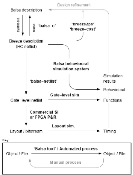
(14) Figure 4: The Complete Balsa Design Flow As the self-explanatory figure reveals, a Balsa description of a circuit is compiled using balsa-c to an intermediate breeze description. Most of the Balsa tools are in charge of manipulating the breeze handshake intermediate files. Behavioral simulation is provided by breeze-sim. This simulator allows source level debugging, visualization of the channel activity at the handshake circuit level as well as producing conventional waveform traces that can be viewed using the waveform viewer gtkwave. balsa-netlist produces a netlist appropriate for the target technology or CAD framework from a Breeze description. Now that we are confident of its great potential, we should put it into good use by doing something huge, yet not exhausting our system resources. After some surveying, 5.
(15) pondering and dithering, I thought the enduring image format JPEG would be best to assume the role. Moreover, a standalone decoder would be more than enough to assume it, for the procedures concerned are quite similar between a decoder and an encoder.. 1.4 Lose to gain There are quite a few image compression formats, of which the most well-known ones are GIF, PNG and JPEG. GIF adopts the LZW lossless data compression technique to reduce the file size without degrading the visual quality, however, its 256-color limitation makes it virtually useless dealing with photos. Depending on usage, PNG can be lossless or lossy, and is quite efficient tackling large blocks of the same colors. Among all of the formats, JPEG is the most commonly used standard method of compression for photographic images. The compression method is usually lossy compression, meaning that some visual quality is lost in the process, although there are variations on the standard baseline JPEG which are lossless. There is even a progressive format, in which data is compressed in multiple passes of progressively higher detail. This allows for a quick preview before all the data has been downloaded. However, progressive JPEGs are not as widely supported. Based on the aforementioned circumstances, I decided that a baseline JPEG decoder would be best for implementation this time to take advantage of its popularity and versatility.. 6.
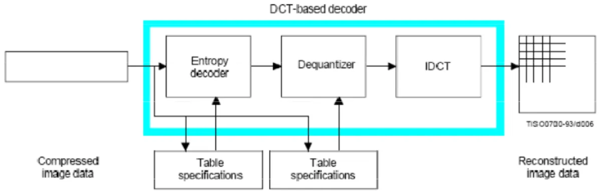
(16) 2. Related Work This chapter circles around three axes. First we will start out by sharing a brief view at the JPEG specifications and its mechanism. Then we will describe different categories of asynchronous circuits regarding delay assumptions. Finally we will introduce several frequently encountered basic cells generated automatically by Balsa synthesis tool.. 2.1 ISO 10918-1 The name JPEG stands for Joint Photographic Experts Group, the name of the committee who created the standard. The group was organized in 1986, issuing a standard in 1992 which was approved in 1994 as ISO 10918-1(2). Its decoding process can be easily visualized with the help of the following diagram.. Figure 5 : DCT-based decoder simplified diagram As we can see, a decoding process converts compressed image data to reconstructed image data through three main stages, entropy (Huffman) decoder, dequantizer and IDCT, with the first two having their own tables. 2.1.1 Entropy Coding In information theory an entropy coding is a lossless data compression scheme that assigns codes to symbols so as to match code lengths with the probabilities of the symbols. In JPEG, it is useful to consider entropy coding as a 2-step process. The first 7.
(17) step converts the zig-zag sequence of quantized coefficients into an intermediate sequence of symbols. The second step involves converting the symbols to a data stream in which external boundaries of the symbols totally disappear. Figure 6 shows the zigzag sequence where the first block represents the DC component and the rest AC components.. Figure 6 : Zig-Zag Sequence The DC and AC symbols take the forms (SIZE)(AMPLITUDE) or (RUNLENGTH,SIZE) (AMPLITUDE) respectively(3). To be clear, Runlength is the number of zeros encountered along the zig-zag path before a non-zero number. JPEG adopts the somewhat weird scheme because zeros are frequent and certain sizes of numbers are more frequent than the others. We’ll go in detail about this later. 2.1.2 Quantization The human eye is good at seeing small differences in brightness over a relatively large area, but not so good at distinguishing the exact strength of a high frequency brightness variation. This fact allows one to deceive the eye by greatly reducing the amount of information in the high frequency components only. This is done by simply dividing each component in the frequency domain by a constant for that component, and then rounding to the nearest integer. This is what makes JPEG lossy in the whole process. Figure 7 demonstrates the result from such operation.. 8.
(18) Figure 7 : Resulting Picture from Quantization It is usually the case that many of the higher frequency components are rounded to zero, and many of the rest become small positive or negative numbers, which take far fewer bits to store. There can be multiple quantization tables for an image file, and a common quantization matrix may just look like Figure 8.. Figure 8 : An Example of Quantization Table The first number 16 in the upper left corner stands for dividing by 16 and rounding it. Magnitude grows diagonally to the lower right as frequency increases. It’s advised to load the tables from the file since they differ from one image to another. 2.1.3 Discrete Cosine Transform A discrete cosine transform (DCT) is a Fourier-related transform similar to the discrete Fourier transform (DFT), but using only real numbers. DCTs can be thought of as DFTs with double length, operating on real data with even symmetry (since the 9.
(19) Fouurier transfo form of a reeal and evenn function is real and eeven). It is superfluouss to apply D DFT on pictures for thhey are not in time buut in spatiall domain. In n JPEG thee input or ouutput data are a shifted by b half a sample (128 for f an 8-bitt sample), before b beingg processed by DCT or IDCT.. Figurre 9 : DCT compared with DFT of o an inputt signal Forrmally, the DCT is a linear, inverrtible functiion F:. N. →. N. (wheree R denotess. the set of real numbeers), or equuivalently an a N by N square mattrix. The reeal numberss x , …, xN. are trannsformed innto the N rreal numberrs X , …, X N. according to thee. formula: X. 2c k N. N. x cos. 2j. 1 kπ 2 2N k = 0, 1, …, N – 1. and the invverse transfo form is N. x. c k X cos. 2j. 1 kπ 2N N. j = 0, 1, …, N – 1 where c(kk) =. √. = 1. foor k = 0 foor k = 1, 2, …, N – 1. 1 10.
(20) The transform m possesses a high enerrgy compacction properrty which is superior to o any known n transform m with a faast computaational algo orithm. Its llinear property furtherr enables dirrect expansiion into a tw wo-dimensional DCT. A 2D DCT is defined as: a X. ,. 2 c u c v N. N. N. x. cos. ,. 2i. 1 uπ 2j 1 vπ cos 2N 2 2N. u、v = 0, 1, …, N-1 D IDCT as: and the 2D x,. 2 N. N. N. c u c v X. ,. cos. 2i. 1 uπ 2 2j 1 vπ cos 2N 2N N. i、j = 0, 1, …, N-1 N where u), c(v) = 1⁄√2 for u,v u =0 c(u c(u u), c(v) = 1 otherwisee.. Figure 10 : 64 6 squares of differen nt frequencies The 2D DCT transforms 64 pixels of o a block to a linear combinatio on of the 64 4 squares sh hown above in Figure 10. 1 It may seeem a hugee number off multiplicattions at firstt glance. Foortunately, after a some evaluation we realize that it can be decomp posed into 8 rows of DC CT followed by 8 colu umns of DCT T, or vice versa. v Theree are severall algorithmss to acceleraate DCT wh hich will be discussed later. 1 11.
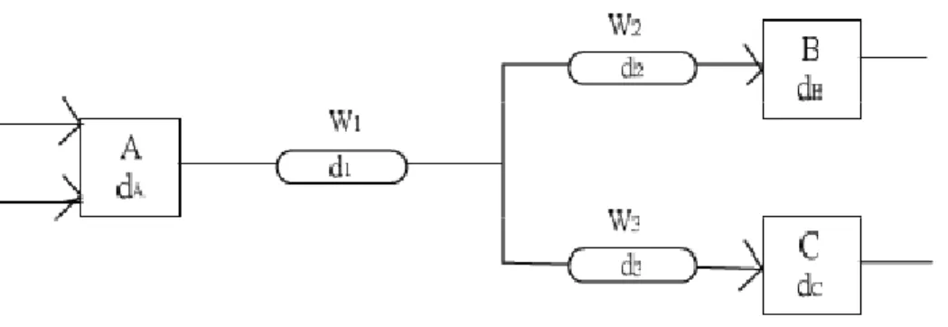
(21) 2.2 Classification of Asynchronous Circuits. Figure 11 : A Circuit Segment with Gate and Wire Delays At the gate level, asynchronous circuits can be classified as being delayinsensitive, quasi-delay-insensitive, speed-independent, or self-timed depending on the delay assumptions that are made(4). Figure 11 serves to illustrate the following discussion. In this figure there are three gates (A, B, C) and three wires (W , W ,W ). dA , dB , and dC represent the gate delays for A, B, and C, while d , d , and d represent the wire delays for W , W , and W respectively. (a) Delay-Insensitive (DI): A circuit that operates correctly with positive, bounded but unknown delays in wires and gates. Recalling figure11, this is equivalent to arbitrary dA , dB , dC , d , d , and d . Unfortunately, assuming ideal zero-delay wires is not very realistic in today’s semiconductor processes. (b) Quasi-Delay-Insensitive (QDI): a QDI circuit is DI with the exception of some carefully identified wire forks called “isochronic forks”. Referring to figure 11, this means arbitrary dA , dB , dC , and d , except that d = d . (c) Speed-Independent (SI): a SI circuit is a circuit that operates correctly assuming positive, bounded but unknown delays in gates and ideal zero-delay wires. Referring to figure 11, this implies arbitrary dA , dB , and dC , except that d = d = d = 0. (d) Self-Timed (ST): a self-timed circuit contains a group of self-timed elements. Each element is contained in an “equipotential region”, where wires have negligible or well-bounded delay. An element itself may be an SI circuit, or a circuit whose correct operation relies on use of local timing assumptions. However, no timing assumptions are made on the communication between regions. That is, communication between regions is DI. 12.
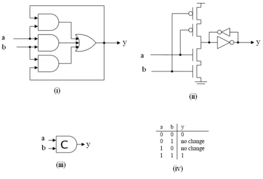
(22) 2.3 Balsa Back-End The Balsa back-end generates gate level netlists ready for being imported into target CAD systems to yield circuits implementations. In this section we are going to introduce some basic cells tuned for Xilinx technology which are generated by Balsa, such as Muller C element and S element. We will also describe some handshake components (5) in Balsa synthesis system. 2.3.1 Basic Elements The gate level netlist generated for Xilinx technology by Balsa only makes use of some basic cells including AND, OR, NOR, XOR, NADN, BUF, XNOR, INV, FD (Dtype flip-flop), FDC and FDCE. Basic elements are built from these cells.. Figure 12 : The Muller C-Element as (i)Gate-Level Implementation, (ii)TransistorLevel Implementation, (iii)Logic Symbol, (iv) Truth Table Shown in Figure 12, the Muller C-element is a commonly used asynchronous logic component originally designed by David E. Muller. The output of the C-element 13.
(23) reflects the inputs when the states of all inputs match. Simply put, the output is set to 0 when all inputs are 0, and it is set to 1 when all inputs are 1. The other input permutations just do not alter the output, when the element serves as a state holder much like an asynchronous set-reset latch. Combining this with the observation that all asynchronous circuits rely on handshaking that involves cyclic transitions between 0 and 1, it should be clear that the Muller C-element is indeed a fundamental component that is extensively used in asynchronous circuits.. 14.
(24) Figure 13 : The NC2P-element as (i) Logic Symbol (ii) Truth Table (iii) Gate-Level (iv) Transistor-Level Implementation Figure 13 shows the NC2P element. Output is set to 1 as long as a is 0, regardless of b value. It resembles C-element very much in the NMOS or lower part of the circuit, while the output assumes the opposite signal. The only permutation left just keeps the original state. It may look weird at this point, however, we will have use for this in the upcoming element.. 15.
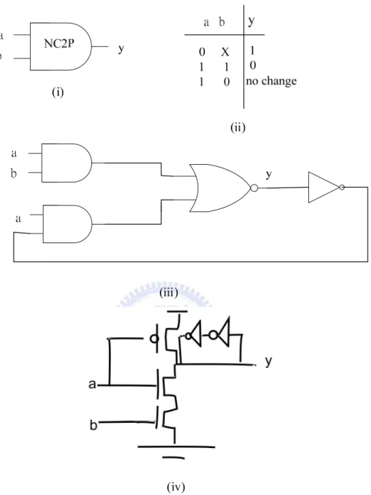
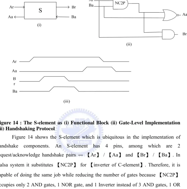
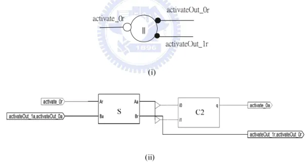
(25) Figure 14 : The S-element as (i) Functional Block (ii) Gate-Level Implementation (iii) Handshaking Protocol Figure 14 shows the S-element which is ubiquitous in the implementation of handshake. components.. An. S-element. has. 4. pins,. among. which. are. 2. request/acknowledge handshake pairs ― 【Ar】 / 【Aa】 and 【Br】 / 【Ba】. In Balsa system it substitutes 【NC2P】 for 【inverter of C-element】. Therefore, it is capable of doing the same job while reducing the number of gates because 【NC2P】 occupies only 2 AND gates, 1 NOR gate, and 1 Inverter instead of 3 AND gates, 1 OR gate, and 1 Inverter by【inverter of C-element】.. 16.
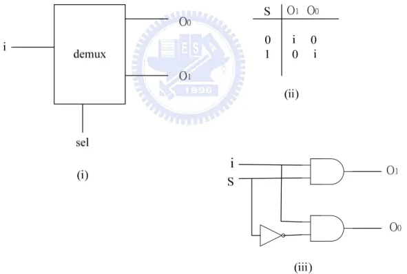
(26) Figure 15 : The Multiplexer as (i)Logic Symbol (ii) Truth Table (iii) Gate-Level Implementation. Figure 16 : The De-Multiplexer as (i) Functional Block (ii) Truth Table (iii) GateLevel Implementation Figure 15 and 16 show separately the multiplexer and de-multiplexer elements. They are used extensively in many components such as Balsa full adder and BrzCase.. 17.
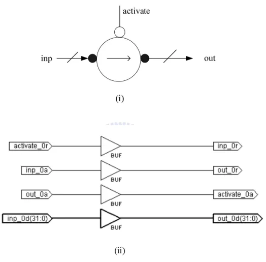
(27) 2.3.2 Handshake Components The handshake component sets used by Tangram(1) and Balsa are very similar. Balsa contains about 40 components that signal handshakes for communication, each of which has a substantial gate-level implementation associated. We will illustrate some handshake components in the following to shed a bit light on their mechanism.. Figure 17 : The Fetch Component as (i) Symbol (ii) Gate-Level Implementation Shown in Figure 17 is the Fetch component which is the most common way to control a datapath from a control tree. Transferrers are used to implement assignment, input and output channel operations in Balsa by transferring a data value from a pull datapath and by pushing it towards a push datapath.. 18.
(28) Figure 18 : The Sequence Component as (i) Symbol (ii) Gate-Level Implementation. Figure 19 : The Concurrent Component as (i) Symbol (ii) Gate-Level Implementation Sequence and Concur in Figure 18 and 19 form a large part of handshake circuit control trees. They are used to activate a number of commands under the control of the activate handshake.. 19.
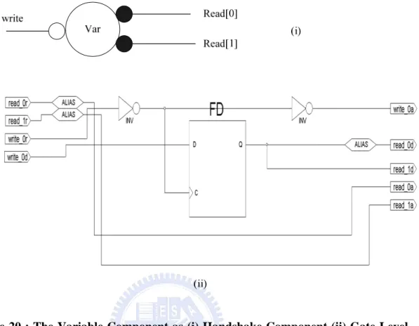
(29) Figure 20 : The Variable Component as (i) Handshake Component (ii) Gate-Level Implementation The variable component in Figure 15 uses D-type flip-flop to store data. The source of pulse triggering storage comes from the signal write_0r. When a certain piece of data should be stored, write_0r will be pulled up and down to trigger the flip-flop, in the meantime signaling acknowledgement write_0a. Likewise, when the data is desired read_0r or read_1r is set, followed by read_0a or read_1a. The compilation mechanism for HDLs must ensure that activity on the write port and read ports are mutually exclusive.. 2.4 Concluding Remarks In this chapter we introduced the ISO10918-1(2) specifications, known widely as JPEG. We walked the reader through the three main stages constituting JPEG encoding/decoding processes. They are entropy coding, quantization, and DCT operation. We learned that if we are to design a JPEG decoder architecture much of the efforts should be focused on Huffman decoding, and a lot more on IDCT unit.. 20.
(30) Then we introduced. the. classification of the asynchronous circuits.. Asynchronous circuits can be classified into SI, DI, QDI, or ST according to the delay assumptions. Lastly we illustrated the Balsa back-end with symbols and gatelevel/transistor-level implementations. Balsa synthesis system consists of approximately 40 components, each of which can be translated to gate-level netlist. Those components make use of handshaking protocol for communication.. 21.
(31) 3. Designing the JPAD Knowing that it’s not quite appropriate to get down to details just yet, we shall take a rough view at the architecture of JPAD for starter. After being somewhat familiar with its directions of dataflow, we shall closely explore each functional block and even reveal a few lines of code to help understanding of the algorithms. Eventually we will discuss the speedup already done and theoretically possible future optimizations.. 3.1 JPAD overview. Figure 21 : The Architecture of JPAD From a general view at JPAD we know it consists of a control unit, a BSU( bit supply unit ), a Huffman decoder, an IDCT unit, a dequantizer, an extender, a register file, a RAM, and a ROM. Arrowed buses and lines stand for channels and thus transfers. 22.
(32) of data as well as their directions. Purple arrowed lines mean that the control unit has control over their destination blocks. After the virtual RAM finished loading file to it, the BSU runs parallel to the control unit until either one terminates. The idea is as follows: the control unit requests data from BSU, asking for certain number of bits, instead of getting it directly from RAM. It is BSU that fetches the data from RAM whenever it is empty. The control unit will then send data and commands to the Huffman decoder, which further sends the decoded index to the register file. Once the indexed value is analyzed and part of it extended, the quantized DC/AC component goes to the register file. After the essential DC/AC components are dequantized and stored back again to the register file, IDCT takes charge and calculates/restores the original pixels. Because the reordering and upscaling are unneeded in visualizing the results, the IDCT unit simply outputs to file each time it completes an 8x8 arithmetic block. When the end of file is reached, the whole DSP halts.. 3.2 Dissecting JPAD 3.2.1 Bit Supply Unit Since the control unit can ask for different numbers of bits from 1 to 16, it’s necessary for the BSU to keep track of which bit is read last time.. Figure 22 : Partial Code of BSU 23.
(33) As written in Figure 22, the position tracker curBit assumes a value between 0 and 16. Whenever it reaches 16, memory is read, the address counter curAddress is incremented, and curBit is reset. As soon as temp is appended enough bits, the loop is quit and the value of temp is relayed to the output channel, finishing the transaction. Something worth noting is that during entropy decoding, in order to ensure that a marker does not occur within an entropy-coded segment, any X’FF’ byte generated by either a Huffman or arithmetic encoder, or an X’FF’ byte that was generated by the padding of 1-bit, is followed by a “stuffed” zero byte. In other words, should X’FF’ appear during entropy encoding, it must be replaced with X’FF00’ to remove ambiguity. Therefore it takes special care to modify the BSU.. Figure 23 : Partial Code of BSU – Continued The trick is to add a flag that indicates the validity of the future X’00’ encountered. X’00’ will just be neglected if the flag is false, or be processed as usual if the flag is true. Also due to the fact that X’FF00’ may span across 32 bits, we cannot keep only 16 bits at one time. Therefore we added nextData, which is next data to come after curData is depleted. 3.2.2 Huffman Decoder In the JPEG mode we will be using in this thesis, the possible Huffman values are the integers 0 to 255. It is known that depending upon how the Huffman coding algorithm is applied, different codes can be generated from the same symbol values and frequency data. The JPEG standard does not specify exactly how Huffman codes are generated. Actually, the Huffman codes for values in JPEG files do not have to be optimal. Table 1 : Count of Code Lengths for AC Component 1 24.
(34) Code Length 1 2 3 4 5 6 7 8. Count 0 2 1 3 3 2 4 3. . . .. . . .. Table 1 lists how many codes there are for each length. It is part of the default Huffman table suggested for baseline JPEG. The obvious method for decoding Huffman values is to create a binary tree containing the values arranged according to their codes. Start at the root of the tree and, using the value of bits read from the input stream to determine the path, search for the value in the tree. A simpler method to implement is to use the list of values sorted by Huffman code in conjunction with an array of data structures with one element per Huffman code length. Each structure contains the minimum and maximum Huffman code for a given length and the index of the first value with a Huffman code of that length in the sorted value array. Table 2 : Huffman Decoding Data Length. Minimum Code. Maximum Code. First Value. 1 2 3 4 5 6 7 8. N/A 00 100 1010 11010 111010 1111000 11111000. N/A 01 100 1100 11100 111011 1111011 11111010. N/A 1 3 4 7 10 12 16. 25.
(35) With predictable Huffman tables like that in Table 2, it is natural to hardwire/pre-store those values in the ROM and calculate the original values by the algorithm below.. Figure 24 : Code Snippet of Huffman Decoder The upper region looks for proper code length to start with. Once there is a match, which is detectable by comparing the target code with the minimum code, the decoded index will be sent to the output channel. The index is attainable by subtracting minimum code from the target code, which yields an offset, then by adding the first index value of that length. In the end, I made 4 versions of this corresponding to all possible Huffman tables ever found in pure baseline JPEG. 3.2.3 Extender In the previous chapter we mentioned the symbol pair (SIZE, AMPLITUDE). In order to restore its value we still have to send it into the extender and perform some simple computations.. 26.
(36) Figure 25 : Magnitude Codes and Ranges Figure 25 gives us some clue as to which magnitude represents what range of numbers. It is quite apparent that the closer it is to the origin the smaller magnitude it has and hence the fewer bits it occupies. To reveal how they convert we would borrow some lines from my code.. Figure 26 : Partial Code of Extender 27.
(37) First we would shift vt whose initial value is 1 leftwards by (size – 1) bits, then compare the additional bits with vt. If the additional number is greater than vt, it is taken as output and we know it’s positive. Otherwise subtract it by vt twice and add a one so it is negative. Take B”11” for example, since 11 is larger than 10, it translates to +3. Likewise, since B”00” is smaller than 10, it makes a -3. 3.2.4 Dequantizer This is by far the most trivial component in the whole JPAD. It’s no big deal but a booth multiplier, so we will just skip it for now. 3.2.5 Control Unit The control unit is the thinking brain that issues all commands to its minions. It is also the only component dealing with markers or tags. The JPEG header is a messy tangle, and it deserves full attention when being handled.. Figure 27 : Structure of a JPEG File 28.
(38) All of the markers are represented by 2 bytes, starting with X”FF”. The SOI marker (X”FFD8”) marks the beginning of an image. Well, since all image files have X”FFD8” at the very top of them, it can be skipped without any doubt. The next adjacent JFIF marker (X”FFE0”) stores a lot of information from “JFIF” string, version, units, density, to thumbnail. Ironically, since we know what we are doing, we have no use for them either. The next Define Quantization table (DQT) marker (X”FFDB”) records a quantization table mandated by the dequantization process and should be processed.. Figure 28 : A Code Snippet searching for X”FFDB” from Control Unit The 2 lines req <- reqInfo and streamData -> curData are the standard procedure throughout the code to fetch data from BSU. The loop appends 8 bits to temp each time it receives data until X”FFDB” is found. This way it is convenient to locate a certain marker within the file, and to skip desired number of bits as well.. Certainly we. shouldn’t forget to store the tables too.. Figure 29 : A Code Snippet writing 64 values to quantization table After storing what is necessary and discarding what’s not, we are ready to jump to the Start of Scan (SOS) marker (X”FFDA”) and commence entropy decoding.. 29.
(39) Figure 30 : A Code Snippet performing Huffman DC decoding Figure 30 explains the way control unit calls Huffman decoder. Temp is appended one bit at a time and transferred to Huffman decoder to determine if there is a hit. If there is a match, we can use “index” together with the Huffman table to find its code value, otherwise “index = 255” will inform us there is no match and the loop continues. For a DC coefficient the decoded code value can be sent to extender and the real DC value will be derived. Unlike a DC one, for an AC component the run length is extracted from the 4 higher bits of the decoded code value and the size is extracted from the lower 4 bits. The DC/AC components, whether zero or non-zero, are placed in the array in a zig-zag order. The sequence is indexed by pre-stored table just like min-max of Huffman.. 30.
(40) Figure 31 : Indexable Zig-Zag Sequence When all 64 components are filled, it’s time to move them into the IDCT unit and wait for the results.. 3.3 Make the Common Case Fast Everyone familiar with Computer Architecture knows painfully well about Amdahl’s law. The law is used to find the maximum expected improvement to an overall system when only part of the system is improved. From our experience and cognition, most of the computing time is spent on IDCT calculation. Even the Huffman decoding process is intrinsically a downward matter. The following codes are indecipherable until the precedent ones are decoded. As a consequence, all the struggles should be put on IDCT and on it only for the sake of performance. At the time being there are generally two tactics tackling IDCT, one of which is butterfly(6) and the other is without butterfly. If the butterfly is exploited to full extent, the number of multiplications can be drastically reduced, for the cost of more additions and more time. Bearing in mind no matter how hard we manage to reduce multiplicative operations, there are still inevitable ones over there.. 31.
(41) Since the speed of a pipeline is determined by the slowest stage within, the optimal speed is restricted to the time of a single multiplication. In Jari Nikara’s paper(7)(8) he introduced a pipeline structure that is divided by 3 sets of multipliers evenly placed. This is exactly what we are looking for ― each stage is accompanied by 4 or 5 multipliers running in parallel.. Figure 32 : The 3 Pipeline Stages of IDCT As shown in Figure 32, the 8 inputs X0 ~ X7 flow from the left to the right, eventually transforming into 8 results x0 ~ x7. We then encapsulate the 3 stages with an outer module IDCT, to facilitate connection with other modules and to improve its modularity.. 32.
(42) Figure 33 : 3 Stages connected in parallel One thing to pay attention to when using the module is that during the first 2 cycles of feeding the data, the outputs are far from ready, yet we have to access them lest a deadlock be caused.. Figure 34 : Data flow diagram of IDCT The strategy is to ignore the data obtained at the first 2 cycles and continue to get them until 8 rows or 8 columns are completed. Applying this simple pipeline structure can give us 3*8/10 = 2.4X speedup versus a non-pipelined approach. If more sophisticated pipelining is desired, more registers or RAM cells must be included to reduce bubbles and increase throughput to achieve an ideal 3X improvement for the IDCT part.. 33.
(43) 4. Implementation and Verification This relatively short chapter consists of three parts. First we will illustrate our design flow for asynchronous implementation based on FPGA and VLSI. Then we will point out several issues and problems circling Balsa synthesis. Finally we will explain how we verify our design.. 4.1 The VLSI and FPGA design flow for asynchronous circuit using Balsa The JPAD core is modeled with Balsa language, and then compiled into a collection of “handshake components” with the balsa-c compiler. Each of these components has a concrete gate level implementation. By using the balsa-netlist tool we can automatically generate them into Verilog for Xilinx or other target synthesis tools. The following steps are the design flow for FPGA. The Verilog netlist generated by balsa-netlist is converted into a netlist of basic gates in the synthesis step of the design flow. The netlist may be optimized using technology-independent logic minimization algorithms. However, we must avoid the logic minimization for hazard free circuits and buffers generated by balsa-netlist. We should add the constraint “keep hierarchy” to avoid the logic minimization. Then the synthesized netlist is mapped to the target device using a technology-mapping algorithm. The placement algorithm maps logic blocks from the netlist to physical locations on an FPGA. Once the placement has been done, the routing algorithm determines how to interconnect the logic blocks using the available routing. The final output of the design flow is the FPGA programming file, which is a bit stream determining the state of every programmable element inside an FPGA. The design flow is shown is Figure 35.. 34.
(44) Figure 35 : The FPGA design flow of Balsa The VLSI design flow of Balsa is somewhat different from that on FPGA. For the first thing, the Balsa-netlist does not support the Synopsys technology. The only thing we may use is the “Example technology”, with some gates modified in the standard cells to adapt for Synopsys. Then we proceed to use Synopsys Design Compiler to synthesize the Verilog model. After synthesis, we can run the functional simulation 35.
(45) with Modelsim. If everything is alright, we may move a step further to do the place and route with SOC Encounter and export the layout GDS file. Balsa description. Balsa-c. Behaviour Simulation. Breeze description. Balsa development kit Balsa-netlist. Netlist for Synopsys Function Simulation ModelSim Synopsys Design Compiler. Gate level netlist. Cadence SOC encounter. Timing Simulation. Layout netlist. Figure 36 : The VLSI Design Flow of Balsa. 4.2 Implementation Issues Compilation from Balsa programs into Xilinx netlists proceeds in two steps. In the first step, handshake circuits are produced to form the intermediate framework. An interesting feature of this compilation is that it is transparent, allowing feedback about important performance characteristics such as performance, area, timing, and so forth to 36.
(46) be created at the handshake circuit level and to be presented to the VLSI programmer at the Balsa level. When the designer is content with the performance of the Balsa program, the corresponding handshaking circuit is then expanded into a gate-level netlist targeted for a certain technology. At this level the design can be simulated to obtain more accurate performance figures with the help of commercial simulators. We chose four-phase bundled data protocol over dual-rail to implement the handshake circuit in order to reduce the area cost. Balsa also provides a few technologies to select from. If we select Xilinx ISE, the circuits are implemented using just the Xilinx standard cells such as AND, OR, Inverter gate and flip-flop. If the target synthesis tools are not supported, like Synopsys Design Compiler, we can use the “Example” technology which translates the circuit to some basic cells, and we have to somehow make them compatible with the standard cells in the target synthesis tool. It should be bewared that the Xilinx synthesis tool could perform logic minimization but it must be avoided. The asynchronous system adds some buffer or redundant circuit to ensure hazard-free, however, minimization is not applicable here. We can avoid this situation by adding the constraint “keep hierarchy” on the handshake modules. RAM is not modeled by Balsa language. We can implement it using the block RAM on FPGA or using the standard RAM in VLSI. A handshake interface between the JPAD core and the memory must be devised if so required.. 37.
(47) 4.3 Verification. Figure 37 : JPAD Behavior Simulation Environment The environment used to do behavior simulation for JPAD is illustrated in Figure 37. The RAM model is the predefined procedures in Balsa as shown in Figure 38.. Figure 38 : Balsa Description for Memory Model We assign the address width and data width to decide their size. For convenience, address width is 2^22 and data width is 2 bytes which yield a total 8MB to accommodate all possible size JPEG files. The contents of the RAM are loaded during initialization as 38.
(48) 16-bit quantities in the hexadecimal format from an ASCII file. An ASCII file is translated from a JPEG file from my own C# program named Hex2ASCII written just for this project.. Figure 39 : User Interface of Hex2ASCII Whenever an address arrives at the RAM model from the RAM address channel along with rNw set to “read”, the RAM outputs the header information or the image data. The photo viewer software, such as ACDSee or Photoshop, offers us options to compare the pictures by bare eyes or to compare uncompressed BMP files converted from JPEG and my own program ASCII2BMP in Figure 40. If the results differ too much, we must go back to modify the code of JPAD.. 39.
(49) Figure 40 : User Interface of ASCII2BMP. 40.
(50) 5. Simulation Result This chapter is organized as follows: We will start by analyzing some pictures we decoded with JPAD. Then we will post the gate counts and area costs calculated from different EDA tools.. 5.1 Accuracy Analysis In general, the fixed-point arithmetic is employed for speed and area efficiency of the design. However, a fixed-point representation introduces an accuracy problem due to the finite word length. Consequently, the signals must be quantized to the given word length and can be represented only in finite precision. From the implementation point of view, the truncation of two’s complement is the cheapest quantization method. Since we took the fixed-point approach in designing the multiplier, errors are likely to surface and should not be overlooked. 5.1.1 PSNR This metric, which is used often in practice, is called peak-to-peak signal-to-noise ratio.. d X, Y. 10 log. ∑. ,. ,. X,. Y,. Generally, this metric is equal to Mean Square Error, but it is more convenient to use because of logarithmic scale. 5.1.2 Samples of PSNR Below we will paste a couple of JPAD-decoded BMP files and their measurements of PSNR with respect to Y, U, and V components in the YUV color space. The first portrait is the worldly known Mona Lisa by Leonardo da Vinci.. 41.
(51) Figure 41 : Mona Lisa. 42.
(52) Figure 42 : Y Component of Mona Lisa 43.
(53) Figure 43 : U Component of Mona Lisa 44.
(54) Figure 44 : V Component of Mona Lisa. 45.
(55) Another iss a wallpapeer of the pop pular Marveel® movie seeries Spiderrman®.. F Figure 45 : Spiderman S n3®. 4 46.
(56) Figure 46 : Y Compoonent of Sp piderman3®®. 4 47.
(57) Figure 47 : U Compoonent of Sp piderman3®®. 4 48.
(58) Figure 48 : V Compoonent of Sp piderman3®® 5.1.3. PSNR in num mbers. However w we want to show all thhe pictures we w picked, it would seeem improp per to do so. Hence we can do nothhing but resort to numeeric figures here. h. 4 49.
(59) Table 3 : PSNR off 6 differen nt pictures in i YUV collor space Y. U. V. bloodelvves. 42.6964. 48.3756. 47.5346. crysis. 42.4501. 49.9767. 50.8844. haruhi. 45.2988. 48.6319. 47.889. monalisa. 45.0897. 49.8218. 48.7581. spiderm man. 45.818. 48.2936. 49.8223. 45.5227. 47.1696. 48.0545. twilight. twilight spiderman m monalisa. V U. haruhi. Y crysis bloodelves 0. 20. 40. 60. 80. 100. Figure 49 : PSNR R Displayed d in Bars v low errror rates. This T kind off data preseentation can n The blue dots represent very be associatted with thaat of thermaal imaging, with whitee color as thhe highest teemperature. A much hiigher PSNR R can be seeen from Figure 50. Siince the resuults are quiite well andd we cannott hardly tell the differrence at all,, we know that the fixxed-point multiplier m iss indeed fauultless and not n worth ann overhaul.. 5 50.
(60) Figure 50 : Official Sample. 5.2 Area Cost We have two sets of figures concerning cost, one of which is based on gate counts, and the other on areas. The gate count numbers are taken from Map Report in Xilinx ISE. The “total equivalent gate count” is an estimate of the number of gates if this design has been implemented with standard-cells. Table 4 : A List of Total Equivalent Gate Counts Gate Count ControlUnit. 441590. IDCT. 158509. Stage1. 50038. Stage2. 42669. Stage3. 42768. Huffman Decoder. 22832. BSU. 8577. Mul. 7018. Dequantizer. 4092. Extender. 2000. 51.
(61) Gaate Coun nt. 8577. 42768. 22832 2. 7018. 4 4092. 000 20 C ControlUnit. 42669. IDCT S Stage1. 8 50038. S Stage2 441590 158509. S Stage3 H Huffman Deco oder B BSU M Mul D Dequantizer E Extender. Figure 51 : Gate Cou unts Displayyed in a Piee Onn the other hand, h the “tootal cell areea” is an estimate of areeas measureed in squaree micrometeers. It is callculated by Synopsis Design D Com mpiler, an inndustry appproved RTL L synthesis tool. t Table 5 : A List of o Total Cell Areas Total Celll Area ControolUnit. 19099812.63. IDCT. 5688211.44. Stage11. 1933338.95. Stage22. 1599384.16. Stage33. 1588403.06. Huffm man Decoder. 1044809.36. BSU. 355198.98. Mul. 244644.55. Dequaantizer. 144643.47. Extender. 9 9722.71. 5 52.
(62) 35198.98 4809.36 104 87927.01 . Totaal Cell A Area 14096.91 1 14643..47 . 9 9722.71 . Unit U : . µm2. C ControlUnit. 88018.68 . IDCT. 1069 934.50 . S Stage1 S Stage2. 314762.47 1527466.50 . S Stage3 H Huffman Deco oder B BSU Mul(16‐bit Ver.) M D Dequantizer E Extender. Figure 522 : Cell Areeas Displayyed in a Pie Froom the two charts we could c infer tthat both Xiilinx ISE annd Design Compiler C doo a good jobb (or bad one) of evaluating the area costs, for they arre so close. To explainn what they have to do with w JPAD,, we have too restate agaain their relaationship. Because both ControlUniit and BSU are the top modules opperating in parallel, p wee can affirm m that they represent r thhe total areaa cost for thhe whole JP PAD circuit.. Moreover, since 1.9M M um isn’t an astronom mical numbber out of human h reachh, we could lie back onn the sofa annd say it’s a viable deesign. Whenn we have more m time iit will be verifiable onn FPGA, or even on a chip c if more crew effortts are granteed. (Afterr the thesiss defense, the t committtee membeers demandded that I modify myy design so that the multiplier m innvolved in IDCT I is reeduced to 16-bit by 16 6-bit. Quitee fortunatelyy, the picturre looked litterally the ssame and thhe cost was even less. The T chart iss pasted beloow as an apppendix.). 5 53.
(63) 35198.98 4809.36 104 87927.01 . Totaal Cell A Area 14096.91 1 14643..47 . 9 9722.71 . Unit U : . µm2. C ControlUnit. 88018.68 . IDCT. 1069 934.50 . S Stage1 S Stage2. 314762.47 1527466.50 . S Stage3 H Huffman Deco oder B BSU Mul(16‐bit Ver.) M D Dequantizer E Extender. Fig gure 53 : Ceell Areas frrom a 16-biit MUL sch heme. 5 54.
(64) 6. Conclusion, Confession and Future Work In the end of the project we successfully designed and implemented JPEG Asynchronous Pipelined Decoder, abbreviated JPAD, with Balsa the asynchronous synthesis tool. The resulting decompressed pictures are nearly indiscernible from those of commercial image viewing application programs. From the performance-oriented viewpoint, a speedup of 2.4X was achieved. Too bad we don’t have an FPGA-ready Modelsim-compatible netlist yet, which is why we don’t have an object to compare it with except our own. Balsa may be very convenient to use in preliminary design phases, however, during post-completion stages the circuit it generates is far from being compact and efficient, plus tedious to tune up. My proposition here is that, for handshake simulation and educational purposes the toolset is quite useful against a manual approach, yet not so for making market-value commercial products. There is much future work left to be done. The proposed pipeline structure still has a lot of room for improvement―that is― to totally remove bubbles and keep its usage at 100%. Most importantly, we have a long bumpy way to go to reach our ultimate goal, the layout. Overall, the thesis offers the following contributions, if not much: z. The architecture of the asynchronous baseline JPEG decoder modeled with Balsa is described. Some design issues for Balsa language is also covered.. z. The design flow for the asynchronous circuit implementation on FPGA as well as VLSI is mentioned.. z. The verification flow is devised, which involves subjective visual inspection and software ratings.. z. A pipeline structure to improve the most time-consuming arithmetic is developed. Some may doubt that those were just pretty words, I myself doubt that too. But. from what I have heard, the authors of Balsa promised that they would do their best to fix the problem as well as add more new features. Have faith, folks!. 55.
(65) References 1. Kessels, J. and Peeters, A. The Tangram framework: asynchronous circuits for low power. 2001. p. 255. 2. Continuous-Tone, Information Technology – Digital Compression and Coding of. ISO/IEC 10918-1 and ITU-T Recommendation T.81. 1993. 3. The JPEG Still Picture Compression Standard. Wallace, Gregory K.;. Maynard, Massachusetts : IEEE Transactions on Consumer Electronics. 4. Davis, Al and Nowick, M. Steven. An Introduction to Asynchronous Circuit Design. 1997. UUCS-97-013. 5. Berkel, K. V. Handshake Circuits. An Asynchronous Architecture for VLSI. 1993. 6. Chen, Wen-Hsiung, Smith, C. Harrison and Fralick, S. C. A Fast Computatonal Algorithm for the Discrete Cosine Transform. 1977. 7. Nikara, Jari, et al. Implementation of Two-Dimensional Discrete Cosine Transform and its Inverse. 2003. 8. Pipeline Architecture for Two-Dimensional Cosine Transform and Its Inverse. Takala, Jarmo, Nikara, Jari and Punkka, Konsta. Tampere, Finland : IEEE, 2002.. 56.
(66)
數據
+7
相關文件
A cylindrical glass of radius r and height L is filled with water and then tilted until the water remaining in the glass exactly covers its base.. (a) Determine a way to “slice”
Reading Task 6: Genre Structure and Language Features. • Now let’s look at how language features (e.g. sentence patterns) are connected to the structure
develop a better understanding of the design and the features of the English Language curriculum with an emphasis on the senior secondary level;.. gain an insight into the
Step 1: With reference to the purpose and the rhetorical structure of the review genre (Stage 3), design a graphic organiser for the major sections and sub-sections of your
(d) While essential learning is provided in the core subjects of Chinese Language, English Language, Mathematics and Liberal Studies, a wide spectrum of elective subjects and COS
Then they work in groups of four to design a questionnaire on diets and eating habits based on the information they have collected from the internet and in Part A, and with
Students are asked to collect information (including materials from books, pamphlet from Environmental Protection Department...etc.) of the possible effects of pollution on our
Then, we tested the influence of θ for the rate of convergence of Algorithm 4.1, by using this algorithm with α = 15 and four different θ to solve a test ex- ample generated as
