(Received March 1, 2000; accepted July 27, 2000) 1328
INTRODUCTION
In response to the Pb-free trend in the electronic industry, many efforts have been made to develop Pb-free solders, with eutectic Sn-Ag being a prospective alloy.1,2 Compared to Sn-base solders, In-base solders have been shown to possess certain advantageous prop-erties such as better wettability, lower meting point, and longer fatigue life.3,4 As a result, In-Ag solders have also been favored in specific applications where cost is of lesser importance. Chen et al.5 studied the melting and solidification characteristics of In-Ag solders through DSC analysis. Humpston et al.6 have also investigated the spreading and joint filling behavior of In3Ag solder on gold-deposited glass substrates.
In the electronic industry, silver substrates have been widely used in manufacturing thick-film hybrid integrated circuits (HIC), resistors, ceramic capaci-tors and multi-layer chip induccapaci-tors. For a flip chip assembly, silver has also been employed as the wet-ting layer in the field of under bump metallurgy (UBM).7 The interfacial reactions of Sn thin-film, Pb-Sn and Pb-Sn-Ag bulk solders with Ag substrates have been investigated by a number of researchers,8–14 and they all showed that the intermetallic compounds formed during these interfacial reactions were of the Ag3Sn phase. In the case of In/Ag interfacial reac-tions, most studies considered thin-film reacreac-tions,
Interfacial Reactions between In10Ag
Solders and Ag Substrates
Y.M. LIU and T.H. CHUANG
National Taiwan University, Institute of Materials Science and Engineering, Taipei, Taiwan, R.O.C.
The morphology and growth kinetics of intermetallic compounds formed during the reaction of liquid In10Ag on Ag substrates in the temperature range between 250°C and 375°C are studied. The results indicate that the Ag2In intermetallic compounds that appear at the interface are in the columnar shape, enveloped by thin AgIn2 shells. The growth kinetics of intermetallic compounds are parabolic, indicating that the reaction is diffusion-controlled. The Arrhenius reaction activation energy was found to be 44.9 kJ/mol. Also, the wetting behavior of the In10Ag on Ag substrates was studied. The results show that there exists a transient plateau of the contact angle variation. Such a phenomenon can be explained by the intermetallic compound precursor halo formation preceding the edge of the solder drop.
Key words: In10Ag solder, Ag substrate, intermetallic compound, wettability
rather than the soldering aspect. In the study of the interfacial structures of InP/Ag thin-film contacts, Mills et al.15 showed that the AgIn
2 phase precipitates out as a secondary phase during the slow cooling process after annealing. With respect to the In/Ag thin-film coupling reaction, Simic et al.8–10 reported that Ag2In compounds form when the In/Ag thickness ratio decreased below 1.44 (50 wt.%In), vis-à-vis the formation of AgIn2 compounds at an In/Ag thickness ratio of 1.44 and greater. The formation of AgIn2 and Ag2In was diffusion-controlled, and the growth rate of Ag2In was one order of magnitude lesser than that of AgIn2. After lengthy exposure at room temperature for 15 years, the intermetallic compounds (AgIn2 and Ag2In) formed at the In/Ag thickness ratio of more than 0.51 (26 wt.%In) remain stable, while samples with intermetallic compounds with In/Ag thickness ratio between 0.18 and 0.51 decompose to crystalline silver and In2O3 oxides. Kepper et al.16 studied the growth kinetics of AgIn2 in In/Ag thin-film couples by applying the perturbed γ-γ angular correction method, affirming that AgIn2 formation was diffusion-con-trolled and the activation energy was approximately 0.46 eV. In an article by Roy et al.,17 the formation of AgIn2 in In/Ag thin-film couples was also diffusion-controlled, and the activation energy was approxi-mately 0.43 eV in the temperature range of 45–128°C. The AgIn2 phase forms first, and gradually trans-forms into Ag2In phase in the case of Ag-rich films. Bernstein18 showed that in the coupling of In thin
AgIn2 phase formed at temperatures between 157°C and 166°C, while the Ag2In and Ag3In phases appear at temperatures between 166°C and 281°C.
From the research results of In/Ag thin-film reac-tions outlined above, both AgIn2 and Ag2In compounds primarily form on reaction. Secondly, the AgIn2 phase is always the first intermetallic compound formed, and gradually transforms into Ag2In phase for Ag-rich films. The intermetallic compound formation during the solid-solid thin-film reaction is predomi-nantly controlled by the diffusion of In into Ag films. This study focused on the interfacial reactions be-tween In10Ag solder and Ag substrates. For this purpose, the morphology and growth kinetics of metallic compounds formed at the In10Ag/Ag inter-face during soldering reactions at temperatures be-tween 250°C and 375°C are investigated. In addition, wettability is an important property for solders, so the contact angles of liquid In10Ag on Ag substrates are also measured using the sessile drop method. Based on metallographic observations, a mechanism for the wetting behavior is proposed.
EXPERIMENTAL
Ag substrates with a dimension of 8 mm × 12 mm were cut from a 1 mm-thick Ag plate (Ag-99.95 wt.%), ground with SiC paper, and polished with 1 µm and 0.3 µm Al2O3 powders. The In10Ag solders were pre-pared, by vacuum melting then rolling the materials into a foil 0.2 mm thick. For the study of interfacial reactions, the In10Ag solder foil was placed on the Ag substrate and heated in an infra-red furnace under a vacuum of 10-3 torr. The heating processes were con-ducted in temperatures between 250°C and 375°C with the heating time from 5 min to 40 min. Through a water cooling system installed within the furnace, the specimens were cooled to room temperature in two minutes.
For the observations of morphology of the interface after soldering reactions, optical microscopy (OM) and scanning electron microscopy (SEM) were used. The specimens were cross-sectioned, ground with SiC paper, and polished with 1 µm and 0.3 µm Al2O3 powders. The chemical composition of intermetallic compounds formed after reactions were analyzed by an electron-probe microanalyzer (EPMA). For growth kinetics analyses, the thickness of intermetallic com-pounds formed for various temperatures and time periods was calculated through dividing the total area of interfacial intermetallics by the width of these intermetallics on the micrograph. In order to clarify the reaction mechanism, a thin film of Ta with a thickness of about 1000 Å was sputtered across the surface of the Ag substrate. Ta is a diffusion barrier because it does not react with In or Ag.
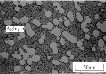
Fig. 1. The microstructure of as-cast In10Ag solder.
The sessile drop method was used to evaluate the wettability of In10Ag solders on Ag substrates in an IR furnace under a 10–3 torr vacuum. Prior to testing, the solder was dipped in a mildly activated rosin flux (RMX). The contact angles were measured in-situ by a video system during heating. SEM observations of the cross-section of the solder drop on the Ag substrate would reveal the mechanism for the wetting behavior.
RESULTS AND DISCUSSION
The microstructure of the as-cast In10Ag solder is shown in Fig. 1. A large number of coarse clusters are embedded in the In3.2Ag eutectic phase. As analyzed by EPMA, the coarse clusters were in the AgIn2 phase. The In3.2Ag eutectic phase consisted of a pure In matrix with a fine dispersion of narrow AgIn2 strips. Figures 2 and 3 show the typical morphology of interfa-cial intermetallic compounds formed between the In10Ag and Ag. The compositions of the compounds, as analyzed by EPMA, are listed in Table I. Initially, a continuous layer of scallop-shaped Ag2In compounds enveloped in thin AgIn2 shells appeared at the In10Ag/ Ag interface. With an increase in reaction time and temperature, Ag2In compounds grew in columnar form into the interior of the In10Ag solder, while the thickness of AgIn2 shells remained at about 0.5 µm to 1.0 µm. Referring to the Ag-In phase diagram, AgIn2 shells result from the reaction between Ag2In com-pounds and the liquid In10Ag solder during cooling. Accompanying the interfacial reaction between the In10Ag solder and the Ag substrate, a cluster of Ag2In islands surrounded by AgIn2 shells also appeared in the interior of the In10Ag solder matrix. As shown in Fig. 4, the Ag2In islands changed from a spherical shape to a dendritic shape at the increase of the reaction time. These compounds were caused by the precipitation of excess Ag from two different sources: Ag originally contained in the In10Ag solder, and Ag dissolving from the Ag substrate into the liquid In10Ag solder during the soldering reaction.
A Ta thin film sputtered on the partial surface of the Ag substrate was used as a diffusion marker. From Fig. 5, the In10Ag(1)/Ag(s) interface slightly formed a sunken curvature in the area adjacent to the Ta
Fig. 2. Morphology of intermetallic compounds formed at the In10Ag(1)/Ag(s) interface after soldering reactions at 300°C for (a) 5 min, (b) 10 min, (c) 20 min, and (d) 30 min.
a b c d
marker, which implies that only less Ag is dissolving from the Ag substrate into the liquid In10Ag solder. Figure 5 also shows that the products of interfacial reaction grew primarily towards the In10Ag solder indicating that the formation of intermetallic com-pounds was dominated by the diffusion of Ag into the solder matrix through the intermetallic compounds. In addition to the formation of intermetallic com-pounds at the interface, some of the Ag in the sub-strate dissolved into the liquid solder. However, in the
present In10Ag/Ag system only about 2% of the Ag in the consumed substrate was found to dissolve into the In10Ag matrix. The result is contrary to that in an In/ Ag system, which showed a large amount of Ag (about 78% of the consumed Ag substrate) dissolved into the liquid In solder.
For kinetics analysis, the thickness (∆x) of the interfacial Ag2In compound versus the square root of the reaction time (t1/2) is plotted in Fig. 6. The error of measurements is between 0.21 µm and 2.33 µm. The
Fig. 3. Morphology of intermetallic compounds formed at the In10Ag(1)/Ag(s) interface after soldering reactions at various temperatures for 30 min: (a) 250°C, (b) 275°C, (c) 325°C, and (d) 350°C.
Table I. EPMA Analyzed Chemical Composition of the Intermetallic Compounds Formed in the Ag/In10Ag Soldering Reaction
Specimens Positions I.M. Phases Ag (at.%) In (at.%)
275°C In10Ag/Ag interface scallop-shaped I.M. 66.63 33.36
10 min I.M. shell 33.09 66.91
In10Ag solder matrix islands I.M. 66.58 33.42
I.M. shell 32.77 67.23
275°C In10Ag/Ag interface scallop-shaped I.M. 66.54 33.46
30 min I.M. shell 33.39 66.61
In10Ag solder matrix islands I.M. 66.41 33.59
I.M. shell 33.29 66.71
325°C In10Ag/Ag interface scallop-shaped I.M. 66.45 33.56
10 min I.M. shell 32.27 67.33
In10Ag solder matrix islands I.M. 66.28 33.72
islands I.M. shell 32.75 67.25
325°C In10Ag/Ag interface columnar I.M. 66.74 33.26
30 min I.M. shell 32.75 67.25
In10Ag solder matrix islands I.M. 66.68 33.32
I.M. shell 32.94 67.06
375°C In10Ag/Ag interface scallop-shaped I.M. 66.86 33.14
10 min I.M. shell 33.67 66.33
In10Ag solder matrix islands I.M. 66.82 33.18
I.M. shell 33.34 66.66
375°C In10Ag/Ag interface columnar I.M. 66.88 33.12
30 min I.M. shell 32.82 67.18
In10Ag solder matrix islands I.M. 66.88 33.12
I.M. shell 33.31 66.69
plots in Fig. 6 are linear indicating that the growth of interfacial Ag2In compounds is diffusion-controlled. From the Arrhenius plot of reaction constants (Kp) (where Kp = ∆x2/t as shown in Fig. 7), the growth activation energy (Q) of interfacial Ag2In compounds is calculated to be 44.9 kJ/mol. The activation energy of lattice diffusion of Ag in bulk In is 53.6 kJ/mol 21 and that of In in bulk Ag is 175.0 kJ/mol.22 This implies that during interfacial reaction between In10Ag sol-ders and Ag substrates, the growth of intermtallic compounds was predominantly controlled by the dif-fusion of Ag into the In10Ag solders, consistent with the morphology observations in Fig. 5.
To estimate the wettability of liquid In10Ag solders on Ag substrates, the contact angles were measured using the sessile drop method at various tempera-tures, as shown in Fig. 8. It was found that the contact angles of all specimens reduced rapidly as the In10Ag solders began to melt and then reached a transient
Fig. 4. Morphology of intermetallic compounds formed in the solder matrix after interfacial reactions between an In10Ag solder and an Ag substrate at 300°C for 30 min.
Fig. 5. Evidence of the growth of Ag2In intermetallic compounds from the original interface into the In10Ag solder matrix. The original interface was marked by a Ta diffusion barrier.
Fig. 6. The linear relation between the average thickness (∆X) of interfacial Ag2In compounds and the square root of time for the In10Ag(1)/Ag(s) interfacial reactions at various temperatures.
Fig. 7. Arrhenius plot of the growth rate constants (Kp) of Ag2In intermetallic compounds formed after the interfacial reactions.
Fig. 8. Continuous measurements of contact angles (θ) for the In10Ag solder drop wetted on Ag substrates at various temperatures.
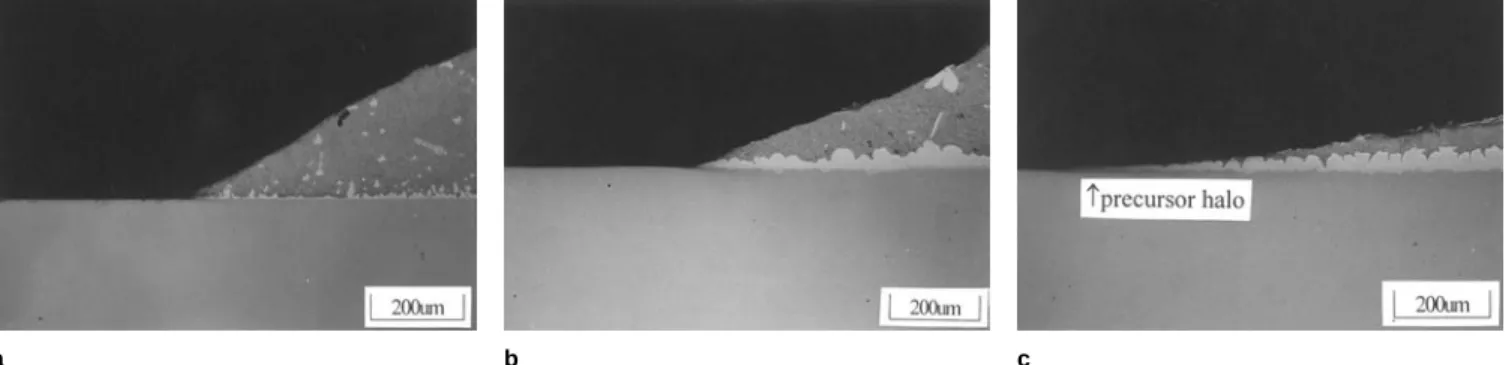
plateau. After a period of time, the solder drop col-lapsed and the contact angles declined to a value near zero. The intervals and heights of the transient pla-teaus on the contact-angle curves decreased with an increase in reaction temperature. In a previous ar-ticle,23 such a wetting behavior was also found in the interfacial reactions between In solders and Au-de-posited substrates, wherein a mechanism was pro-posed to explain the transient plateau phenomenon on the curves of the contact angles measured for liquid In on Au-deposited substrates, and, was further evidenced through SEM observations of the cross section of the liquid drop during wetting. The present study ex-plored whether this behavior also occurred for In-Ag solders on Ag substrates. Figure 9a shows that as the In10Ag solders melt, the drastic decline of contact angles changes to a quasi-stable value, similar to the transient plateau on the wetting curves in Fig. 8. As the intermetallic compounds form and grow at the inter-face of In10Ag solder drop/Ag substrate, a thin film of solder spreads out of the liquid drop and reacts with the Ag substrate to form a precursor halo of intermetal-lic compounds (Fig. 9b). When the intermetalintermetal-lic halo grows to a sufficient thickness, it changes the surface energy of the Ag substrate ahead of the edge of the liquid solder drop, resulting in a further reduction of the contact angle to an equilibrium value (Fig. 9c).
CONCLUSIONS
During the soldering reaction between an In10Ag solder and a silver substrate at temperatures ranging from 250°C to 375°C, Ag2In intermetallic compounds surrounded by AgIn2 thin shells form at the In10Ag/ Ag interface. With an increase of reaction time and temperature, the Ag2In intermetallic compounds change morphology from a scallop form to a columnar shape, while the thickness of AgIn2 shells remains unchanged. The growth of interfacial Ag2In com-pounds is parabolic, indicating that the reaction is diffusion-controlled. The activation energy calculated is 44.9 kJ/mol, near that of the lattice diffusion of Ag in bulk In (53.6 kJ/mol), implying that the growth of interfacial Ag2In compounds in the soldering reaction is dominated by the diffusion of Ag into In10Ag solders. The result can be confirmed by the observa-tion of the growth of Ag2In into the InAg solder matrix
Fig. 9. SEM observations of the cross section of the In10Ag solder drop on an Ag substrate during the wetting process at (a) 300°C, 7 min (the initial wetting stage, with the collapse of the solder drop); (b) 300°C, 40 min (the quasi-stable stage, with the formation of a precursor halo); and (c) 300°C, 120 min (the final wetting stage, with a further outspreading of the solder drop to an equilibrium contact angle).
from the original interface marked by a Ta thin film. The wettability test shows that the contact angles of the In10Ag solder drop first drastically reduce to a quasi-stable value and remain there for a short period of time, and, eventually, decline further to an equilib-rium value near zero. The existence of such a tran-sient plateau of the contact angle can be explained by the formation of a precursor halo of intermetallic compounds preceding the edge of the solder drop.
ACKNOWLEDGEMENT
a b c
The authors would like to thank the National Sci-ence Council (NSC), Taiwan, for the sponsorship of the research project series on the development of Pb-free solders for advanced electronic packaging.
REFERENCES
1. J. Glazer, Int. Mater. Rev. 40, 65 (1995).
2. N.C. Lee, Solid Surf. Mount. Technol. 26, 65 (1997). 3. C.E.T. White, Adv. Mater. Proc. 69 (1986).
4. K. Shimizu, T. Nakanishi, K. Karasawa, K. Hashimoto, and K. Niwa, J. Electron. Mater. 24, 39 (1995).
5. S.W. Chen, C.C. Lin, and C.M. Chen, Metall. Mater. Trans. A, 1965 (1998).
6. G. Humpston and D.M. Jacobson, GEC J. Res. 8, 145 (1991). 7. T. Kawanobe, K. Miyamuto, Y. Inabe, and H. Okudaira,
Proc. IEEE 31th Elec. Comp. Conf. 149 (1981).
8. V. Simic and Z. Marinkovic, Thin Solid Films 61, 149 (1979). 9. Z. Marinkovic and V. Simic, Thin Solid Films195, 127 (1991). 10. V. Simic and Z. Marinkovic, Thin Solid Films 209, 181
(1992).
11. X.H. Wang and H. Conrad, Scrip. Metal. Mater. 31, 375 (1994).
12. C.J. Thwaites and M. Woodall, Brazing and Soldering 12, 57 (1987).
13. Y. Moriya, Y. Yamade, and R. Shinya, IEEE Trans. on
CPMT, part B, 21, 394 (1998).
14. G.Y. Li and Y.C. Chan, Phys. Stat. Sol. 166, R13 (1998). 15. J.S.K. Mills and D.L. Kerk, Thin Solid Films 55, 149 (1978). 16. W. Kepper, R. Wesche, T. Klas, J. Voigt, and G. Schatz, Thin
Solid Films 143, 201 (1991).
17. R. Roy and S.K. Sen, Thin Solid Films 197, 303 (1991). 18. L. Bernstein, J. Electrochem. Soc. 113, 1282 (1966). 19. Y.C. Chen, W.W. So, and C.C. Lee, IEEE Trans. Comp. Pkg.
Manuf. Technol. 20, 46 (1997).
20. D.M. Jacobson and G. Humpston, Solid Surf. Mount. Technol. 10, 27 (1992).
21. T.R. Anthony and D. Turnbull, Phys. Rev. 151, 495 (1966). 22. V.N. Kaygorodov, Y.A. Rabovskiy, and V.K. Talinskiy, Met.
Metallogr. 24, 78 (1967).