i ~'' !j,
ELSEVIER Thin Solid Films 290-291 ( 1996l 176-180
Enhanced electron emission from phosphorus- and boron-doped
diamond-clad Si field emitter arrays
T.K. Ku ~, S.H. Chert b, C,D, Yang ~, N,J, She h, F,G. Tarntair ~, C.C. Wang o, C.F, Chen b
I.J. Hsieh e, H.C. Chang a
= Departm,em of Electronics Engineering a~ld blstitnte of Eleetroal'es, National Chino r~ng University, H,sinela~, lim~,un ~' bl.rt/ttae ~ Materials S¢~¢ac¢ and El'lllfaeeriag. National Chino Tang University. H.rinchu, Tailwm
¢ DepartmemofUectricalEngineering, Chang,Hun Polyleehn¢c hlstilnte. Hsinehu. Taiwan
Abstract
A new fabrication technology of polycrystalline diamond-clad Si micratips using microwave plasma chemical vapor depos tfion (MPCVD) has been developed to improve the characteristics of electron field emission from the pure Si tips, A uniform and smooth coa ;ing morphology for the diamond-clad Si tips have been achieved. Electron emission currenls of diamond-clad tips are much higher than tho~.e of pure Si tips. Such great improvement is attributed to the lowering of the effective work function in the diamond-clad tips. The effects el phosphorus- and boron-doped diamond-clad Si tips have been also studied in comparison with the undoped ones. The current-voltage characteristics of the undoped diamond-clad lips were further enhanced by the in-site doping of phosphorus or boron due to a higMr electron supplement. Moreover, the P-doped diamond.clad tips show a better field emission performance as compared to the B-doped ones. This difference is surmised to be associated with the higher electron ennductivity and defect densities or P-doped diamond films.
geywordx: Diamond-clad Silicon tips'. Field emission; Field emitter arrays; Effective work fitaction
1. Introduction
Microsized fiela emitter arrays (FEAs) fabricated with advanced micromaehining technology has been intensively progressed as the promising electron sources for vacuum microelectronic devices especially for the ultra-thin itat panel displays [ 1 ]. Other potential applications include microwave devices [2], uttra-speed switches, mierosensors, [31 and microsized intense electron sources. In order to achieve low voltage and high efficiency for cold cathode operation, the tip radius and surface work function of a field emitter should be made as small as possible [4]. Moreover, emission sta- bility is also a ,,ery important issue [5]. Among the various types of FEAs, silicon mierotips have become a very attrac- tive candidate because of two notable advantages. First, they are easy to fabricate using modern iC technology, and second, their tip radius can be easily sharpened to the nanometer range [ 6]. On the other hand, their high work function, low electron conductivity, and poor stability are the major drawbacks of Si FEAs. These drawbacks, however, can be minimizedusing surface coating, Coating of the surface of Si mierotips with various materials to enhance their emission efficiency and stability has been reported [7,8], Most of these reports 0040.6090196t$15 00 (0 1996 Elsevier Science SA. All flglas reserved PI! SOn40-6090 ( 96 ) 09058-2
focused on metals. Reccnlly, there has been an increasing interest in the application of CVD diamond films as the mala- rial of electron emitters or cold cathodes due to the unique electrical properties of diamond: first, hydrogenated-( 111 ) diamond has a negative or at least very small electron affinity, i.e. a very low effective work function; and second, diamond is well known to be one of the most chemically and physically stable materials and has the highest thermal conductivity (20 W era- 1 °C - ~) [9,10]. Hence, fabrication of low-field dia- mond field etnitter arrays has been attempted [ 11-141, and a diode-structured prototype field emission display based on a diamond-like carbon has been demonstrated [ 15].
In order to take the advantage of the diamond ncgafive electron affinity (NEA) property, there must exist a source of electrons either in the conduction band or in a subband with energies near or above the vacuum level. In addition, the conductive channels of electrons are also necessary to induce stable electron emission from the insulating diamond. Zha et al. [13] reported that the defects created additional energy subbands within the band gap of diamond and Ihus contributed electrons for emission at low electric fields. Xu et el. 114] suggested that the graphite inclusions embedded in the diamond film might play an important role for the
I~ K Ku et al. / Thin Soli d Filnu 290--291 (1996) 176- h~0 171
contribution of electron conduction channels. However, the mechanism of electron emission from diamond or other ear- bon films is still not entirely clear, Recently, Okano and Gleason [ 16] reported the electren emission from phospho- rus-doped diamond films on plain Si substrates, showinglow- field emission as compared to boron-doped films. However, the implementation of effeetiw and reliable n-type dopants is still difficult.
In this report, the micresized silicon field emission tips coated with polycrystalline diamond film has been success- fully fabricated and characterized. This study has pointed out that uniform polyerystalline diamond films coated on Si tips by microwave plasma chemical vapor deposition (MPCVD) exhibited better emission characteristics than those merely coaled on plain Si suhstrale. The P-doped and B-doped dia- mond films on Si microtips have also been formed employing in-situ doping technology. Hence, effects of diamond doped
with phosphorus and boron on emission properties were evaluated.
radius about 25 nm are shown in Fig. 2. The aspect ratio of the resultant sharp silicon mieroti~ is about 3 I~m/3 ~m. According to our previous work and other works by Zha et al. [13] and Xu et al. [ 14], the higher defect densities in CVD-grown diamond films are responsible for the enhanced electron emission. Hence, the defective diamond crystalli~s deposited by a higher flow ratio of CHa/CO2 ( > 20130) is preferred. Besides, the low flow ratio also leads to a rough and non-uniform coating morphology on the high curvature tip region. The SEM images shown in Fig, 3(at, 3(b) and 3 (c) show the surface morphology of undoped, P-doped and B-doped diamond-clad $i tips deposited by allow ratio of 20.5 / 30 in a CH4-CO2 gas mixture with no dopant source, a
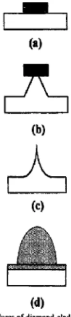
(a)
2. Experimental procedures
A I ~,m thick oxide layer was grown and was photolitho- graphically patterned to form arrays of 50 × 50 circular discs, 3 I~m in diameter, on 2 ~4 ~ em, ( 100)-oriented n-type St substrates. Employing the previously patterned oxide layer as the mask, the cone-shaped Si microtip arrays were subse- quently formed using SFJCI2 reactive ion etching, An oxi- dation-and-stripping process was applied to further sharpen the etched tip to about 25 nm in radius [17]. Before the deposition of diamond, the as-fabricated sharply curved Si microtips were first cleaned by H2 plasma pretreatment and followed by diamond powder (particle size, 0.1 p.m) scratch- ing, In order to grow a continuous diamond film, diamond powder scratching process is necessary to create nucleation sites on the surface of Si substrates, Next, the scratched Si substratcs were dipped into a solution of HF:H20 = I: 100 for a few see ands to remove the native oxide on the silicon, Then diamond films were deposited on the 2 X 2 mm 2 Si snbstrates with a 50×50 tips array using microwave plasma-enhanced chemical vapor deposition (MPCVD) at 850 °(2 ~:ung aCH4- CO2 gas mixture. For the P-doped and B-doped diamond, vapor dopant sources of trimethyl phosphite (P(OCH3)3) and trimethyl borate (B(OCH3)3) were introduced in the diamond deposition [18-20]. The flow rate of P(OCH3)3 and B(OCH3)~ was varied from 0 (undoped) to 0.5 seem when they were introduced to the flow ratios of CH,IICO., of 18 / 30 ~ :20.5/30. The microwave power was set at 450 W and the reaction time was 2 h, The pressure during deposition was 25 Tort. The fabrication procedures are shown in Rg, L
(b)
(e)
I
I
(d)
Fig. 1. Fabrication procedures of diamond-clad St tips', (a) defining oxide mask; (b) Si tips etched by SFa/C[2 RIE; (e) sharpening the etched rips
employing an oxidation-and-strlpping treatment; and (d) diamond film
deposited on the $i tips.
3. Results and discussion
After semi-anlsotropie RIE etching and oxidation sharp- Fig, 2. The vesulls of fon~ing sharp $i micmtiFs with an MIR¢I r~lio of
178 T.K. Ku er aL / Thin S+did Fikmr 290-291 fl996)/7~-180 t" Diamond Shoulder £
~E+', e~.
~ !
Oi=-Sl tip+ 1 Cll41CO~--IO,5/.Kl CH41C0~=10'5130 ~.~Carhoa Moi. Peak 2~o ' 2~o ' ~ ' 2 h '
~ - '
Kinetic Energy (eV)
Fig. 4. Auger electron spectra (AI~S) of andaped. P-doped and B-doped diamond-clad Si lips. The main carbon peak at 272 eV was detected and a either $i nor 0 peaks were detected. A detectable phosphorus peak at around 120 eV was not shown.
Fig. 3. Surface morphologies e[ diam0nd.clad Si lips deposited by a flow ratio of 20.5/30 in CI'14-CO2 gas mixlutes: (a) undoped ones; (b) P-dol~d ones with P(OCl"Is}s=0.2 seem; and (e) B-doped ones with B(OCHsh-0.2 seem.
P(OCHs) 3 flow rate of 0.2 sccm and B (OCHs) z flow rate of 0.2 seem, respectively. To form a continuous and uniform coating, a thicker film (2 ~ 3 I~m} was grown and therefore resulted in a much more blunt shape than the original uncoated $i tip. Both the P-doped and B-doped diamond-clad tips are slightly less in size uniformity compared to the undo- ped ones, as shown in Fig, 3(a)-3(e). This result indicates that the doping proc'ess has no sign i~, .:..at effect on the surface morphology of deposited diamond.
Auger electron spectroscopy (AES) was used to identify the surface compositions of the diamond-clad Si microtips. The AES spectra corresponding to the specimens in Fig. 3 (a) and 3(b) are shown in Fig. 4. In the spectra, the carbon peak
at 272 eV was detected and neither Si nor 0 peaks were detected. The low-energy shoulder around 258 eV in the positive peak of the carbon main peak in the undoped sample, shown in Fig. 3(a), indicated that the surface structure was diamond rather than graphitic or amorphous carbon compo- nents [ 211. As for B-doped samples, their AES ~pectra were similar to those of undoped samples. It reveals that diamond films deposited with a dopant source of B(OCHs) 3 do not significantly change their film property. However, the AES spectrum of the P-doped sample shown in Fig. 3 (b) did not exhibit an obvious shoulder, implying a diamond-like carbon (DLC) nature containing a large amount of graphitie, amor- phous carbon and/or other defects. To simpliFy the descrip- tion, the Si lips coated with diamond lilms under CH4/CO~ flow ratio of 20.5/30 were represented as "Dia-Si tips" in the following description. Moreover, a small phosphorus peak at around 120 eV was detected+ [t indicates that P dop- ,~' 's ,are successfully doped into diamond. According to the .Jaectahle sensitivity of AE$ spectrum, concentration of P dopant is high, in the order of 10 ~v era "~.
Field emission properties of the diamond-clad samples were characterized in high-vacuum environment with a base pressure of about 2.6 × 10- ~o Pa. A schematic diagram ofthe test configuration is shown in Fig. 5. The spacing between a unit emitter array and the graphite collector was controlled at a constant ~ 30 p.m and a unit array contains 50 × 50 tips. When a copper plate instead of the tip array was put on the cathode, a current of less than I nA was measured. Prior to the electrical measurement, a high constant voltage of about 1100 V was applied to the emitters to exhaust the adsorbed
T,K, I¢u er al, / Thin Sotid Filnl,r 290-291 (1996) 176-180 179
...
L
:eVa .~_
tist~cc
Fig. 5, Schematic d iagra m of a high-vacuum fiek[ emission characterization system.
molecule s and evaporate the native oxide. As shown in Fig. 6, the emission current (I~) versus applied voltage (V,) char- acteristics of the P-doped, B-doped and undoped diamond- clad microtips are all superior to that of pa,'e Si microtips, in spite of their relatively blunt curvatures. It is attributed to the lowering of the work fHnetion due to the negative electron affinity of(l I I ) diamond films and/or the much larger effec- tive emission area of the diamond coating. Besides, the sec- ondary electric field enhancement due to the anne-protrusion on the rough diamond-clad tip surface may also be partially
I
f"m'-" ~
tO'~ ,i ''r''r'4m l
../'
/
o ~ e°°2 l e/
~ / " ~ ./ --q~" Undoptd Diu-Si tips ] :,/~u A ~ v " / - --a-- P=O.2 Dia-Si sub. lO"° t / --o:"-B=O.2 Oia-Sisab,I
~ / ~ i --A-- Shup Si tips
,0,q
T
. . .
-'Su"daP°P ; " ~
CO0 700 8DO SlO0 1000 1100 Applied Voltage Va {Y)
Fig, 6, Emission current (l~) versus applied voltage (g.) characteristics of
the P-do~d. B -doped and endoped diamon d-clad tips; the P-d aped. B -dor, cd
~d uedop~d dialnond deposil~d on Si plain snhstratas', and the pure Si lips, The spacing between the emiltcr and collector was a ,'or, slant aboul 311 p,m and the tip number was 2500.
responsible for the emission current enhancement [ 12]. At
V. = 1100 V, a much higher emission current (I,,) of 1,69 m A
for the P-dol~d Din-St tips with P(OCH~)a = 0.2 sccm was achieved, as compared to the 91 p.A for B-doped one with B(OCH))~ = 0.2 seem and only 45 p,A for the undoped one.
Hence, electron emission from the Din-St tips was greatly
enhanced by introducing dopants. P-doped emitters exhibited higher emission currents than B-doped samples for V. > 600 V, In order to evaluate the effects of flow rate of P and B dopant sources on emission current enhancement, one may introduce the "cnhanc:ment ratio" defined as
R~,, = (/d/lo)
where l,t and i. are emission current of doped and undoped Dia-$i tips at a maximum V~ of 1100 V. The value of R~.
represents the degree o f electron emission enhanced by intro-
ducing various dopant concentrations. Fig. 7 shows that the
R~, of Dia-Si tips is significantly dependent on the flow rate of dopant sources. For dopant flow rates beyond 0,05 scorn, the value of /?¢. is rapidly increased with increasing P(OCHO.~ flow rate until R~n reaches a maximum value of 38 at P(OCH3)3 = 0.2 scorn, and R~. is then rapidly dropped to be 3,5 at P(OCH3)3 = 0,5 sectn, as shown in Fig, 7. Thc resistiviLies of the diamood lilmsdoped with P(OCH3) z = 0 2 sccm were measured by the four-point probe method and were tbund to be at least one-order of magnitude lower than those of undoped films. It is believed that tile P-dopants and their associated defect densities increase the energy state den- sities withm the bandgap of the diamond film [22]. Subse- quently, it causes both a higher conductivity and the remarkable enhancement of the electron emission from the P-doped Dia-Si tips, This suggests that the flow rate of P(OCH~)a < 0,05 seem is not sufficientto activatethedoping P impurities and the associated defect densities in the as- deposited diamond films to significantly increase their con-
i
# ,
~--I~O£H~); _._m_ B(OCH)) 1 ~ped ~ a ~ a~ CI1¢/C02-)0,~30 vs.=floor Row b ~ of ~ p = ~ ~u~ets~m)Fig. 7. Enhanrament ratio (Re,} versus doI'~tl source flow rule ¢ltaracc:er- isdcs of doped diamond-dad Si tips,
180 T,l¢, Krt real./Thin SoM FiIm,~ 290.-291 (1996) 176-180 duetivity, However, as a result of the AES analysis shown in
Fig. 5, the quality of diamond film is degraded by introducing P dopants, Although the defective diamond coating is pre- ferred, the as-deposited diamond is degraded to be a fully amorphous sp 2 carbon (a-C) film loosing the NEA property of diamond, if too much P dopant is introduced. The rapidly decreased R.,, of Din-St tips doped under P(OCH~)s=0.5 seem was then attributed to the above phenomenon, There- fore, the dopant concentration of P(OCH~)~ should be opti- mized to achieve the maximum field emission enhancement, As for the B-doped Din-St tips, the flow rate of B(OCH3)3 exhibits little effect on the value of Re. compared to those of the P-doped ones. The R+. of B-doped Din-St tips were slnaller, apart from one exception for doped B (OCH~) ~ = 0.2 seem, It suggest that for the B-doped Dia-Si tips it was nec- essary to introduce a higher B(OCHa)~ concentration for making a significant effect on electron emission, This result is expected since electron emission from n-type semicon- darting diamond is generally preferred. As a result of char- acterization, the P-doped diamond-clad tips show a better field emission performance as compared to the B-doped ones. This difference is surmised to be associated with the higher electron conductivity and defect densities of P-doped dia- mond films. Besides, de, fining F r as the threshold value of the applied field needed to generate a current of 20 gA in our array size with about 0.2 mm 2 (i.e, a typical ~:urrent density of l0 mA em -2 required for effectively exciting a phosphor pixel in a field emission display), the F-r value was reduoed from 33.6 V ~m - i for the undoped diamond-clad tips to 22.3 V I~m- t for the P-doped ones and 30 V Ixm- ~ for the P- doped ones, It indicated the electron emission from P-doped Din-St tips shows low-field emission as comparedto B-doped ones. However, it can be seen from Fig, 6, that when the applied voltage V. is <600 V, the 1~ values of P-doped and B-doped are very close, which suggests that their effective work function are similar, Hence, the 1~ difference between P-doped and B-doped diamond films seem to be dominated by the variation of the electron conductivity,
To confirm that the emission was indeed field emission, the currents emitted from plain substrates coated with P- dol~d and undoped diamond layer were also investigated, The emission currents measured at V.= I100 V were only about 1"7 ~A for the former and 760 nA for the latter. This indicates that most of the emission currents are from the diamond-clad tips.
4, Conclusions
In summary, uniform and continuous diamond films have been successfully coated on Si mierotips using the MPCVD technology. The characteristics of emission current against applied voltage for the blunt undoped diamond-clad tips show superior emission at lower field compared to the pure Si tips, It is attributed to the lowering of the work function due to the
negative electron affinity of ( I 11 ) diamond films and/or the much larger effective emission area of the dianmnd coating. The P-doped and B-doped diamond films on Si mierotips have also been formed employing in situ doping technology. Effects of the phosphorus and boron dopants on the emission properties were evaluated. The P-doped diamond-clad tips ~how a better field emission performance as compared to the B-doped ones. This difference is surmised to be concerned with the higher electron conductivity and defect densities of P-doped diamond films.
Acknowledgements
The research was supported in part by the Republic of China National Science Council under Contract No, NSC 84- 2622-E-009-012, Technique support from the National Nasa Device Laboratory of NSC and Semiconductor Research Center of National Chino-Tung University are also acknowledged.
Rcfel'ences
[ I ] P. Vaudaian and R. Meyer, IEEEIEDM Teeh. Dig, { 1991 ) 197, [ 2] C.A, gpindt. C,E. Holland, A. Rosengoeen and L Brodie, .L Vae, gel.
TechnrtL, n i l (1993) 468,
[3] H.H. Basle, J.E. Pogemiller and n.J. Zimmerman, .L Mieromech, Microeng,, 3 (1993) 45,
[4] T, Utsnmi, IEEE Truss, Electrort Dower, 3,~ ( 1991 ) 2275. [5] H.H. Basra, D.W. Jenkins, B.I. Zimmermas and J,E, Pogeiller, IEEE
IEDM T¢¢h, Dig., ( 1991 ) 213,
[6] R,B, Marcus, T,S, Ravi, 1". Gminar, K Chin, W.J. Orris, D.R. Ciarln, C,E, Hunt and J. Trujillo,,4ppl. Phys, Lest, 56 t 1990) 236. [71 H,H. Busta, RR. Shadducek and W, Owls,/EEl:.. Trans. Eleemm
Device, 36 (1989) 2679.
iS] V,Y. Zhimov and E.I, Givatgizov, Z Vac. Sci, TeehuoL, 1112 (1994) 633,
[9] F.J. Himpsnl, I.A. Knupp, J.A. Van Vechlen and DE, Eastman, N;ys. Roy., B20 t 1979) 62*.
[ 10l M,N, Yod~r, in R,E, Clausing el al, (eds.L Diamond and Diamond- Lik* Films and Coatings, Plenum, New York, 1991, p. I t, [ I l ] C, Wang, A. G~cia, D.C. Ingrain, M. Lake and M.E, Kordesch,
Eleetr+mt, Lett., 27 (1991) 1459.
[t2l E.I. Givzrglzov, V.V. Zhimev, A.N. Stepnnnva, E,V. Rnkova, A,N.
Kiselev and P.S, Piekhannv, Appl, Surf. Sci.. 87/88 (1995) 24.
[131 W, Zhu, G.P, Knchanski, $, Jin and L S¢iblns, J. A#pl. Nqs., 78 (1995) 2707.
[141 N,S. Xn, R,V, Latham and Y, Tzeng, Uecmm, Leer,, 29 (1993) 1596, [ 15] LE, Jaskit*, Mater, Res. Sac. Bull (1996) 59.
[ 16] K. Okano and K,K. Gleason. Electron, lxtt,, 31 (1995) 74. 117] TK, Ku, MS. Che.n, C,C, Wang, W,F. Lee, M~S, Feng, I,J, Hsieh,
CM. Hunng and H,C. Chcng. Proc. 1at, Syrup, Electron Device and Material, Taiwan+ 1994, pp. 11-34, 136.
[ 18 ] S.H. Chen, $.L. Ch¢ n, $ ,F, Lo and C ,F, Chen, D(amlmd R¢latedMater., .5 (1996) 766,
[ 191 ,S, Bohr, R, 8anbner and B. Lax, DianwM Relrtted Mater, 4 (1995) 133.
[201 S.H. then, S.L. Chert, M.H. Tsai, J,1. Silyu and C,F, Chew, Z Electrochem. $oc., 142 ( 1995 ) L223.
[211 P..Sander, U. Kaiser, M, Al'leboekwlskd, L, Wiedmann, A, Beaainghoven, RE, $ah and P, Kotdl,L Vac. $c~, TeehnoL, A5 ( 1987 ) 1470,
[22] G.B, Bael~elet, G,A. Baraffand M. ~chl0tcr, Phys. Roy,, B24 ( 1981 ) 4736,