Effect of alumina doping on structural, electrical, and
optical properties of sputtered ZnO thin films
S.N. Bai
a,⁎
, T.Y. Tseng
b aDepartment of Electronic Engineering, Chienkuo Technology University, Changhua 500, Taiwan, ROC
b
Department of Electronics Engineering and Institute of Electronics, National Chiao-Tung University, Hsinchu 300, Taiwan, ROC Available online 14 September 2006
Abstract
A systematic study of the influence of alumina (Al2O3) doping on the optical, electrical, and structural characteristics of sputtered ZnO thin films is reported in this study. The ZnO thin films were prepared on 1737F Corning glass substrates by R.F. magnetron sputtering from a ZnO target mixed with Al2O3of 0–4 wt.%. X-ray diffraction (XRD) analysis demonstrates that the ZnO thin films with Al2O3of 0–4 wt.% have a highly (002) preferred orientation with only one intense diffraction peak with a full width at half maximum (FWHM) less than 0.5°. The electrical properties of the Al2O3-doped ZnO thin films appear to be strongly dependent on the Al2O3concentration. The resistivity of the films decreases from 74Ω·cm to 2.2×10− 3Ω·cm as the Al2O3content increases from 0 to 4 wt.%. The optical transmittance of the Al2O3-doped ZnO thin films is studied as a function of wavelength in the range 200–800 nm. It exhibits high transparency in the visible-NIR wavelength region with some interference fringes and sharp ultraviolet absorption edges. The optical bandgap of the Al2O3-doped ZnO thin films show a short-wavelength shift with increasing of Al2O3content.
© 2006 Elsevier B.V. All rights reserved.
Keywords: Zinc oxide; Alumina doping; Magnetron sputtering; Structural properties; Electrical properties; Optical properties
1. Introduction
Transparent and conductive zinc oxide (ZnO) based thin films have been recently investigated for electronic and optoelectronic device applications such as transparent electrodes, solar cells, heat reflecting windows, and sensors[1–3]. These films exhibit high n-type conductivity with optical transparency in the visible-NIR spectral range and reflection of infrared thermal radiation. The ability to withstand exposure to an aggressive plasma makes ZnO very suitable for the use as a front window in an amorphous silicon solar cell. In photovoltaic and other possible optoelec-tronic applications, the development of thin coatings with a high transmittance and a low sheet resistance is an important topic. It has been reported that the ZnO with high conductivity is due to oxygen deficiency and/or interstitial Zn ions[4,5]. Moreover, the high transmission of ZnO is associated with its wide bandgap of around 3.3 eV. In contrast to other oxide semiconductor materials, ZnO is nontoxic and easy to fabricate by various
thin-film deposition techniques. Additionally, the abundance of ZnO in the earth makes it available at a low cost. The influence of fabrication parameters on the structural, electrical and optical properties of ZnO-based thin films was investigated in various studies[6–9]; however, more detailed investigation of the effect of Al2O3dopant on the characteristics of ZnO thin films is rarely found in the published literatures. In this study, a systematic study of the influence of Al2O3dopant on the optical, electrical, and structural characteristics of R.F. magnetron sputtered ZnO thin films is reported. The correlation between film properties and Al2O3concentration is also established.
2. Experimental
ZnO thin films were grown on 1737F Corning glass substrate at room temperature by a R. F. magnetron sputtering system. The Al2O3-doped ZnO targets were prepared from a mixture of ZnO (purity, 99.99%) and Al2O3(purity, 99.99%) by a standard solid-state reaction process. Before deposition, the Corning glass substrate was ultrasonically cleaned in acetone, ethanol, and distilled water sequentially. Immediately after cleaning, the glass substrate was loaded into the sputtering chamber followed
Thin Solid Films 515 (2006) 872–875
www.elsevier.com/locate/tsf
⁎ Corresponding author.
E-mail addresses:[email protected](S.N. Bai),[email protected] (T.Y. Tseng).
0040-6090/$ - see front matter © 2006 Elsevier B.V. All rights reserved. doi:10.1016/j.tsf.2006.07.048
by evacuation. The base pressure of the sputtering chamber was 1 × 10− 3 Pa, and the working pressure was kept constant at 0.34 Pa with an argon gas flow rate of 10 sccm. All films were prepared at a fixed power of 80 W. The deposition rate was in the range of 2.0–3.5 nm/min.
The crystal structure and orientation of the ZnO thin films were characterized by X-ray diffraction (XRD). The surface morphol-ogy of the films was observed by scanning electron microscopy (SEM). The film thickness was determined from SEM images of the fracture cross-section area of the ZnO films. The electrical resistivity was measured by four-point probe technique. The optical transmission spectra through the ZnO thin films were recorded using an ultraviolet-visible spectrophotometer in the wavelength range of 200–800 nm at room temperature.
3. Results and discussion
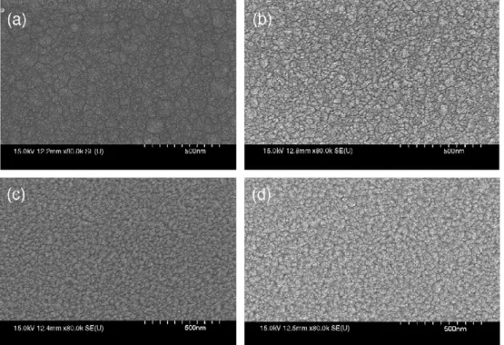
Fig. 1shows the surface images of ZnO films with various Al2O3doping concentrations. It is found that the Al2O3doping concentration has a significant influence on ZnO film surface structure. The grain size decreases as the Al2O3concentration increases. The average grain sizes of the films with Al2O3of 0 wt.%, 1 wt.%, 2 wt.% and 4 wt.% are 160, 64, 47, and 41 nm, respectively. It is indicated that Al2O3is a grain growth inhibitor in ZnO films.
Fig. 2 illustrates the XRD patterns of the ZnO films with various Al2O3doping concentrations. All of the films exhibit the preferred (002) orientation due to the minimal surface energy in the ZnO hexagonal wurtzite structure[10]. The XRD patterns also show no diffraction from randomly oriented grains or impurity phases. The intensity of the (002) peaks decreases with increasing Al2O3-doping. In addition, the location of the (002) peaks was shifted to lower 2θ angles, from 34.86° to
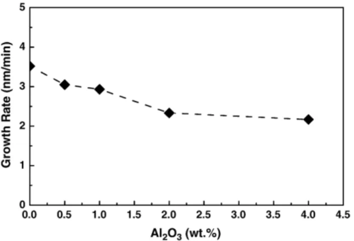
34.36° as Al2O3-doped content increases from 0 to 4 wt.%. The lattice parameter is expected to be smaller in Al2O3-doped ZnO. The effect of Al2O3concentration on the growth rate of ZnO thin films is illustrated inFig. 3. The average growth rate was calculated based on the mean value of thickness from the cross-section images of thin films. It is shown that the growth rate steadily decreases with the increase of amount of Al2O3dopant, which becomes constant at about 2.0 nm/min when the Al2O3 content is larger than 2 wt.%. For 4 wt.% Al2O3-doped film, the growth rate is observed to be lower, an approximately 0.6 times that of undoped ZnO films. The growth rate decrease with increasing Al2O3dopant suggests that ZnO growth is limited by Al2O3addition.
The dependence of the resistivity of ZnO thin films on the Al2O3doping concentration is shown inFig. 4. The resistivity decreases with an increase of Al2O3dopant in the range of 0– 4 wt.%. The electrical resistivities for pure and 4 wt.% Al2O3
-doped ZnO films are 74 Ω·cm and 2.2 × 10− 3 Ω·cm,
Fig. 1. Scanning electron micrographs of the surface of the ZnO thin films with various Al2O3-doped concentrations, (a) 0 wt.%, (b) 1 wt.%, (c) 2 wt.%, and (d) 4 wt.%.
Fig. 2. X-ray diffraction patterns of pure and Al2O3-doped ZnO thin films.
873 S.N. Bai, T.Y. Tseng / Thin Solid Films 515 (2006) 872–875
respectively. The difference of the resistivity between undoped and Al2O3 doped (4 wt.%) films is about five orders of magnitude. It is found that the resistivity decreases markedly at lower Al2O3doping concentrations and is nearly constant above 2 wt.% with a value around 2.2 × 10 −3 Ω·cm. There is no apparent change in the electrical resistivity for the ZnO films with above 2 wt.% Al2O3. The drop in resistivity is attributed to the creation of defects in ZnO films due to the Al2O3dopant. We may presume that the aluminum will replace zinc in the ZnO, which can be written as
Al2O3¼ 2AlþZnþ 3Oxoþ V2−Zn ð1Þ
Therefore, a vacancy is formed at a Zn2+site in the lattice of Al2O3doped ZnO. On the other hand, the film was deposited in Ar gas. The following defect equation may also occur
Oxo¼ 1=2O2ðgÞ þ V2þo þ 2e− ð2Þ
By adding Eqs. (1) and (2), we can get Al2O3¼ 2AlþZnþ 2Oxoþ 1=2O2ðgÞ þ 2e−
The change in the resistivity shown in Fig. 4 may be attributed to such an increase in electron concentration.
The Al2O3 doping causes ZnO films with smaller grain size and higher charge carrier density in this study. The ZnO films with higher Al2O3 doping concentration will have a higher charge carrier density. In addition, the smaller grain size caused by higher Al2O3 concentration may result in higher grain boundary scattering. It is well known that higher charge carrier density will result in lower resistivity; however, higher grain boundary scattering will cause higher resistivity. According to the resistivity measurement results, we can reasonably infer that the decrease of resistivity of the ZnO films is mainly due to the increase of charge carrier density.
Fig. 5 shows the optical transmittance spectra of ZnO thin films with various Al2O3doping concentrations. As shown in
Fig. 5, the ZnO films have a high average transmittance of approximately 85% in the wavelength range 200–800 nm with oscillatory character due to interference effects[11]. The average transmittance of the ZnO films is increased by Al2O3 doping. The higher the Al2O3dopant concentration, the more transparent the films become. Based on the SEM and XRD experimental results, the thickness of the ZnO films decreases as the content of Al2O3dopant is increased. The thickness of the ZnO films with Al2O3 of 0 wt.%, 0.5 wt.%, 1.0 wt.%, 2.0 wt.% and 4.0 wt.% is 211, 183, 176, 140, and 130 nm, respectively.
It is found that ZnO films have sharp ultraviolet absorption characteristics in the transmittance spectra. The absorption edge is observed in the wavelength range of 300–400 nm for the films investigated. The absorption edge shifts toward higher energy sides for the ZnO films formed at higher Al2O3 doping levels. According to the position of the absorption edge, the energy gap of the ZnO films is evaluated as about 3.4 eV. The evaluation of the energy gap from absorption edge position assumes that the ZnO films have a direct transition. What is more notable is that the various thicker layers with interference follow the “envelope” of the doped films, indicating that none of the films show absorption down to about 370 nm and a “shoulder” on the curve develops, showing increase in optical bandgap most likely due to the Burstein-Moss effect[12].
Fig. 5. Optical transmittance spectra of ZnO thin films with various Al2O3-doped
concentrations indicated.
Fig. 4. Variations of the resistivity of ZnO thin films with Al2O3-doped
concentration.
Fig. 3. Variations of the growth rate of ZnO thin films with Al2O3-doped
concentration.
4. Conclusions
Highly transparent conductive ZnO thin films with various Al2O3doping concentrations were produced on 1737F Corning glass substrates by R.F. magnetron sputtering. These ZnO films have a highly (002) preferred crystal orientation. The grain size of ZnO thin films decreases as the Al2O3content is increased in the doping range of 0–4 wt.%. The electrical resistivity significantly decreases from 74Ω·cm for pure ZnO to 2.2×10− 3Ω·cm for 4 wt.% Al2O3-doped ZnO films. The charged carrier density has larger effect on the resistivity of Al2O3-doped ZnO films in comparison to grain size. Optical transmittance measurement shows that an average transmittance above 85% in the visible range is obtained for ZnO films deposited at different Al2O3 doped concentrations. The average transmittance increases when the Al2O3dopant increases. The ultraviolet absorption edge is also observed in the wavelength range of 300–400 nm for all the ZnO films. These sharp absorption edges correspond to the energy gap of around 3.4 eV with the assumption of the direct transition.
Acknowledgements
The authors gratefully appreciate the financial support from the National Science Council of Republic of China under Project
No. NSC 93-2216-E009-024. Mr. F. C. Chuang is thanked for his help in experimental works.
References
[1] X. Jiang, F.L. Wong, M.K. Fung, S.T. Lee, Appl. Phys. Lett. 83 (2003) 1875.
[2] J. Yoo, J. Lee, S. Kim, K. Yoon, I.J. Park, S.K. Dhungel, B. Karunagaran, D. Mangalaraj, J. Yi, Thin Solid Films 480 (2005) 213.
[3] M. Bender, E. Gagaoudakis, E. Douloufakis, E. Natsakou, N. Katsarakis, V. Cimalla, G. Kiriakidis, E. Fortunato, P. Nunes, A. Marques, R. Martins, Thin Solid Films 418 (2002) 45.
[4] N.R. Aghamalyan, E.A. Kafadaryan, R.K. Hovsepyan, S.I. Petrosyan, Semicond. Sci. Technol. 20 (2005) 80.
[5] S.N. Bai, T.Y. Tseng, J. Appl. Phys. 74 (1993) 695.
[6] E.G. Fu, D.M. Zhuang, G. Zhang, W.F. Yang, M. Zhao, Appl. Surf. Sci. 217 (2003) 88.
[7] V. Srikant, D.R. Clarke, J. Appl. Phys. 81 (1997) 6357. [8] V. Gupta, A. Mansingh, J. Appl. Phys. 80 (1996) 1063. [9] Y. Igasaki, H. Saito, J. Appl. Phys. 70 (1991) 3613.
[10] J.F. Chang, H.L. Wang, M.H. Hon, J. Cryst. Growth 211 (2000) 93. [11] H. Nanto, T. Minami, S. Shooji, S. Takata, J. Appl. Phys. 55 (1984) 1029. [12] Z.B. Fang, Y.S. Tan, H.X. Gong, C.M. Zhen, Z.W. He, Y.Y. Wang, Mater.
Lett. 59 (2005) 2611.
875 S.N. Bai, T.Y. Tseng / Thin Solid Films 515 (2006) 872–875