國立交通大學
電子工程學系電子研究所碩士班
電子工程學系電子研究所碩士班
電子工程學系電子研究所碩士班
電子工程學系電子研究所碩士班
碩士論文
碩士論文
碩士論文
碩士論文
III
III
III
III-
-
-
-V
V
V 族多接面太陽電池表面光柵
V
族多接面太陽電池表面光柵收光
族多接面太陽電池表面光柵
族多接面太陽電池表面光柵
收光
收光
收光增益的
增益的
增益的
增益的研究
研究
研究
研究
The Study of Photon Absorption Enhancement by Surface-Relief
Grating on III-V Multi-Junction Solar Cell
研究生
研究生
研究生
研究生:
:
: 史宜靜
:
史宜靜
史宜靜
史宜靜
指導教授
指導教授
指導教授
指導教授:
:
:
: 林聖迪
林聖迪
林聖迪
林聖迪
博士
博士
博士
博士
中華民國九十九年九
中華民國九十九年九
中華民國九十九年九
中華民國九十九年九月
月
月
月
III
III
III
III-
-
-
-V
V
V 族多接面太陽電池表面光柵收光增益的研究
V
族多接面太陽電池表面光柵收光增益的研究
族多接面太陽電池表面光柵收光增益的研究
族多接面太陽電池表面光柵收光增益的研究
The Study of Photon Absorpti
The Study of Photon Absorpti
The Study of Photon Absorpti
The Study of Photon Absorption Enhancement by Surface
on Enhancement by Surface
on Enhancement by Surface-
on Enhancement by Surface
-
-
-Relief
Relief
Relief
Relief
Grating on III
Grating on III
Grating on III
Grating on III-
-
-V Multi
-
V Multi
V Multi-
V Multi
-
-
-Junction Solar Cell
Junction Solar Cell
Junction Solar Cell
Junction Solar Cell
研
研
研
研
究
究
究
究
生
生
生
生
:
:
:
:
史宜靜
史宜靜
史宜靜
史宜靜
Student:
Student:
Student:
Student:
Yi
Yi
Yi
Yi-
-
-
-Ching,Shih
Ching,Shih
Ching,Shih
Ching,Shih
指導教授
指導教授
指導教授
指導教授:
:
:
:
林聖迪
林聖迪
林聖迪
林聖迪
Advisor:
Advisor:
Advisor:
Advisor:
Sheng
Sheng
Sheng
Sheng-
-
-Di, Lin
-
Di, Lin
Di, Lin
Di, Lin
國
國
國
國
立
立
立
立
交
交
交
交
通
通
通
通
大
大
大
大
學
學
學
學
電子工程學系電子研究所碩士班
電子工程學系電子研究所碩士班
電子工程學系電子研究所碩士班
電子工程學系電子研究所碩士班
碩士論文
碩士論文
碩士論文
碩士論文
A Thesis A Thesis A Thesis A ThesisSubmitted to Department of Electronic Engineering and Submitted to Department of Electronic Engineering and Submitted to Department of Electronic Engineering and Submitted to Department of Electronic Engineering and
Institut InstitutInstitut
Institute of Electronics e of Electronics e of Electronics e of Electronics
College of Electrical and Computer Engineering College of Electrical and Computer Engineering College of Electrical and Computer Engineering College of Electrical and Computer Engineering
National Chiao Tung University National Chiao Tung University National Chiao Tung University National Chiao Tung University
in partial Fulfillment of the Requirements in partial Fulfillment of the Requirements in partial Fulfillment of the Requirements in partial Fulfillment of the Requirements
for the Degree of for the Degree of for the Degree of for the Degree of
Master in Electric Engineering Master in Electric Engineering Master in Electric Engineering Master in Electric Engineering
Sep SepSep
Sep 2010 2010 2010 2010
Hsinchu, Taiwan, Republic of China Hsinchu, Taiwan, Republic of China Hsinchu, Taiwan, Republic of China Hsinchu, Taiwan, Republic of China
中華民國九十九年九
中華民國九十九年九
中華民國九十九年九
III
III
III
III-
-
-V
-
V
V 族多
V
族多
族多接面太陽電池表面
族多
接面太陽電池表面光柵
接面太陽電池表面
接面太陽電池表面
光柵
光柵收光增益的
光柵
收光增益的
收光增益的
收光增益的研究
研究
研究
研究
學生: 史宜靜 指導教授: 林聖迪
國立交通大學
電子工程學系 電子研究所碩士班
摘要 摘要摘要 摘要 本論文主要在於研究如何在 III-V 族太陽能電池表面製作光柵以增廣可 利用的太陽光譜頻寬與大角度的吸收。首先我們利用一套嚴格耦合波的數學 方法來設計在 AM1.5 下太陽光譜的最佳光柵結構,接著利用電子微影技術將 光柵生長在 InGaP/GaAs/Ge III-V 族太陽電池表面;最後進行變角度量測。 量測結果發現,擁有光柵的太陽能電池普遍擁有較高轉換效率,尤其在大 角度上的表現,與理論預測的趨勢大致相同。雖然光的吸收率與能量轉換效 率並沒有直接關係,但至少我們可以證實擁有光柵的太陽電池卻實在整體效 率與大角度的吸收都比只生長抗反射層的電池來得高。故此,如果我們能夠 利用低成本的方式大量複製此光柵在太陽能電池上,對於光跡追蹤與其他地 面發電運用都有一定的貢獻。The Study of Photon Absorption Enhancement by
Surface-Relief
Grating on III-V Multi-Junction Solar Cell
Student: Yi-Ching Shih Advisor: Dr. Sheng-Di Lin
Department of Electronics Engineering & Institute of Electronics National Chiao Tung University
Abstract
In this dissert, we want to study the improvement of light trapping mechanism due to grating grown its surface in order to achieve higher efficiency at higher incidence. Firstly, we adopt a numerically stable mathematical calculation called rigorous coupled-wave analysis, RCWA, to optimize the profile of grating structure. Then we realize it onto real InGaP/GaAs/Ge III-V MJ solar cell. Lastly, the efficiencies will be measured under standard AM1.5G solar spectrum at various incidences.
In general, the experiment results of samples with grating present higher efficiency than those without. Better performance can also be achieved at larger oblique incidence. Surprisingly, the efficiencies follow the trend of transmittance rate as RCWA has estimated. Although it is quite complicated to judge the relation categorically; we can still attribute the improvements of increasing photon penetrating to grating mechanisms. As a result, if we can find another more effective and less costly way during fabrication process, the contribution of this light trapping structure could be widely extended due to the light tracking system and terrestrial applications have become more prosperous in recent years.
Acknowledgement (致謝
致謝
致謝
致謝)
回想過去研究的日子,覺得自己何其幸運可以從電物跳到電子所殿堂,然 後又是何其幸運進入 MBELab 這大家庭,尤其豐富的資源與周全的設備,讓我 研究生涯不用為了排隊等儀器,聽著鳥叫做實驗。我首先要非常感謝我的指 導教授 林聖迪博士,當初肯接納我,並選擇讓我嘗試自己的興趣,研究實驗 室並不熟悉的領域;最後一年還答應讓我當交換學生去德國開闊視野。雖然 我的研究可能不盡理想,但在這懵懂摸索的過程卻收穫滿滿;更加的了解自 己、了解做學問的態度、學會獨立思考的價值。也謝謝老師爽朗的胸襟,包 容我這有點極端神經質的個性。再來,感謝實驗室大家長 李建平博士,老師 的真知灼見常常一針見血的點出我的缺點,嚴師益友的個性,一直是我的表 率;謝謝老師常常不吝讚美,讓我更有信心往前走。 還有幫我很多忙的 羅明城學長 凌鴻緒學長 張家華學長 傅英哲學長 潘 建宏學長 鄭旭傑學長還有小孟學妹…;一起奮鬥,一起玩耍的憨憨們:賴大 師、小豪、歪哥、仁哥、KB、皓皓、小微、阿公、Queena…以後也要一直玩 下去唷!還有貼心的柏存、鄭濬。在此也特別感謝許裕彬學長,因為你的鼓 勵,讓我撐過很多熬夜的夜晚;祝福你在美國找到自己的一片天,學成歸國。 最後要感謝的就是我的父母,我的家人;一路走來都很支持我做的每項決 定,讓我能一無反顧的往前走,還要時常容忍我一觸及發的壞脾氣。能拿到 這學位不是偶然,而是建構在很多很多人無私幫忙與鼓勵,在此獻上由衷的 感謝,希望大家未來都能快樂健康,並找到自己的興趣勇往直前!Contents
Chinese Abstract (中文摘要中文摘要中文摘要) ---中文摘要i
English Abstract (英文摘要英文摘要英文摘要英文摘要)---ii
Acknowledge (致謝致謝致謝致謝)---iii
Contents (目錄目錄目錄)---目錄iv
Figure List (圖表清單圖表清單圖表清單)---圖表清單v
Chapter 1 Introduction ---1
1.1Basic Principle of Solar Cell
---1.2Efficiency
---1.3Multi-junction Solar Cells
---1.4Minimizing
Reflection---2
6
11
14
Chapter 2 Rigorous Couple-Wave Theoretical Formulism andCoding16
2.1Basic Concept of
RCWA---2.2Formulism in Computational Algorithm
---16
24
Chapter 3 Simulation Results and Analysis ---26
3.1 Anti-Reflection
Coating---3.2 Sub-Wavelength Grating
Structure---3.3 Broadband Characteristic at Oblique
Incidence---26
28
36
Chapter 4 Experimental Analysis and Discussion---39
4.1 Sample Design and Fabrication
Process---4.2 Measurement and
Analysis---4.3
Discussion---39
46
58
Chapter 5 Conclusion---61
Reference---62
Appendix---64
Figure Catalog
Chapter 1Figure 1.1 The circuit of pn junction solar cell with external load 3
Figure 1.2 Schematic photon-generated carrier process 4
Figure 1.3 Equivalent circuit with parasitic series Rs and shunt Rsh resistance 4
Figure 1.4 Definition of air mass 5
Figure 1.5 ASTM standard of solar spectrum irradiation AM1.5 5
Figure 1.6 The current voltage and power output diagram of solar cell 9
Figure 1.7 Detailed balanced limit of solar efficiency 9
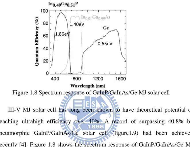
Figure 1.8 Spectrum response of GaInP/GaInAs/Ge MJ solar cell 11
Figure 1.9 Schematic GaInP/GaInAs/Ge structure and equivalent circuit 13
Figure 1.10 Band diagram of GaInP/GaInAs/Ge solar cell 13
Figure 1.11 The cross section SEM image of graded-index coating 14
Figure 1.12 Spherical particles of omnidirectional AR coating 15
Figure 1.13 The cross section SEM image of 1D rectangular grating 15
Chapter 2
Figure 2.1 Schematic interpretation of grating principle 16
Figure 2.2 Floquent equation in wave vector space 17
Figure 2.3 Schematic diagram of grating structure 18
Figure 2.4 TE diffraction within 1D grating structure unit cell 20
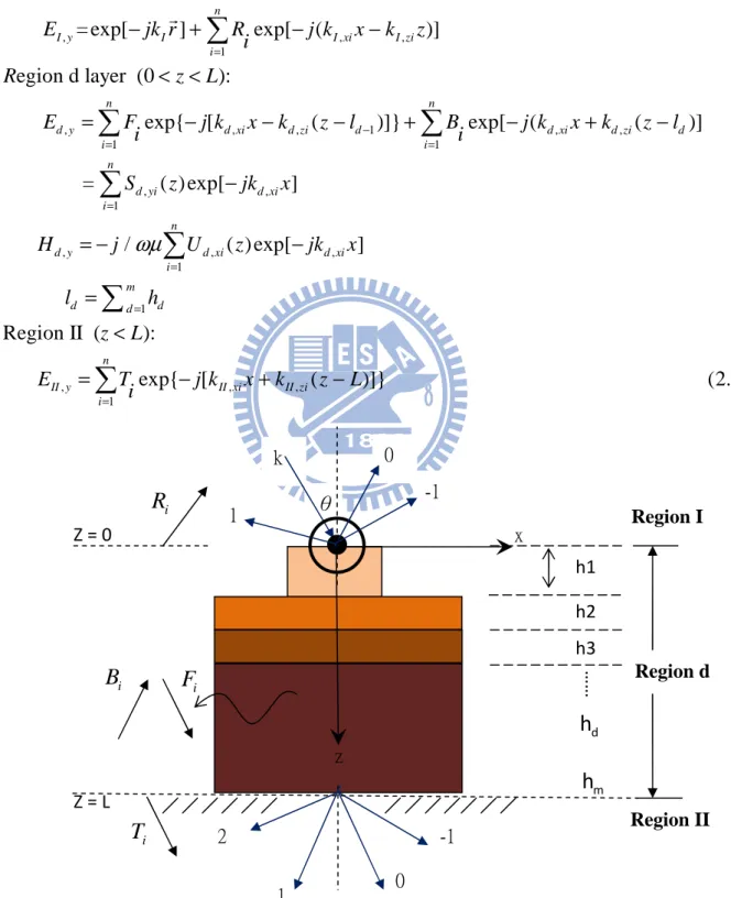
Tablee 2.1 Summary of full mathematic formulation for RCWA 23
Tablee 2.2 Summary of partial mathematic formulation for RCWA 24
Tablee 2.3 Computational algorithm diagram 25
Chapter 3
Figure 3.1 Contour map of transmittance under standard solar spectrum as functions of SiO2andSi N3 4thickness
26
Figure 3.2 The comparison of surface transmittance with and without AR to normalized black body power density at 6000K
27
Figure 3.3 The transmittance comparison of TSolar to wavelength 600 nm as function of grating depth, with period 0.4 um, filling factor 0.3
28
Figure 3.4 Contour map of transmittance under standard solar spectrum of grating period 0.35um as functions of height and FF
33
Figure 3.5 The optimum value of grating profile 34
Figure 3.6 The unit cell of optimum periodic 1D grating profile 34 Figure 3.7 Transmittance comparison of sample with AR and grating as function
of wavelength
35
Figure 3.8 TSolar Comparison of AR and Grating as function of incident angle 35 Figure 3.9 The TSoalr difference between sample with and without grating 36 Figure 3.10 The contribution of TE & TM modes to TSolar as function of 36
incident angle
Figure 3.11 Contour map of transmittance under standard solar spectrum as
functions of SiO2andSi N3 4thickness
37
Figure 3.12 Displays of the transmittance diffractive order distributions as function of incident angle in TM(left) and TM(right) polarization
38
Tablee 3.1 Contour map of reflectivity of different grating H as functions of period and filling factor for the standard solar spectrum
30
Chapter 4
Figure 4.1 Structure of VPEC’S triple junction concentration solar cell 39
Figure 4.2 Photo lithography process for electrode pattern 42
Figure 4.3 Electrode contact configuration 42
Figure 4.4 Anti-reflection coating process 43
Figure 4.5 Electrode contact configuration after removing AR by using acid BOE
43
Figure 4.6 Figure 4.6 E-Beam lithography process for sub-wavelength grating 44 Figure 4.7 Top view of SEM image of grating with period 350nm, depth100nm
and width 100nm under (a) large scale (b) small scale
45
Figure 4.8 Solar simulator system diagram 46
Figure 4.9 I-V curves of (a) dark current with sample A_AR and A_1t (b) under illumination with sample A_AR, A_1 and W/O AR.
47
Figure 4.10 Simulation I-V curve of III-V solar cell done by APSYS commercial software which assumes front ARC layers to be MgF /ZnS2
49
Figure 4.11 External quantum efficiency, EQE, of each subcell 51
Figure 4.12 Ratio of short circuit current density between sample A_1 and A_AR over incident angle
52
Figure 4.13 Ratio of number of photons utilized by surface of grating over ARC 52
Figure 4.14 Self-decay ration between sample A_1 and A_AR 54
Figure 4.15 Measured efficiency difference between A_1 and A_AR along different incident angle
54
Figure 4.16 Tsolar as function of filling factor at normal incidence 55 Figure 4.17 Measured efficiency differences along different incident angle of (a)
device B and (b) device C.
56
Figure 4.18 Simulation of TSolar differences for different filling factor along different incident angle
57
Figure 4.19 The transmittance comparison of wavelength distribution of surface with (a) grating structure on AR (b) AR at increasing angle of incidence, along the arrow.
58
Chapter 1
Introduction
Solar energy absorbed by land and oceans on Earth is over 3.85 10 J× 24 in one year. Comparing with the approximate amount of energy 4.87 10 J× 20
human needed in a year, it is assumed to be the most renewable green energy in the aspect of environmental protection and has aroused many attentions during crisis of energy shortage in recent years. Many researches have been aiming at finding more sufficient and costless ways to effectively utilize this broadly distributed solar spectrum. III-V multi-junction (MJ) solar cell has long been known for its high conversion efficiencies for its absorption regions can be separated into several subcell among different span of wavelength. Within each subcell, light and be absorbed more effectively without wasting too much photon energy as thermal dissipation than single junction do. Also its efficiency beyond the Shockley-Queisser theoretical limit for single band gap has been achieved. In addition, III-V materials not only obtain direct band gap and high absorption coefficient which shorten the absorption length, it also has the suitable band gap energy which is close to optimum according to theoretical estimation [1].
The dramatic reduction of fabrication cost due to the advancing development technologies makes III-V MJ solar cells attract more attention on both spatial and terrestrial applications. Research studies have been done on either improving lattice disorder and current mismatch on metamorphic material [2-4] or increasing photon flux density within solar cell [5-8]. Many of them have successfully enhanced efficiency by putting textured periodic structure or
roughing the surface in the way to optimize the utilization of trapped light. With most of the works had been done on Si based wafer, seldom of researches can be found onto III-V compound solar cell. Therefore, we are interested in investigating surface mechanisms on III-V MJ solar cells. This mechanism has demonstrated to have broadband and oblique anti-reflection characteristics called sub-wavelength surface relief gratings [9-11] by using numerically stable mathematical approach called Rigorous Couple-Wave Analysis (RCWA) which can be applied to solve the surface-relief and multi-layer grating structures [12-15]. In the following chapter we apply RCWA as a tool to optimize the profile of surface relief gratings and realize it by using dielectric materials
2 3 4
SiO and Si N onto actual GaAs/InGaP/Ge III-V MJ solar cell.
1.1
Basic Principle of Solar Cell
I-V characteristicSolar cell is a pn junction semiconductor with zero bias applied externally and can deliver electrical power when the generation of electron-hole pairs inside depletion region is swept by internal electric field (figure 1.1). The absorption of photons with energy larger than threshold, the band gapEg, creates electron-hole pairs and generates the output reverse-bias currentIL. Figure 1.2 is the schematic photon-generated carrier process inside depletion region. It then produces a forward bias V back onto the cell when passing through the load in which induces the ideal diode current,Id, following the ideal diode equation in forward-bias direction. The total photovoltaic current is referred to as: [16]
0[exp( ) 1] (1.1) L d d I I I eV I I kT = − = −
The parameter I0 is defined as ideal reverse saturation bias current.
Figure 1.3 shows the equivalent one diode model circuit inside semiconductor when taking parasitic the series resistance,Rs,and shunt resistance,Rsh, into consideration [17].The characteristic of ideal diode equation with two resistances can be represented:
0 ( ) {exp[ ] 1} (1.2) s s sh V IR q V IR I I R kT − − = + − s
R accounts for the ohmic losses due to metallic contact is usually assumed to be zero in ideal case and Rsh relates to the current leakages by defects during process or interconnection is regarded as infinity. By studying the electrical
- - + + - - + + - - + + P
I
L N+ V -
I
dI
hvR
shR
SD
+
V
D-
+
V
-
I
Figure 1.3 Equivalent circuit with parasitic series Rs and shunt Rsh resistance
1. 2. 3.
E
g e- h+I
LFigure 1.2 Photon-generated carrier process
properties allows us to extract more detail parameters of solar cells. Some reports even suggest two-diode model circuit is more suitable in describing the behavior its performance [18,19] which is beyond the scope of our discussion.
Standard test condition
The attenuation of solar spectrum by scattering and absorption of atmosphere is qualified by so called “Air Mass” defined as figure 1.4:
1 AirMass
cos
θ
s= (1.3)
The standard test condition (STC) for solar cells is the Air Mass 1.5G spectrum (figure 1.5) designed for flat plate modules. It is a standard terrestrial solar spectrum irradiance distribution developed by American Society for Testing Materials (ASTM) modeled by a sun-facing collector tilt 370 from horizon and
the relative light path to the direct solar beam is 1.5 times longer, corresponding to solar zenith angle at 48.19∘. The integrated power density is normalized as
s
θ
Figure 1.4 Definition of air mass
AM 1.5 48.19∘ Atmosphere Earth Zenith 1000W m/ 2 at the temperature25oC.
Figure 1.5 ASTM standard of AM 1.5G solar spectrum
irradiation AM1. 0 500 1000 1500 2000 2500 3000 0.0 0.5 1.0 1.5 Wavelength HnmL S p ec tr al Ir ra d ia ti o n W H m -2 n m -1 L ASTM G170-03 Global tilt
1.2
Efficiency
Definition of efficiencyMany papers have discussed about how to improve the efficiency of solar cells based on the basic rule of theoretical calculation, called detailed balance limit. According to W. Shockley and H. J. Queisser [1], if we consider only the ultimate efficiency, Qu , that each photon with energy greater than band gap,Eg(hνg), will contribute one electron without any losing mechanisms. The maximum efficiency can be obtained as the ratio of power delivered by the cell over the solar power impinging onto surface area A.
u p g s N E A Q AP = (1.4) 1 2 2 1 3 2
number of photon with energy greater than E 2
[exp( ) 1]
Solar energy density falling upon device 2 [exp( ) 1] g g p g s s s N h d c kT P h h d c kT ν ν π ν ν ν π ν ν ν ∞ − ∞ − = = − = = −
∫
∫
In real case we have to take other mechanisms, radiation and nonradiation generation or recombination, into account which may generally diminish Qu. In order to improve the efficiency of solar cell, it is necessary to find out the physical function inside each device, thus suggesting possible improvements.
When pn junction solar cell is subjected to radiation, it then produces the photocurrent,IL in the reverse-bias direction where the ideal diode equation becomes: 0[exp( ) 1] (1.5) L eV I I I kT = − −
in which the symbol I0 representing reverse saturation current is resulted from
the generation of hole-electron pair due to ambient blackbody temperature T and its own, either nonradiation,Gnr, or radiation,Gr, process. These processes are theoretically independent of external bias. kT
e can be rewritten as a voltage,Vc,
which is generated by the temperature itself. ILis also referred to as the short-circuit current, Ish, whenever the external bias tends to be zero which is basically generated under illumination,eGs, and the recombination loss in the access of blackbody radiation from the cell, eRc, is also taken into account.
0 ( ) ( ) r nr L s c I e G G I e G R = + = − (1.6)
Another term of most interest for solar cell is open voltage,Voc which can be obtained by setting I in (1.5) to zero, thus we can obtain.
0 ln(1 L) oc c I V V I = + (1.7)
According to theory, the maximum open-voltage can be derived as the band gap voltage Vg as the temperature of the cell approaches zero (1.8). This is resulted from a photon producing an electronic charge with energyEgcan contribute the specific potential energy. Also under this circumstance, no excess generation or recombination process will take place.
0
lim oc g
T→ V =V (1.8)
efficiency, we can derive the upper limit of efficiencyη. Conversion efficiency in general is defined as the ratio of maximum power that a cell can deliver to a matched load over total incident power, Ps, from the sun.
. m m sh oc s s I V I V FF P P η = = (1.9)
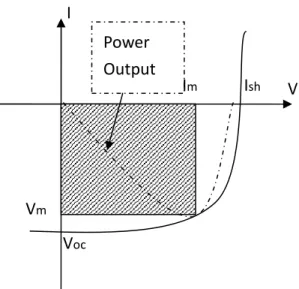
It is shown in figure 1.6 where Im and Vm is the current density and voltage of maximum output power. Filling factor, FF, defined as I Vm m /I Vsh oc is also a key
measurement of solar cell performance and typically is around 0.7~0.8.
Improvement of efficiency
Detail balanced limit requires the following assumptions: (1)The probability, f , of a photon with energy greater thanEg that will produce a hole-electron pair must be unity;(2) Only radiative recombination mechanism is required;(3) The charges are completely separated and transported to external circuit without loss. Figure 1.7 shows the theoretical efficiency calculated with cell and sun temperatures at 300K and 6000K respectively [1]. Curve f assumes all the assumption above to be ideal and the incident angle subtended by the sun upon solar cell to be normal. Other curves decrease gradually from curve g to i. as f less than unity or larger the incident angle. This indicates the maximum efficiency is approximately 31% which corresponds to an energy gap value around 1.3~1.4eV.
Equation (1.9) can be redefined in terms of ultimate efficiency (1.4) as below: . . . oc u g V Q FF f V η = (1.10)
Actual device do not obey the ideal relationship curves in figure 1.7. The reasons for these deviations come from the last three terms in equation (1.10). Many researches have been studied and published to deal with these questions
I V Voc Ish Im Vm Power Output
Figure 1.6 The current voltage and power output diagram of solar cell
and some methods based on the basic physical concept can be done by focusing on the assumptions presumed:
(1) Only single junction is concerned. This can be solved by increasing the number of band gap such as to parcel out the preferable wavelength into each subcell corresponding to different band gaps. Multi-junction (multi-band) solar cells have the potential of achieving high efficiency over 53.6% theoretically
(2) Photon flux density depends only on the temperature of sun and the angle of light subjecting on cell. The concentration light increases the geometrical factor,Fs, and widens the angular range from θs to θc subtended by sun, thus enhancing the total flux intensity by S [17].
2 2 sin sin c s S θ θ = (1.11)
(3) Increase the number of electron-hole pair that each photon can create. This requires the mechanism called impact ionization.
(4) Some fraction of incident light will be reflected from the surface of cell,R, and others will pass inside but attenuate exponentially along the way. Unless there is any chance to diminish the reflection from the surface toward zero and absorb each incident photon perfectly, the probability of gaining one electron-hole pair per photon, f , would never approach unity and the
equation (1.10) would never attain ultimate target. Therefore, the following equation about f should be considered.
(1 )(1 x)
f = −R −e−α (1.12)
α
isthe absorption coefficient of the cell. If theα
is large, the photons areabsorbed over a relatively short distance.
(5) Another problem has not been considered is about how to harness the excess kinetic energy of the photo-generated carriers over band gap before they dissipate into thermal energy which increases the possibilities of other non-radiation recombination, Auger recombination for instance. The idea of hot carrier solar cell then comes up with the solution to recycle this excess energy but the effect is still under investigation [20].
Practical methods are still being done with regard to enhancing the presumptive analysis toward ideal expectation. The first two strategies are more commonly used in the III-V multi-junction solar cells (figure 1.9) and further discussion about (4) is in section, 1.4.
1.3 Multi-junction Solar Cells
Detail balanced theory estimates the upper limit of single junction where only a narrow range of specific wavelength can be absorbed. On the contrary, multi-junction (MJ) solar cells consisting of multiple subcells with different bandgaps can efficiently convert broadband of photon energy in to photocurrent so their efficiency can beat up cells with single junction.
In 1990, Fraas group invented a two junction mechanically stacked AlGaAs/ GaAs solar cell and achieved over 35% efficiency [21]. But this kind of devices though was estimated to have higher conversion efficiency due to fewer defects between the connections of two subcells, it requires individual circuit for each subcell, which makes the processing more complicated. Therefore, over the pass few decades, there have been great improvements for monolithic cascaded junction solar cell [22,23]. The achievements of low-loss tunnel junction between two or more interconnection of cells and the largely reduced lattice or
1.86eV V
1.40eV
0.65eV
Figure 1.8 Spectrum response of GaInP/GaInAs/Ge MJ solar cell
current mismatch make monolithic cascaded solar cell more realistic and popular in recent years.
III-V MJ solar cell has long been known to have theoretical potential of reaching ultrahigh efficiency over 40%. A record of surpassing 40.8% by metamorphic GaInP/GaInAs/Ge solar cell (figure1.9) had been achieved recently [4]. Figure 1.8 shows the spectrum response of GaInP/GaInAs/Ge MJ solar cell and the schematic cell structure with its equivalent model circuit in is shown in figure 1.9. Obviously, it divides solar spectrum into three parts which nearly covers the main energy distribution. The development of optically and electrically low-loss tunnel junction is realized and the band diagram can be schematically shown in figure 1.10 [3]. Higher photon energy is mainly extracted by InGaP top subcell, medium energy by GaAs in the middle and lowest energy by Ge at the bottom. Where we can notice the formation of thin and wide-band-gap tunnel junction is a crucial issue to realize high-efficiency MJ solar cells. Although MJ solar cells are mostly used for space application, the investigations for its terrestrial applications have begun to attract more
attentions in recent years.
Figure 1.9 Schematic GaInP/GaInAs/Ge structure, right, and equivalent circuit, left.
Figure 1.10 Band diagram of GaInP/GaInAs/Ge solar cell Tunnel Junction
1.4 Minimizing Reflection
In order to maximize the optical absorption in achieving high performance solar cells, many solutions have been demonstrated about how to diminish the reflection on the surface over extensive spectrum range. Various anti-reflection coatings (AR) are widely utilized by growing a thin film of dielectric layer on the front of surface but that can only reduce the reflectivity at certain specific wavelength and are also restricted on narrow angle of incidence.
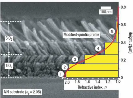
In 1880, Lord Rayleigh first mathematically calculated the “graded refractive index layer” contain broadband anti-reflection characteristic and, in 2007, Martin’s group had reported that an oblique-angle deposition of TiO2
and SiO2 coating [6] (figure 1.11) has low reflectivity over the entire visible
and near infrared spectrum. At the same time, another group demonstrated a new microscale surface texturing on solar cell in the shape of spherical (figure 1.13) and proposed to be an omni-directional anti-reflection coating [5] accompanying mathematical calculation called rigorous coupled wave analysis (RCWA).
However, different attempts have been studied for the structures of AR over broadband spectrum, sub-wavelength surface-relief grating (figure 1.12) has also been long investigated to have such broadband absorption characteristic [9,24,25]. At larger propagation angles, most of the light is coupled into higher transmitted diffraction order which enhance the absorption length and extensively increase the generation of electron-hole pairs. Although the advantage of sub-wavelength grating is proposed, it still has not yet been fabricated on the ultrahigh efficiency III-V triple junction solar cells.
Before the grating structure experimentally make on a real III-V triple junction solar cell, the numerical mathematics RCWA will be briefly discussed and treated as a numerical analysis approach during the whole optimum and ideal simulations in the following chapter.
Figure 1.12 Spherical particles of omnidirectional ARC
Chapter 2
Rigorous Couple-Wave Analysis Theory and Coding
2.1 Basic Concept of RCWA
Grating equationThe principle of constructive interference only exists when the light scattered in phase which means the path difference equals the multiple of wavelength. The concept can be visualized in figure 2.1 and expressed in a simple equation (2.1), called the grating equation.
sin
θ
m sinθ
i mλ
m 0, 1, 2....Λ − Λ = = ± ± (2.1) m number the order of diffractive wave. This can transform into another more general form in terms of wavevector, k, in the direction of x, called Floquent condition: 2 mx Ix k = k +mK K =
π
Λ (2.2) Λ represents the grating period, kIx and kmx are the x component of m orderm θ sinθi Λ i θ sinθm Λ Λ I i
Figure 2.1 Schematic interpretation of grating principle incidence diffraction
x y
i
1
-1
-2
-3
Ixk
k
mx K + 3K −k
IReflection
Transmission
2K − −KRegion I
Region i
I n i n0
Figure 2.2 Floquent equation in wavevector space
wavevector in incident region I and transmission region. K can be called grating
vector. Figure 2.2 shows the schematic Floquent condition (2,2) between two
media in vector space. The radius is the amplitude of propagating wavevector.
Only a limited number order of wave can exist depending on the subtraction and
addition of grating vector.
Sub-wavelength surface relief grating is a kind of diffraction structure in the
scale of wavelength that mostly produce zero order and all higher order
propagate as evanescent wave. In 1D grating, it sets the maximum limit on the
maximum grating period as
λ
0 being the vacuum wavelength [9]:0 sin I i i n n
λ
θ
Λ ≤ + (2.3)RCWA formulism
RCWA is one of the numerical solutions being widely applied and
studied in the interest of dealing with diffractive characteristics of
electromagnetic waves on dielectric gratings. It expands the resolution wave in
the form of plane wave components, and the amplitude of each component are
obtained by matching the boundary conditions between two refractive materials.
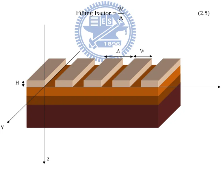
In the general case of one-dimensional rectangular grating (figure 2.3), the
grating vector is parallel to x direction and filling factor is defined as the ratio of
width of rectangular over period.
Filling Factor= W Λ (2.5) X y z Λ W H
For the case of planar diffraction solution, electromagnetic wave can be
easier to deal with by decomposing into TE and TM polarization, where
electric and magnetic field are normal to the plane of incidence (x-z plane)
respectively. TE and TM wave can be handled individually. Here we briefly
present the formulation of TE polarization. The extension of TM problem is
straightforward, thus it is not mentioned below.
TE component
Sub-wavelength gratings has been theoretically proved to obtain the
homogeneous properties [10, 24], thus Maxwell’s equation can be described in
the form of (2.6), with electromagnetic boundary conditions as (2.7) [27] Maxwell's equation in linear and homogeneous media
( ) ( )
(2.6)
( ) 0 ( )
Accompany with the Boundary Condition below
( ) ( ) 0 // // ( ) f B i E iii E t E ii B iv H J f t I II I II i E E iii E E I II ii B B ρ ε ε σ ε ∂ ∇ ⋅ = ∇ × = − ∂ ∂ ∇ ⋅ = ∇ × = + ∂ − = − = ⊥ ⊥ − = ⊥ ⊥ ur ˆ 0 ( ) (2.7) // // I II iv H H K n f − = ×
Where ˆn is unit vector with the direction normal to grating surface.
ρ
is the free charge,σ
f the surface free charge density,Kf the surface free current andJf the free volume current density. Those values mentioned above indielectric materials are generally treated as zero.
ε
is the relative permittivity. (2.6) satisfies the Maxwell’s equation in differential form:y y x z x z y E E H H j H j H j E z µω x µω z εω x ∂ = ∂ = ∂ = + ∂ ∂ ∂ ∂ ∂ (2.8)
…… h3 h2 h1 1 x 1 k 0 -1 θ z 0 -1 2
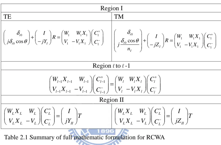
Figure 2.4 TE diffraction within 1D grating structure unit cell
i B i T Z = 0 Z = L d h i F i R Region d Region I Region II m h
As for TE polarization, incident electric field Ey in y direction is expanded into summation of total diffractive waves from region I to II which are schematically shown within the unit cell of periodic structure in figure 2.4.
, , , 1 , , , 1 , , 1 1 , , 1 , Region I ( 0): = exp[ ] exp[ ( )] egion d layer (0 ): exp{ [ ( )]} exp[ ( ( )] = ( ) exp[ ] / n I y I I xi I zi i n n d y d xi d zi d d xi d zi d i i n d yi d xi i d y d z E jk r R j k x k z i R z L E F j k x k z l B j k x k z l i i S z jk x H j ωµ U = − = = = > − + − − < < = − − − + − + − − = −
∑
∑
∑
∑
r , , 1 1 , , , 1 ( ) exp[ ] Region II ( ): exp{ [ ( )]} (2.9) n xi d xi i m d d d n II y II xi II zi i z jk x l h z L E T j k x k z L i = = = − = < = − + −∑
∑
∑
and
i i
F B are the forward and backward amplitudes of reflected and transmitted wave in each layer. Ri and Tican be derived by solving tangential wave continuity of each interface systematically by means of boundary conditions (2.7). n is the number of harmonics field in Fourier expansion.
Substitute grating formula (2.2) into (2.9) and summarize into Maxwell’s equation (2.8). We obtain the coupled wave equations:
, 0 , 2 , , , 0 , 1 0 ( ) (2.10) d yi d xi n d xi d xi d yi i p d yp p S k U z U k S k S z k = ε − ∂ = ∂ ∂ = − ∂
∑
,Sd yi and Ud xi, are normalized harmonic field for electric and magnetic wave respectively. k represents the wave vector in free space. 0 ε(x) is expanded in Fourier expansion. 1 2 2 1 2 (x) exp[ ] sin( ) ( ) (2.11) n p p p d d p j x pf n n p π ε ε π ε π = + = Λ = −
∑
Where ndthe refractive index in layer d. is f is the filling factor defined in (2.5). To combine (2.11) into (2.10) differential equation, we can set up a simple matrix form. (2.12)
, 1 , 1 , 2 , 2 0 , , 2 , 1 , 1 1 2 , , 2 2 2 0 2 , . . . . . . 0 0 0 .... 0 0 0 .... . 1 0 0 0 .... . . z d y d y z d y d y z d yn d yn d y z d x x d y z d x x xi xn z d xn S U S U k S U S U k S U k k k k U ∂ ∂ = ∂ ∂ ∂ = ∂ M M M , 1 2 , 2 0 , , 2 ,1 2 2 ,2 2 2 (0) ( 1) ( 2) (1 ) (1) (0) ( 1) (2 ) (2) (1) (0) (3 ) . . ( ) ( ) ( ) . . . . ( ) (0) . . d y d y d yn d yn d d S n S n n k i i p i n n S S S z S z S ε ε ε ε ε ε ε ε ε ε ε ε ε ε ε ε ε − − − − − − − − − ∂ ∂ ∂ ∂ → ∂ K K K K M 2 1 , 1 2 0 , 2 2 2 2 0 0 0 2 , , 2 2 0 0 0 0 (0) ( 1) ( 2) (1 ) (1) (0) ( 1) (2 ) 0 0 0 . (2) (1) (0) (3 ) ( ) ( ) ( . . d y d y d n n d yn k S n k S n k n k k k i i p k S k z ε ε ε ε ε ε ε ε ε ε ε ε ε ε ε − − − − − − = − − ∂ L K K L K K M , 1 , 2 , . ) . . ( ) (0) d y d y d yn S S i n n S ε ε − M
( )
(
)
2 , 2 0 , 2 2 , 2 0 , 2 ( ) (2.12) ( ) d yi d yi d xi d xi S k K E S z U k K E U z ∂ = − ∂ → ∂ = − ∂ By calculating the eigenvector and eigenvalue of equation (2.12) and matching the boundary condition in (2.7) between adjacent layers, we can set up a series of related equations and summarize them in a clear and tidy matrix form
E 2
in the list below. More detailed formulations are reported in paper [14-16].
Full mathematic formulation for surface-relief grating
Region I TE TM Region l to l -1 Region II L L L L II L L L L W X W C I T jY V X V C + − = − L L L L II L L L L W X W C I T jZ V X V C + − = −
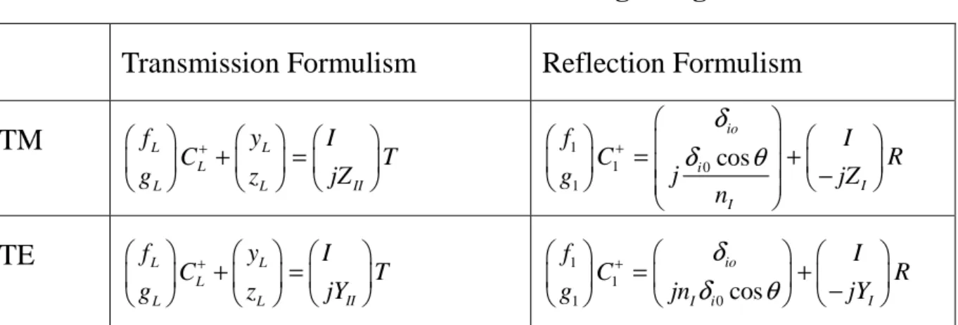
Table 2.1 Summary of full mathematic formulation for RCWA
Reflected and diffracted amplitudes are determined simultaneously by solving table 2.1 in either TE or TM mode. Another simpler and memory saving way is called partial solution approach. It employs the same concept of full mathematics method in a much more stable and efficient way with only half number of matrix multiplications needed comparing to full-solution approach. By solving the reflected and transmission diffraction mode separately, the size of matrix can also decrease into half. The partial solution formulism is listed in Table 2.2. Further deductions from Table 2.1 to Table 2.2 are proved in Appendix. 0 1 1 1 1 0 1 1 1 1 cos i i I I W W X C I R j jZ V V X C n δ δ θ +− + = − − 0 1 1 1 1 0cos 1 1 1 1 i I i W W X C I R jY j V V X C δ δ θ + − + = − − 1 1 1 1 1 1 1 1 l l l l l l l l l l l l l l l l W X W C W W X C V X V C V V X C + + − − − − − − − − − − = − −
Partial mathematic formulation for surface-relief grating
Transmission Formulism Reflection Formulism
TM L L L II L L f y I C T jZ g z + + = 1 1 0 1 cos io i I I f I C R j jZ g n δ δ θ + = + − TE L L L II L L f y I C T jY g z + + = 1 1 1 0cos io I I i f I C R jY g jn δ δ θ + = + −
Table 2.2 Summary of partial mathematic formulation for RCWA
2.2 Formulism in Computational Algorithm
2 0.3 2 0.3 T ( )Solar( ) Tsolar Solar( ) n i i d d λ λ λ λ λ =
∑ ∫
∫
(2.13) TSolar is defined as the ration of power penetrating at all diffraction orders over power incidence throughout wavelength of interest from 0.3um to 2um where GaInP/GaInAs/Ge solar cell dominates. Our goal is to find out the configuration for grating with highest Tsolar under 6000K solar spectrum. We then compile partial solution approach into mathematic software (Mathematica) and set up all the matrix formula in Table 2.2. The algorithm used to extract the optimized results utilized iterative method. Table 2.3 shows the computational process.Input environmental parameter
(
n h
d,
m, , , )
f
Λ
θ
iRCWA calculation for each diffraction order
(full or partial solution approach)
2 0.3 2 0.3 T (λ)Solar(λ) dλ TSolar= Solar(λ) dλ n i i
∑ ∫
∫
Extract diffraction efficiency of each order
Save and Change parameter
Export data and plot
loop
Computational algorithm
Chapter 3
Simulation Results and Analysis
3.1 Anti-Reflection Coating
We first design the anti-reflection coating (AR) using the program discussed in previous chapter, and assume TE and TM polarization being equally the same at normal incidence. Double-layer of SiO and 2 Si N AR 3 4 were adopted with refractive its index 1.54 and 2, respectively. SiO has 2 lower refractive index that is closer to the refractive index of air 1, therefore it is chose to stack on top. Also the refractive index for the substrate is 3.5.
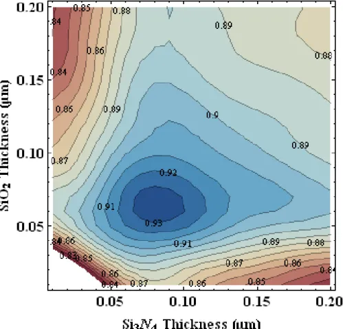
Figure 3.1 Contour map of transmittance under standard solar spectrum as functions of SiO2 and Si N3 4 thickness
The result is shown in figure 3.1, a contour map of Tsolar as function of
2
SiO and Si N3 4 thickness. This figure shows that maximum occurs at the
range where thickness of SiO2and Si N3 4 layers locate around 80 nm and 60
nm, respectively, with transmitted efficiencies over 93%. Although transmitted wavelength distribution of AR does not center at main peak of solar spectrum near 500 nm to 700 nm (figure 3.2), the total TSolar compared with no AR can still improve from 70%, to as high as 93.6%.
Figure 3.2 shows the comparison distribution of transmittance for surface with and without AR to normalized power density of black body radiation at 6000K as function of wavelength. Apparently, the total transmittance has been broadly improved.
Figure 3.2 The comparison of surface transmittance with and without AR to normalized black body power density at 6000K
0.5
1.0
1.5
2.0
0.0
0.2
0.4
0.6
0.8
1.0
0.0
0.2
0.4
0.6
0.8
1.0
Wavelength
l HÐm
LT
ra
n
sm
it
te
d
ef
fi
ci
en
cy
H % LN
o
rm
al
iz
ed
p
o
w
er
d
en
si
ty
H % L ARNormalized solar spectrum W/O AR
3.2 Sub-Wavelength Grating Structure
AR though well performs at normal incidence; it works only at a certain span of wavelength and incident angle. However, broad band characteristic of grating structure has been investigated and widely employed to the enhancement of light collection at oblique angle.
According to (2.3) if a grating with its period less than half the wavelength of incident light, only lower diffracted order will present and other higher orders are evanescent. This kind of grating is called sub-wavelength grating, and shown to contain broadband properties [9]. From theoretical consideration, if we only consider certain wavelength, eg. λ=600 nm, the depth of the grating has to be 300 nm with period 400 nm and filling factor 0.3 in order to achieve higher
0.0 0.2 0.4 0.6 0.8 1.0 94 95 96 97 98 99 100 Grating depth HHÐmL T ra n sm it te d ef fi ci en cy H % L Period 0.4um Filling Factor 0.3 TSolar λ λ λ λ 600 nm
Figure 3.3 The transmittance comparison of TSolar to wavelength 600 nm as function of grating depth, with period 0.4um, filling factor 0.3
transmittance over 98%. As for solar applications, it is more practical to value TSolar. Therefore the transmittance would be different when TSolar is taking into consideration. Figure 3.3 indicates the maximum transmitted efficiency is over 95% with the grating depth around 100 nm. Moreover, it is more feasible to produce a 100 nm depth grating than 300 nm.
Optimum grating configuration
To find out the optimum height, period and width of grating, approximations were made based on assumptions consistent with theory [9]. Typical value shows out the depth of grating, H, in the scale of nanometer is possible lower, and therefore we firstly fix H at certain theoretical expected values, which begins at lower limit of 50nm, and change the other two variables, period and width, to extract optimum parameter. We then increase H step by step and compare every optimum value in each run. H was roughly estimated using plot of comparison in Table 3.1, which demonstrates the reflectivity contour map of TSolar as functions of period and filling factor.
By increasing H every 50 nm each plot, a low value of reflectivity of less than 5% can only be obtained with 0.05µm< <H 0.25µm. Although the lowest peak of reflectivity shifts toward larger period and smaller filling factor with higher H, the fabrication process is relatively difficult and also the reflectivity are all over 5%. Additionally, a larger ratio of depth over period naturally results in a larger surface area, which increases the possibility of surface recombination in solar cells. In this aspect, it is inferred that with H 0.1µm , period 0.3~0.4 and filling factor 0.3~0.4 is effective for reducing the surface reflection loss without severe surface recombination loss.
Table 3.1
Contour Map of reflectivity of different height of grating H as functions of period and filling factor under the standard solar spectrum
H
0.05
µ
m
0.1µ
m
0.15um 0.2um
( ) ( )
0.25
µ
m
0.3µ
m
0.35
µ
m
0.4µ
m
( ) ( )
0.45um 0.5um
These values can be refined by iterative comparison, thus a preferable profile of grating is approximately chosen. We now fix the value of period to 0.35µm where indicated to have the lowest reflectivity in Table 1.1, and vary the depth and width of grating. The contour plot of transmittance at period 0.35µm as functions of grating depth and filling factor is shown in figure 3.4. The results turn out similar to previous estimation, that H around 0.1 µm and filling factor 0.3 marks the highest transmitted efficiency over 95%. It is noticeable that there is also another peak at higher depth and smaller filling factor exhibits to have transmitted efficiency over 94%. Unfortunately, due to the fabrication difficulties to produce a grating with depth 0.5µm 90 and width o
60 nm, we should focus more attention on the feasible outcome on the left side of figure 3.4.
Result of optimum grating structure
Consequently, the extraction of optimized filling factor and period had been determined. The results are shown in figure 3.5 below where the value of filling factor is 0.3 and period 0.35um which demonstrates the transmitted efficiency to be up to 95% at normal incidence. Finally, the optimum periodic 1D grating structure is then plotted in unit cell shown i n figure 3.6.
Figure 3.4 Contour map of transmittance under standard solar spectrum of grating period 0.35um as functions of height and FF
Figure 3.5 The optimum value of grating profile
Si3N4 60nm SiO2 80nm
SiO2 H=0.1um
W~100nm
Figure 3.7 compares the transmittance of two surface conditions with and without grating structure at normal incidence. Although the transmittance rate of surface with grating is not always surpass throughout the whole wavelength, it is the TSolar that plays a crucial parts and dominates throughout the whole incident angle in figure 3.8.
Figure 3.8 TSolar comparison of AR and Grating cell as function of incident angle 0.4 0.6 0.8 1.0 1.2 1.4 1.6 1.8 0.80 0.85 0.90 0.95 1.00 Wavelength lHÐmL T ra n sm it te d ef fi ci en cy
Figure 3.7 Transmittance comparison of sample with AR and grating as function of wavelength AR Grating 0 20 40 60 80 0.5 0.6 0.7 0.8 0.9 1.0 Incident angle q T S o la r tr an sm it ta nc e AR Grating
æææææææææææ æææ ææ æææææ æææ ææææ ææææææææææææææææææææææ æææ ææ ææ ææ ææ æ æ æ æ æ æ æ æ æ æ æ æ æ æ æ æ æ ææ æææ æ æ æ æ æ æ æ 0 20 40 60 80 0 1 2 3 4 5 Incident angleq D T S o la r tr an sm it ta n ce H % L
3.3 Broadband Characteristic at Oblique incidence
As expected the broadband absorption at oblique incidence, figure 3.9 shows the subtraction between two curves in figure 3.8. It indicates the enhancement effect is stronger (> 5%) at higher incident angle. This improvement can be contributed to the geometric form of grating. Figure 3.10 shows the distribution of TE and TM polarization to TSolar throughout whole incident angle. TE modes decade faster than TM at higher incidence, while TM modes compensate the reflection loss caused by TE polarization.
0 20 40 60 80 0.4 0.5 0.6 0.7 0.8 0.9 1.0 Incident angleq T S o la r tr an sm it ta n ce TE TM Total
Figure 3.9 The TSoalr difference between sample with and without grating
Figure 3.10 The contribution of TE & TM modes to TSolar as function of incident angle
Wavelength distribution at different incident angle
Figure 3.11.a and 3.11.b shows the transmittance distribution of each wavelength at various incident angles with AR on the surface and AR with grating on the surface, respectively.
(a) (b)
At the span of short wavelength, the transmittance in figure 3.11 (b) has better performance over 6% until 60 degree incident comparing to figure 3.11 (a). Throughout the middle span of wavelength between 0.6 µm to 1.2 µm , (b) can still suppress more than 2% at oblique incident.. It is also obvious to mention that transmittance raises invigorately more than 20%.. at larger incident angle. We then expect the increasing amount of light will successfully form Figure 3.11 Contour map of transmittance of (a) AR and (b) AR with grating structure
electron-hole pairs and contribute to the improvements of photovoltaic energy conversion efficiencies.
As expected for sub-wavelength grating where only lower transmission order exist, figure 3.12 displays the TSolar transmitted distributions for different diffractive order of both TE and TM polarization, as function of incident angle. The light is almost diffracted into zero order, as well as at higher incidence, with only a partial portion of light parcel into first order.
0 20 40 60 80 q 0.0 0.2 0.4 0.6 0.8 1.0 Ts TM
Figure 3.12 Displays of the transmittance diffractive order distributions as function of incident angle in TM(left) and TM(right) polarization
0 20 40 60 80 q 0.0 0.2 0.4 0.6 0.8 1.0 Ts TE Total 0 order Higher order
Chapter 4
Experimental Analysis and Discussion
4.1 Sample Design and Fabrication Process
The sample used here is InGaP/InGaAs/Ge triple junction solar cell provided by Visual Photonics Epitaxy Co. (VPEC). The structure is schematically shown in figure 4.1.
In order to compare the effect of grating structure after realizing it onto surface of solar cell, three kinds of device will be made, including device without AR coating, with AR coating and with grating on top after AR coating. The standard process for these three kinds includes:
(1)Step 1: Photo lithography for electrode pattern. (figure 4.2)
To reduce the series resistance between grid electrode, it is evaluated by using equivalent circuit model in figure 1.9 and calculate by certain simulation program [27,28]. Therefore, the suitable configuration of electrode contact can be designed with grid width 5 µmand pitch 112 µminside 1mm square and the total shadow loss due to contact coverage
is about 5%. Moreover the ohmic contact resistance can sufficiently be reduced by depositing Ni/Ge/Au alloy onto highly doping N -InGaAs+ layer and Ti/Au alloy on P -Ge+ substrate. After evaporating electrodes, the device then put to annealing at 400°C for 30 seconds. It is requisite to etch off the N+capping layer with certain kinds of acid solvents [29] and to expose AlInP window layer before depositing AR coating. The acid solution used here is H SO , H O , H O2 4 2 2 2 (1:8:80).
The device without AR is done and shown in figure 4.3. We then proceed to the second kind of device where AR coating is deposited on top of surface.
(2)Step 2: Anti-reflection coating. (figure 4.4)
Two flat dielectric AR coating layers, Si N3 4 and SiO2, are deposited, at the optimized thickness, 60nm and 80nm respectively by using PECVD technique. By using BOE solvent, the electrode covered by AR
can be revealed. Be sure to make the soaking time inside BOE as precise as possible, thus lowering the risk of any chance for lateral penetration which might damage the wafer.
The second kind of device is done and shown in figure 4.5. Lastly, we will continue to put the grating structure onto AR layer. The fabrication of grating structure in the scale of nanometer can not be completed using photo-lithography. Consequently, E-beam lithography technique is introduced to pattern the period structure.
(3)Step 3: E-beam lithography for sub-wavelength grating. (figure 4.6) As a result of the optimization in chapter 3, the period and width of the grating are designed to be 350nm and 100nm respectively. PMMA is a high contrast positive resist and has good adhesion on nearly any surface, thus has been widely applied for nano-lithography. During the process, it is better to create an undercut profile on resist, thus making it easier to life-off. To perform such undercut profile, it requires two layers of PMMA with different solvent concentration, A3 and A5. Due to the different dissolution properties from each layer, undercut can be made as controlling the developing time carefully by means of develop solvent MIBK (figure 4.6.1). Afterwards the 100 nm thicknesses of SiO2 gratings are thermally evaporated using E-gun (figure 4.6.2), and lift-off process can be easily done when soaking in acetone without further agitation (figure 4.6.3).
Figure 4.7 shows the top view of SEM image. We also obtain different width from 100nm to 150nm. Therefore, further investigations of the effect caused by various width of grating can also be discussed in the following section.
mask 5214E substrate Exposure N-type Metal Ni/Ge/Au Lift off
Step 1 Photolithography for electrode
Anneal 400°C 1mm Develop AZ 300 P-type Metal Ti/Au Ni/Ge/Au Ti/Au A. Metal Contact
B. Etch capping layer
Solution H SO :H O :H O=1:8:802 4 2 2 2
TOP VIEW
Figure 4.2 Photo lithography process for electrode pattern
Figure 4.3 Electrode contact configuration
1mm
5um
+
N InGaAs cap layer 0.5um
STEP 2 AR Coating PECVD coating 2 SiO 3 4 Si N BOE etch AR Top view
Figure 4.4 Anti-reflection coating process
Figure 4.5 Electrode contact configuration after removing AR by using acid BOE
44
Step 3 E Beam Lithography
sample PMMA-A3 PMMA-A5 E Beam Exposure Develop MIBK A. Grating pattern set
sample
B. E-GunSiO2Coating
sample
Lift off
sample 100nm
After E-beam exposure
Deposit SiO2 Figure 4.6.1 After lift off
Figure 4.6.2 Figure 4.6.3
Figure 4.7 Top view of SEM image of grating with period 350nm, depth100nm and width 100nm under (a) large scale (b) small scale
(a)