國 立 交 通 大 學
顯 示 科 技 研 究 所
碩士論文
分散式控制混合型被動光纖網路之
光網路單元設計
Optical Network Unit Design for Novel
Distributed Control Hybrid Passive
Optical Network
研
究
生 : 曹 正
分散式控制混合型被動光纖網路之
光網路單元設計
Optical Network Unit Design for Novel
Distributed Control Hybrid Passive Optical
Network
研 究 生 :曹正
Student :
Cheng
Tsao
指導教授 :陳智弘 老師
Advisor :
Associate
Prof. Jyehong Chen
國 立 交 通 大 學
顯 示 科 技 研 究 所
碩 士 論 文
A Thesis
Submitted to Institute of Electro-Optical Engineering
College of Electrical Engineering and Computer Science
National Chiao Tung University
In Partial Fulfillment of the Requirements
For the Degree of
Master
In
Display Institute
July 2007
Hsinchu, Taiwan, Republic of China
A
CKNOWLEDGEMENTS 很快的,兩年過去了。能夠完成碩士的學業,我最要感謝的就是我的指導教 授,陳智弘老師。老師的因循善誘,並在研究上給予許多的自由,使我這兩年能 學習如何自己分配時間,在壓力最小的情況下順利完成碩士論文。除了專業領域 的幫助,陳老師生活態度也使我收穫良多。 感謝清雲學長以及玉民學長在程式、通訊領域、實驗硬體等各方面給予許多 的幫助,清雲學長更不厭其煩的陪我們度過最難熬的最後這幾個月,帶我們做實 驗、幫我們改程式。沒有他們我無法完成我的碩士論文。 感謝帶領我進入這實驗室的小強,使我成為實驗室第一位顯示所的學生。多 年來他一直成為我生活上的諮詢對象,對我的人生有很大的影響。感謝嘉建、彭 煒仁、俊廷、昇祐、小雨在這兩年的照顧,在實驗以及生活上都給了我許多的指 教。 感謝實驗室成員,教練、晟峰以及俊臻,他們的陪伴使我的碩士生涯更添色 彩,並且在互相的討論中,讓我學習到更多;實驗室的學弟文翔、易辰、盛鵬、 小江以及小高,使實驗室整個熱鬧起來。 最後,我最重要的家人,我的父、母親、還有妹妹,感謝他們的包容,並讓 我有一個溫暖的家。 曹正 2007/07/20分散式控制混合型被動光纖網路之光網路
單元設計
學生:曹正 指導教授 : 陳智弘 老師
國立交通大學顯示科技研究所碩士班
摘要
近幾年來,由於網際網路以及全球資訊網(WWW)的普及,以往的影
音、數據導向的存取網路系統漸漸轉化為視頻、影像為主體。使用點
對多點架構的被動光纖網路,因其提供了很大的頻寬及很快的傳送速
度(>100 Mb/s)而受到極大的重視。然而傳統分波多工、分時多工的
系統因為封包來回時間太長而使封包延遲,常導致頻寬被浪費掉。
在本篇論文中,我們介紹一個分散式控制混合型光纖被動網路系
統(DHPON)。這個新架構包含了分時多工還有分波多工兩種技術,並
在數個光網路單元中進行分散式的動態頻寬分配。我們並自己設計光
線路終端以及光網路單元,因此我們可以實際架起一個 DHPON 系統。
本篇論文將主要說明光網路單元的部分。
Optical Network Unit Design for Novel
Distributed Control Hybrid Passive Optical
Network
Student:Cheng Tsao Advisor : Dr. Jyehong Chen
Display Institute
National Chiao Tung University
Abstract
In recent years, voice- and text-oriented services have evolved to data- and image-based services due to popularity and growth of the internet and worldwide web (WWW). Passive optical network, which uses a point-to-multipoint architecture, have attract much attention since it provides high bandwidth and high speed (>100 Mb/s). However, traditional WDM and TDM PON have some disadvantage that the packet delay occur due to large round trip time (RTT) , thus result in bandwidth sometimes been wasted.
In this thesis, we introduce a new architecture – Distributed-control Hybrid Passive Optical Network (DHPON). This new architecture contains both TDM and WDM system and a new distributed-control DBA is worked among several ONU that reduce the RTT. We also design the Optical Line Terminal (OLT) and Optical Network Unit (ONU) that we can really set up a DHPON scheme.
C
ONTENTSAcknowledgements
... iChinese Abstract
... iiEnglish Abstract
... iiiContents
... ivList of Figures
... viiList of Tables
... viiiCHAPTER 1
Introduction
1.1 Access Network Overview ...11.2 Passive Optical Network...2
CHAPTER 2
Distributed Control Hybrid Passive Optical Network
2.1 TDM and WDM PON...42.1.1 Time Division Multiplexing PON...4
2.1.2 Wavelength Division Multiplexing PON...5
2.2 Distributed-control Hybrid Passive Optical Network (DHPON) ...6
2.2.1 Interleaved Polling with Adaptive Cycle Time (IPACT) ...6
2.2.2 DHPON...9
2.3 DHPON versus IPACT ... 11
2.3.1 Packet mean Delay... 11
2.3.2 Packet drop rate...12
CHAPTER 3
Simulations
3.1 Simulation Methods ...143.1.2 Xilinx Project Navigator ...15
3.1.3 Synplify Pro ...15
3.1.4 Modelsim ...16
3.1.5 Flow Diagram ...16
3.2 PHY、Serdes and MII...18
3.2.1 Physical Layar...18
3.2.2 Serdes...19
3.2.3 Medium Independent Interface ...19
3.3 Up Stream ...20 3.3.1 Ethernet MAC...20 3.3.2 Buffers...21 3.3.3 Bridge...26 3.3.4 Framer ...26 3.3.5 DBAcontrol...28 3.3.6 Simulation Result...29 3.4 Down Stream ...31 3.4.1 PON MAC ...32 3.4.2 BufferO ...35 3.4.3 Outcontrol ...36 3.4.4 Simulation Result...37
CHAPTER 4
OnBoard Testing
4.1 Field Programmable Gate Array (FPGA) ...394.2 ONU Board ...40
4.3 Testing Result...41
4.3.2 Down Stream ...47
CHAPTER 5
Conclusions
5.1 DHPON...49 5.2 Future work...49
L
IST OFF
IGURESFigure 1.1 Access network and PON architecture ...3
Figure 2.1 Architecture of TDM-PON...4
Figure 2.2 Architecture of WDM-PON ...6
Figure 2.3 Centralized-Control DBA...7
Figure 2.4 Example of IPACT ...8
Figure 2.5 Architecture of DHPON ...9
Figure 2.6 Distributed-control DBA : concept...10
Figure 2.7 Simulation result of DHPON vs IPACT (packet mean delay) ...12
Figure 2.8 Simulation result of DHPON vs IPACT (packet drop rate) ...13
Figure 3.1 Xilinx Project Navigator...15
Figure 3.2 Flow diagram for OLT...17
Figure 3.3 Flow diagram for ONU ...17
Figure 3.4 Header of upstream packet(above) and downstream packet(below).18 Figure 3.5 Simulation results for Ethernet MAC...21
Figure 3.6 Dual-port block memory ...23
Figure 3.7 Simulation result for buffer0 ...24
Figure 3.8 Simulation result for buffer3 ...26
Figure 3.9 Simulation result for framer ...28
Figure 3.10 RTL scheme of the full upstream module ...29
Figure 3.11 Simulation result for full upstream module after post-place & route (input)...30
Figure 3.12 Simulation result for full upstream module after post-place & route (header of output)...30
Figure 3.13 Simulation result for full upstream module after post-place & route (end of packet) ...31
Figure 3.14 Simulation results for corrector ...33
Figure 3.15 Simulation results for main PON MAC ...34
Figure 3.16 Simulation results for bufferO. Above : input situation ...35
Below : MAC address is shown...35
Figure 3.17 Simulation results for BufferO (output situation) ...36
Figure 3.18 Simulation results for outcontrol ...37
Figure 3.19 RTL scheme of the full downstream module...38
Figure 3.20 Simulation result for full downstream module after post-place & route ...38
Figure 4.1 ONU Board front view ...40
Figure 4.2 Logic Analyzer ...42
Figure 4.3 LA Probes ...42
Figure 4.4 Ethernet Packet...43
Figure 4.5 Packet has been separated into slots...44
Figure 4.6 The header ...44
Figure 4.7 Data of the slot...45
Figure 4.8 The end of the packet ...45
Figure 4.9 Next packet comes in...46
Figure 4.10 60 bytes packet ...46
Figure 4.11 Data sent into the down stream module...47
Figure 4.12 MAC address of output data...48
Figure 4.13 Output data ...48
L
IST OFT
ABLES Table 4-1 ONU specification………. .40CHAPTER 1
I
NTRODUCTION1.1 Access Network Overview
The access network, connect business and residential subscribers to the central
offices of service providers, which in turn are connected to metropolitan area networks (MANs) or wide area networks (WANs). Access networks are commonly referred to as the last mile or first mile; the latter term emphasizes their importance to subscribers.
The predominant broadband access solutions deployed today are the digital subscriber line (DSL) and community antenna television (CATV) (cable TV) based networks. However, both of these technologies have limitations because they are based on infrastructure that was originally built for carrying voice and analog TV signals, respectively; but their retrofitted versions to carry data are not optimal. Currently deployed blends of asymmetric DSL (ADSL) technologies provide 1.5 Mbits/s of downstream bandwidth and 128 Kbits/s of upstream bandwidth at best. Moreover, the distance of any DSL subscriber to a CO must be less than 18000 ft because of signal distortions. Although variations of DSL such as very-high-bit-rate DSL (VDSL), which can support up to 50 Mbits/s of downstream bandwidth, are gradually emerging, these technologies have much more severe distance limitations.
For example, the maximum distance over which VDSL can be supported is limited to 1500 ft. CATV networks provide Internet services by dedicating some radio frequency (RF) channels in a coaxial cable for data. However, CATV networks are mainly built for delivering broadcast services, so they don’t fit well for the bidirectional communication model of a data network. At high load, the network’s performance is usually frustrating to fend users [1]. These access technologies are
unable to provide enough bandwidth to current high-speed Gigabit Ethernet local area networks (LANs)[2] and evolving services (e.g., distributed gaming or video on demand)[3].
In so-called FTTx access networks the copper-based distribution part of access networks is replaced with optical fiber; for example, fiber to the curb (FTTC) or home (FTTH). In doing so, the capacity of access networks is sufficiently increased to provide broadband services to subscribers. Due to the cost sensitivity of access networks, these all-optical FTTx systems are typically unpowered and consist of passive optical components (e.g.,, splitters and couplers). Accordingly, they are called passive optical networks (PONs).
Recent developments in telecommunications have produced greatly increased capacity in backbone networks. While the capacity of backbone networks has largely kept pace with the tremendous growth of Internet traffic, there has been little progress in the access network, the so-called last mile, where a bottleneck occurs between the backbone network and the high-capacity local area networks. The only effective solution to this last mile bottleneck is a universal fiber-based infrastructure that is accessible to both businesses and residences. The PON technology is viewed by many as an attractive solution to the last mile problem [4], [5].
1.2 Passive Optical Network
A Passive Optical Network (PON) is a single, shared optical fiber that uses inexpensive optical splitters to divide the single fiber into separate strands feeding individual subscribers. PONS are called "passive" because, other than at the CO and subscriber endpoints, there are no active electronics within the access network [6]. The main advantage of PON is that it requires less wiring than point to point, that it mutualises the service for several subscribers, and that it has no active element
beyond the central exchange, in other words, only optical fibers and optical passive elements do not require any electrical power or active management. In addition, the lifetime of the outside passive plant should be greater than 25 years to justify the installation costs and maximize the savings in operational expenses.
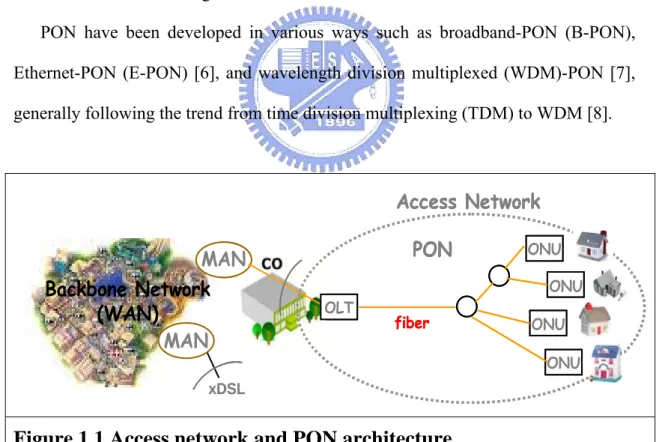
A PON network includes an optical line terminal (OLT) and an optical network unit (ONU). The OLT resides in the CO (POP or local exchange). This would typically be an Ethernet switch or Media Converter platform. The ONU resides at or near the customer premise. It can be located at the subscriber residence, in a building, or on the curb outside. The ONU typically has an 802.3ah WAN interface, and an 802.3 subscriber interface. We can see in figure1.1, the OLT is on the left and several ONUs are shown on the right.
PON have been developed in various ways such as broadband-PON (B-PON), Ethernet-PON (E-PON) [6], and wavelength division multiplexed (WDM)-PON [7], generally following the trend from time division multiplexing (TDM) to WDM [8].
Backbone Network
(WAN)
MAN
xDSLAccess Network
MAN
PON
fiber OLT ONU ONU ONU ONUBackbone Network
(WAN)
MAN
xDSLAccess Network
MAN
PON
fiber OLT ONU ONU ONU ONUCHAPTER 2
D
ISTRIBUTEDC
ONTROLH
YBRIDP
ASSIVEO
PTICALN
ETWORK2.1 TDM and WDM PON
2.1.1 Time Division Multiplexing PON
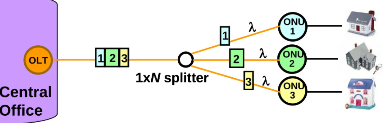
TDM-PONs have a long development history with examples such as APON, BPON, EPON and GPON. The main concept behind the TDM approach is to use a single high-performance shared transceiver at the central office to communicate with the “N” remote ONU transceivers. This approach requires the use of a 1xN power splitter to divide the optical power equally between the multiple ONUs. Since each remote ONU uses the same upstream wavelength, they must all take turns using dedicated and variable time slots where only a single ONU is allowed to transmit. A relatively complex processor located at the OLT controls the management and assignment of these individual transmission time slots. In the downstream direction a single data wavelength is used to broadcast to all the users. The ONUs identify their specific data packets by address information located in the header bit streams [9].
ONU 1 ONU 2 ONU 3
λ
OLTλ
λ
1xN splitter
1 2 3 1 2 3Central
Office
ONU 1 ONU 2 ONU 3λ
OLTλ
λ
1xN splitter
1 2 3 1 2 3Central
Office
Figure 2.1 Architecture of TDM-PON
This traditional single-wavelength PONs combine the high capacity provided by optical fiber with the low installation and maintenance cost of a passive infrastructure. The optical carrier is shared by means of a passive splitter among all the subscribers. As a consequence, the number of ONUs is limited because of the splitter attenuation and the working bit rate of the transceivers in the central office (CO) and in the ONUs. Current specifications allow for 32 ONUs at a maximum distance of 20 km from the OLT and 64 ONUs at a maximum distance of 10 km from the OLT. A WDM-PON solution provides scalability because it can support multiple wavelengths over the same fiber infrastructure, is inherently transparent to the channel bit rate, and it does not suffer power-splitting losses, as will be explained below.
2.1.2 Wavelength Division Multiplexing PON
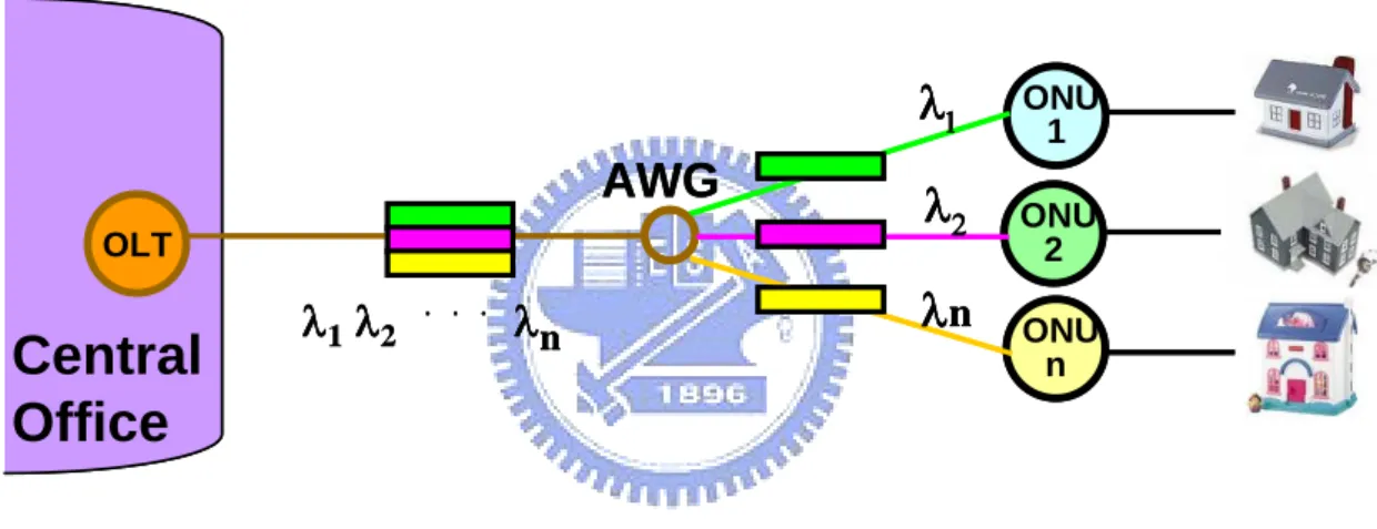
The straightforward approach to build a WDM-PON [1] is to employ a separate wavelength channel from the OLT to each ONU, for each of the upstream and downstream directions. This contrasts to the TDMA case where a single pair of wavelengths is shared among all the subscribers connected to the PON. This means that each user can send data to the OLT at any time, independent of what the other users are doing. In other words, there is no interaction or coupling between the subscribers on a WDM-PON; this eliminates any management issues related to sharing the PON. Each subscriber gets a dedicated point-to-point optical channel to the OLT, although they are sharing a common point-to multipoint physical architecture [10]. Also, each ONU can operate at a rate up to the full bit rate of a wavelength channel. Moreover, different wavelengths may be operated at different bit rates, if necessary; hence, different varieties of services may be supported over the same network. In other words, different sets of wavelengths may be used to support different independent PON sub-networks, all operating over the same fiber
infrastructure.
In the downstream direction of the WDM-PON (Fig4.2), the wavelength channels are routed from the OLT to the ONUs by a passive arrayed waveguide grating (AWG) router, which is deployed at a “remote node” (RN), which is where the passive splitter used to be in a TDM-PON. For the upstream direction, the OLT employs a WDM demultiplexer along with a receiver array for receiving the upstream signals. Each ONU is equipped with a transmitter and receiver for receiving and transmitting on its respective wavelengths.
Central
Office
ONU 1 ONU 2 ONU nAWG
OLTλ
2λn
λ
1λ
1λ
2 ...λ
nCentral
Office
ONU 1 ONU 2 ONU nAWG
OLTλ
2λn
λ
1λ
1λ
2 ...λ
nFigure 2.2 Architecture of WDM-PON
2.2 Distributed-control Hybrid Passive Optical Network (DHPON)
2.2.1 Interleaved Polling with Adaptive Cycle Time (IPACT)
In a TDM system, The long-range dependence (heavy-tailedness) of the traffic results in a situation where some timeslots overflow even under very light load resulting in packets being delayed for several timeslot periods. It is also true that some timeslots remain underutilized (not filled completely) even if the traffic load is very high. That leads to the PON bandwidth being underutilized.
A dynamic scheme that reduces the timeslot size when there is no data would allow the excess bandwidth to be used by other ONUs. We called it a Dynamic
bandwidth allocation (DBA) [11]. The challenge of implementing such a scheme is in the fact that the OLT does not know exactly how many bytes of data each ONU has. If the OLT is to make an accurate timeslot assignment, it should know exactly how many bytes are waiting in a given ONU.
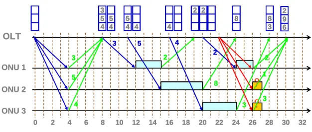
We use a centralized-control DBA to solve this situation. The prevailing method of centralized-control DBA scheme is Interleaved Polling with Adaptive Cycle Time (IPACT) [12]. In a IPACT scheme, every ONU, before sending its data, will send a special message announcing how many bytes it is about to send. This Buffer information of ONUi is transmitted again at the end of its data packets, as we can see in figure2.3. The ONU that is scheduled next (say, in round-robin fashion) will monitor the transmission of the previous ONU and will time its transmission such that it arrives to the OLT right after the transmission from the previous ONU. Thus, theoretically, there will be no collision and no bandwidth will be wasted.
ONU 1 ONU 2 ONU 3 OLT 1xN Splitter
1
2
Buffer size of ONU 1
Round Trip Time = Times for information from ONU to OLT and again back to ONU
1
3
of ONU 2 Of ONU 3 ONU 1 ONU 2 ONU 3 OLT 1xN Splitter1
2
Buffer size of ONU 1
Round Trip Time = Times for information from ONU to OLT and again back to ONU
1
3
of ONU 2 Of ONU 3
Figure 2.3 Centralized-Control DBA
On the other hand, the main disadvantage of IPACT lies in the fact that packets that arrived outside of the time slot are not taken into account during the bandwidth allocation process and must wait until the next cycle, thus experiencing much larger
2 4 6 8 10 12 14 16 18 20 22 24 26 28 30 32 0 3 2 2 5 4 5 4 5 4 8 8 4 4 3 8 3 3 5 4 3 5 4 2 2 2
?
1?
3 OLT ONU 1 ONU 2 ONU 3 2 9 6 2 4 6 8 10 12 14 16 18 20 22 24 26 28 30 32 0 2 4 6 8 10 12 14 16 18 20 22 24 26 28 30 32 0 3 2 2 5 4 3 2 2 2 5 4 5 4 5 4 5 4 8 8 5 4 4 5 4 5 4 8 8 8 4 4 3 8 3 4 4 4 3 8 3 8 3 3 5 4 3 5 4 3 5 4 3 5 4 3 5 4 2 2 2 2 2 2 2?
1?
1?
3?
3 OLT ONU 1 ONU 2 ONU 3 2 9 6 2 9 6Figure 2.4 Example of IPACT
message will be delayed because the round trip time is also long. As a result, we might get empty time slots and thus waste the bandwidth. We can see a simple example in figure2.4, assume the RTT is 8 time slots in this case. It takes 8 time slots for OLT to get the queue sizes of each ONU. Then another 4 time slots to send control message to ONU1. While ONU start to send data, it is 12 time slots later. After that, OLT continue to give control message and receive queue sizes from each ONU. It seems that the TDM works well until we can see in the right of figure2.4, because the polling table cannot update efficiently, after 2 time slots are used by ONU1, the polling table in OLT are all empty now thus OLT cannot send control message to ONUs until OLT again receive queue size message from ONUs. During these time slots, the bandwidth is wasted because no data are transmitting. Also during these times, data continue to send to the buffer of each ONU. The data now accumulate there in the buffer. This situation causes a severe problem that we cannot send the data out efficiently. Therefore we now need a new method to work the DBA efficiently.
2.2.2 DHPON
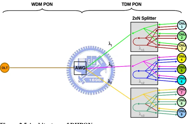
A new scheme of Distributed-control Hybrid Passive Optical Network (DHPON) is proposed here. It is hybrid because the TDM and WDM system is combined in this scheme. On the other hand, we use a distributed-control DBA that runs the DBA algorithm. ONU 1 ONU 2 ONU 3 2xN Splitter AWG OLT λ2 λ3 λ1 WDM PON TDM PON ONU 4 ONU 5 ONU 6 ONU 7 ONU 8 ONU 9 λc1 λc2 λc3 ONU 1 ONU 2 ONU 3 2xN Splitter AWG OLT λ2 λ3 λ1 WDM PON TDM PON ONU 4 ONU 5 ONU 6 ONU 7 ONU 8 ONU 9 λc1 λc2 λc3
Figure 2.5 Architecture of DHPON
DHPON architecture is shown in figure2.5, each sub-PON we assign a wavelength. Thus by using a WDM system, we can have several sub-PON. In each sub-PON, it is operated under a TDM system scheme. The bandwidth can be fully shared in sub-PON because DBA will assign bandwidth (time slot) to ONUs.
However, this scheme offers many ONUs, the situation become complicated since in the traditional centralized-control DBA, a few ONUs can cause severe time delay, and now we have a lot. Therefore, DHPON solve this trouble that we present a
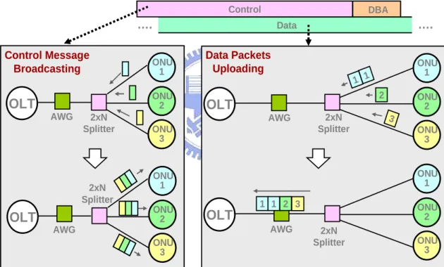
distributed-control DBA. As we can see in figure2.5, Each ONU transmits its data traffic with λ1 (high data rate). On the other hand, Each ONU transmits its update control message with λc1 (low data rate). A basic concept of DHPON is shown in figure2.6. The control message contains queue size information of ONU and are redirected back broadcasting to all ONUs. It is important to note that data traffic and control messages are transmitted independently, thus the queue sizes of ONUs are updated efficiently. After receiving the broadcast control message, based on the same DBA algorithm, each ONU computes its starting time and the time slots of packets.
OLT ONU 1 ONU 2 ONU 3 OLT ONU 1 ONU 2 ONU 3 OLT ONU 1 ONU 2 ONU 3 2 1 1 3 Data OLT ONU 1 ONU 2 ONU 3 1 3 DBA 2xN Splitter 2xN Splitter 2xN Splitter 2xN Splitter AWG AWG AWG AWG …. …. Control 1 2 Control Message Broadcasting Data Packets Uploading OLT ONU 1 ONU 2 ONU 3 OLT ONU 1 ONU 2 ONU 3 OLT ONU 1 ONU 2 ONU 3 2 1 1 3 Data OLT ONU 1 ONU 2 ONU 3 1 3 DBA 2xN Splitter 2xN Splitter 2xN Splitter 2xN Splitter AWG AWG AWG AWG …. …. Control 1 2 Control Message Broadcasting Data Packets Uploading
Figure 2.6 Distributed-control DBA : concept
In this scheme, each sub-PON runs the DBA independently. Therefore although we have many ONUs there, the number of ONUs that DBA deal with is not that large. Thus, by using a distributed-control DBA, the TDM system can operate efficiently. Also, by using a WDM system, one OLT can deal with many ONUs with no timing delay and bandwidth wasting.
2.3 DHPON versus IPACT
In the previous section, we introduce the advantages of the new scheme we have proposed. However, since this DHPON has not really set up, we do not know if this scheme does work well. In this section, some simulations have already been done to prove that our DHPON does work and the behavior had a tremendous improve comparing to traditional IPACT.
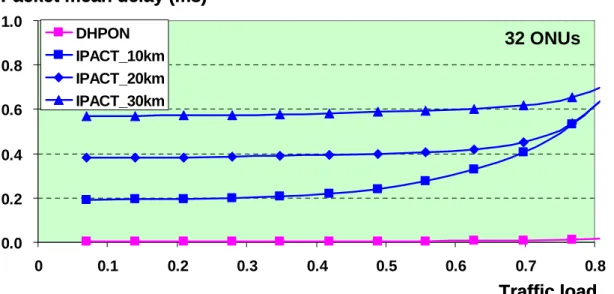
2.3.1 Packet mean Delay
We now compare the packet mean delay between DHPON and IPACT. We assume a 32 ONUs scheme and are operated under different traffic load. As we can see in figure2.7, we have IPACT(centralized-control) which the distance between ONU and OLT are 10km, 20km, 30km. The figure shows that even under low traffic load, an IPACT still cause huge delay. Also a long distance IPACT shows more delay than the other short distance IPACT. So we know that distance issue really effect a lot to an IPACT scheme. However DHPON shows nearly zero time delay. At high traffic load, we can see the delay become severe at all IPACT cases. Even a shorter distance IPACT shows very large timing delay. On the other hand, DHPON remains a low delay while the traffic load is increasing. We can see that even in the highest traffic load of this simulation, the delay for DHPON is just a little increased.
The simulation shows that DHPON does solve the problem that huge timing delay might occur because of the distance between the ONU and OLT. Under this scheme, the traffic goes efficiently compare to the old scheme. Another important issue is considered that a packet drop rate is also simulated and presented in the next section.
0.0 0.2 0.4 0.6 0.8 1.0 0 0.1 0.2 0.3 0.4 0.5 0.6 0.7 0.8 DHPON IPACT_10km IPACT_20km IPACT_30km Traffic load Packet mean delay (ms)
32 ONUs 0.0 0.2 0.4 0.6 0.8 1.0 0 0.1 0.2 0.3 0.4 0.5 0.6 0.7 0.8 DHPON IPACT_10km IPACT_20km IPACT_30km Traffic load Packet mean delay (ms)
32 ONUs
Figure 2.7 Simulation result of DHPON vs IPACT (packet mean
delay)
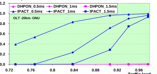
2.3.2 Packet drop rate
Packet drop rate means that each packet we assign a packet lifetime, if a timing delay is over some mini-second that larger than the packet lifetime, the packet is dropped. We assume again a 32 ONUs scheme operated under a 20 km OLT to ONU distance IPACT and a DHPON. We can see the cases in figure2.8, if the delay is over 0.5ms or 1ms or 1.5ms, according to different traffic load, we can get different drop rate. The result shows that at low lifetime IPACT, even the traffic load is also low, however it suffer severe packet drop problem. A longer life time IPACT could have low drop rate in low traffic load. However, when the traffic load is increasing, the drop rate increase tremendously. When the traffic load is up to one, the drop rate also goes to one. That means that all nearly all the packets are dropped. We can give a conclusion that real time traffic can not satisfy under centralized-control.
On the other hand, no matter what the packet lifetimes are, DHPON always show a low drop rate very close to zero. Even when the traffic load is high, the packet drop rate seems no increasing in the figure. Therefore we can say that under a DHPON
scheme, nearly no packet will be dropped. 0.0 0.2 0.4 0.6 0.8 1.0 1.2 0.72 0.76 0.8 0.84 0.88 0.92 0.96
DHPON_0.5ms DHPON_1ms DHPON_1.5ms IPACT_0.5ms IPACT_1ms IPACT_1.5ms
Traffic load Packet drop rate
OLT -20km- ONU 0.0 0.2 0.4 0.6 0.8 1.0 1.2 0.72 0.76 0.8 0.84 0.88 0.92 0.96
DHPON_0.5ms DHPON_1ms DHPON_1.5ms IPACT_0.5ms IPACT_1ms IPACT_1.5ms
Traffic load Packet drop rate
OLT -20km- ONU
Figure 2.8 Simulation result of DHPON vs IPACT (packet drop rate)
The discussion about DHPON all point that this scheme does work well compare to the traditional centralized-control scheme. Now, we will start to set up a real DHPON and shows that we can operate it in real world.
CHAPTER 3
S
IMULATIONS3.1 Simulation Methods
In electronics, a hardware description language or HDL is any language from a class of computer languages for formal description of electronic circuits. It can describe the circuit's operation, its design and organization, and tests to verify its operation by means of simulation [14].
The program we use is Verilog HDL, which is commonly used today. To know the program is work or not, since working on board take lot of time, we first simulate in computer. We use software called Xilinx Project Navigator to write the program. Synplify Pro then compiles and synthesizes the program. After these work, we write a test bench file to send data into our input. Modelsim then shows the result for us, finally we can check the function we want does work or not.
3.1.1 Verilog HDL
Verilog is a hardware description language (HDL) used to model electronic systems. The language (sometimes called Verilog HDL) supports the design, verification, and implementation of analog, digital, and mixed-signal circuits at various levels of abstraction.
The designers of Verilog wanted a language with syntax similar to the C programming language so that it would be familiar to engineers and readily accepted. A subset of statements in the language is synthesizable. If the modules in a design contain only synthesizable statements, software can be used to transform or synthesize the design into a netlist that describes the basic components and connections to be implemented in hardware. The netlist may then be transformed into, for example, a
form describing the standard cells of an integrated circuit or a bitstream for a programmable logic device [15].
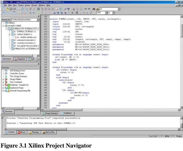
3.1.2 Xilinx Project Navigator
Xilinx Project Navigator is an Integrated Development Environment for digital logic design projects with Xilinx FPGAs and CPLDs. Project Navigator provides user windows displaying project hierarchy and the design process, as well as a context- sensitive HDL Editor [16].
Figure 3.1 Xilinx Project Navigator
3.1.3 Synplify Pro
The Synplify solution is a high-performance, sophisticated logic synthesis engine that utilizes proprietary Behavior Extracting Synthesis Technology to deliver fast,
highly efficient FPGA and CPLD designs. The Synplify product takes Verilog and VHDL Hardware Description Languages as input and outputs an optimized netlist in most popular FPGA vendor formats [17].
The main function of Synplify Pro lies in changing HDL into logic gate that FPGA chip needs, and will simplify Logic Gate that needn't be wanted in the course of changing, Its file outputted can let Xilinx Foundation continue doing the work of Place & Route .
3.1.4 Modelsim
ModelSim is an application that integrates with Xilinx ISE to provide simulation and testing tools. Two kinds of simulation are used for testing a design: functional simulation and timing simulation. Functional simulation is used to make sure that the logic of a design is correct. Timing simulation also takes into account the timing properties of the logic and the FPGA, so you can see how long signals take to propagate and make sure that your design will behave as expected when it is downloaded onto the FPGA [18].
3.1.5 Flow Diagram
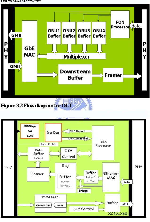
Up stream and down stream flow diagram for OLT and ONU are shown in figure3.2 and figure3.3. While up stream, each ONU send their data to OLT, OLT will identify the data from these 4 ONUs and put in different buffer, the header are then be removed. Finally central office gets the packets from users. While down stream, OLT add header in front of Ethernet packet, and send the packet to ONU. ONU removes header and check the MAC address. If the MAC address is right, ONU send the packet to user. The header for upstream and downstream are shown in figure3.4.
In the following sections, we focus on ONU part. The OLT part will be introduced clearly in Fang’s thesis.
P
H
Y
P
H
Y
GbE
MAC
Multiplexer
ONU1Buffer BufferONU2 BufferONU3 ONU4Buffer
Downstream
Buffer
Framer
PON Processor GMII GMII dataP
H
Y
P
H
Y
GbE
MAC
Multiplexer
ONU1Buffer BufferONU2 BufferONU3 ONU4Buffer
Downstream
Buffer
Framer
PON Processor GMII GMII dataP
H
Y
P
H
Y
GbE
MAC
Multiplexer
ONU1Buffer BufferONU2 BufferONU3 ONU4Buffer
Downstream
Buffer
Framer
PON Processor GMII GMII dataFigure 3.2 Flow diagram for OLT
Figure 3.4 Header of upstream packet(above) and downstream
packet(below)
3.2 PHY, Serdes and MII
3.2.1 Physical Layar
The lowest layer of the OSI Reference Model is layer 1, the physical layer; it is commonly abbreviated “PHY”. The physical layer is special compared to the other layers of the model, because it is the only one where data is physically moved across the network interface. All of the other layers perform useful functions to create messages to be sent, but they must all be transmitted down the protocol stack to the physical layer, where they are actually sent out over the network [19].
The Physical layer is responsible for the ultimate transmission of data over network communications media. It operates with data in the form of “bits” that are sent from the Physical layer of the sending (source) device and received at the Physical layer of the destination device [20].
In copper networks, the Physical Layer is responsible for defining specifications for electrical signals. In fiber optic networks, the Physical Layer is responsible for defining the characteristics of light signals [21].
3.2.2 Serdes
A SerDes transceiver (Serializer/Deserializer) takes byte or word wide data, converts it into a serial data stream and then transmits it over a differential media from point A to point B. This significantly reduces the number of signal paths and offers duplex data rates in the tens of gigabaud data rate [22]. The transmitter section is a serial-to-parallel converter, and the receiver section is a parallel-to-serial converter. Multiple SerDes interfaces are often housed in a single package.
SerDes chips facilitate the transmission of parallel data between two points over serial streams, reducing the number of data paths and thus the number of connecting PINs or wires required. Most SerDes devices are capable of full-duplex operation, meaning that data conversion can take place in both directions simultaneously. SerDes chips are used in Gigabit Ethernet systems, wireless network routers, fiber optic communications systems, and storage applications. Specifications and speeds vary depending on the needs of the user and on the application. Some SerDes devices are capable of operating at speeds in excess of 10 Gbps [23].
3.2.3 Medium Independent Interface
The MII is an optional set of electronics that provides a way to link the Ethernet medium access control functions in the network device with the Physical Layer Device (PHY) that sends signals onto the network medium [24]. The MII bus (standardized by IEEE 802.3u) is a generic bus that connects different types of PHYs to the same network controller (MAC). The network controller may interact with any
PHY using the same hardware interface, independent of the media the PHYs are connected to. The MII transfers data using 4-bit words (nibble) in each direction, clocked at 25 MHz to achieve 100 Mbit/s speed [25].
3.3 Up Stream
The main function in this part is to separate Ethernet packet into slots, each slot is 280 bytes. Since the maximum size of a packet on Ethernet is 1500 bytes, we may get 1~6 slots for one Ethernet packet. In the beginning of each slot, we also add header including 8 bytes Preamble, 1byte Delimiter, 1 byte ONU-ID and 2 bytes payload length. Finally slots are stored in buffer. We also count how many slots are stored in the buffer, then DBA will get this message. After DBA processor giving signal, one slot is been sent out. As we have mentioned before, data passing PHY here should be Media Independent Interface (MII), the data we receive are 4bits at 25 MHz data rate. Since the data we send out should be 16bits at 77.76 MHz data rate, that's also the work we have to do.
In order to accomplish all the functions above, I use ten modules to form the main up stream module. Each of them make a little change to data, and finally we get the data we want at the output of up stream module.
3.3.1 Ethernet MAC
The main work for Ethernet MAC is to count length of packets. After RX_DV pin being pulled up, 4 bits Ethernet packets are been sent into Ethernet MAC module. Then the data are sent out directly to buffer. In the same time, it also count the packet length after RX_DV is pulled up. When the packets come to its end, RX_DV pin is pulled down. Then we now know the packet length and module will send this message out to bufferl and buffer2. Notice here, we only consider the situation when packet length is even. Since the total output should be 16bits, we must form the data of the packet's end to be 16 bits. If
the data are not enough to form a 16bits number, we add 4'b0000 to make it possible. But now we only consider even packet length, so we can only get 16'h1234 or 16'h3400. 16'h represent for 16 bits hexadecimal number.
However, because buffers have limit capacity, they might be full if data are not sent out. To prevent buffers from being burst out, there’s a full pin for this module. When full pin is pulled up, the packets are then being dropped until full pin is pulled down.
Simulation results for Ethernet MAC are shown in figure3.5.
Figure 3.5 Simulation results for Ethernet MAC
3.3.2 Buffers
We can see in figure3.3 that in up stream modules, they include 5 buffer modules. These modules all contain memory of different size, three of them store data and two
of them store packet length. The memory we use here are dual-port block memory, we can see in figure3.6, they have independent two ports. So we make one port to be write-only, for we can set write enable pin to be always high. And so the other is read-only, for write enable pin is always low. Each of them is triggered by individual clock. Therefore, with these modules, we can change data rate and deal with data easily. These 5 buffer modules, they are Buffer0, Buffer1, Buffer2, Buffer3, Bufferl. All modules work almost the same way. When data are going to send, enable pin for write only part is pulled up, the data are then stored in memory according to priority. While positive edge clock, data are stored in one address, then the next address stored the next data. On the other hand, when we want to read the memory, enable pin for read only part is pulled up. By changing address in turn, the data are then read out.
Address of memory also tells us if the memory is full or empty. For example, we assume a dual-port block memory that it’s A port is write-only and B port is read-only. If ADDRA is less than ADDRB by one, maybe ADDRA = 10; ADDRB = 11. It means data in ADDRB might not be read. So now if we want to write more data, we have to write it in the space of ADDRA = 11, and that cover the old data which haven’t been read. That’s not what we want to see. So if ADDRA is less than ADDRB by one, we say the memory is full, the module will send a signal to tell. Likely, if ADDRB is less than ADDRA by one, we say the memory is empty because no more data could be read. Therefore the module also sends a signal to tell. Now, we always now when we can sends data, when we can read data.
Figure 3.6 Dual-port block memory
Buffer0
Buffer0 is the module after Ethernet MAC. This is the most important part of all. We set the input port for write-only part to be 4bits, for example, as in figure3.6, we let it be DINA[3:0]. Then the output port should be DOUTB, we let it be 16 bits. Then write-only part is triggered by CLKA, we set it to be 25MHz. On the other hand, we set CLKB to be 77.76MHz, which triggers read-only part. As a result, after data are sent in through PHY with 4 bits in 25MHz, we transform them to be 16 bits. After buffer0, the data are now transferring in 77.76MHz.
Simulation result for buffer0 is shown in figure3.7. The changes in bits number and data rate are clearly represented.
Figure 3.7 Simulation result for buffer0
Buffer
After we read data from buffer0, buffer stored the 16 bits data. There’s one problem that since the input bits and output bits for buffer0 are different, the priority of data are changed when we read them out. We now take hexadecimal number for example. At positive edge clock, the input for buffer0 is 4’h1, 4’h 2, 4’h 3, 4’h 4. 4’h represents for 4 bits hexadecimal number. When we read them out in 16 bits output, they will become 16’h4321, the priority are been changed. Therefore, one important job for buffer is to change them back. So we can get 16’h1234 and send into the input of memory.
Buffer2 and Bufferl
In Ethernet MAC, we count the length of Ethernet packets. After one packet is totally sent, its length is then stored in buffer2 and bufferl. The size of these two memories is just 32 bytes, for they only store packet length.
When buffer2 and bufferl store packet length, the modules are now not empty. Then the module bridge, which will be introduced later, starts to read data from buffer0 and send them to buffer. Length in bufferl let it know when it should stop. On the other hand, framer, which will also be introduced later, take data in buffer2 to count if that is going to be the last slot for a packet..
Buffer3
Buffer3 will be the most complicate module among these five buffers. Although it also stores data, communicate with DBA should be its main job.
Ethernet packets are been separated into several slots, each slot is 280 bytes. This work is done in framer. The slots are then stored in buffer3. DBA processor will give signal, one signal means one slot is going to send out. So, we let the module counts how many slots are stored in the memory. It communicates with DBA processor when one slot is totally sent in or be read out, so DBA can work and give signal to send the data out to OLT.
Figure 3.8 Simulation result for buffer3
3.3.3 Bridge
The output of buffer0 is directly connects to the input of buffer. Bridge plays the role to pull up enable pin, and count how long should the pin be pulled up. When bridge finds that a complete Ethernet packet is stored in buffer0, it pulls up the enable pin of read-only part of buffer0. It also reads packet length in bufferl. Since 2 bytes data are read at positive edge clock, we can count how long should the pin be pulled up easily.
3.3.4 Framer
We now come to the key part of the up stream module. Framer separates the Ethernet packet into slots, and also add header at the beginning of each slot.
Before framer read data from buffer, it sends header first. As we mentioned in 3.1, header include 8 bytes preamble, 1 byte delimiter, 1 byte ONU-ID and 2 bytes payload length. We set preamble to be 16'h5555, and delimiter to be 8'he2. Each ONU had its own ONU-ID, so this part is decided by extra input. Finally the payload length, in ordinary it is always 16'h010C, which means this payload is 280 bytes. But we also read the packet length in buffer2, therefore we can count which slot is the last slot for a packet. This time, the payload length of the header may not be 16'h010C, because the remainders probably less than 280 bytes. So we payload length is the remainder's length, and also the first pin of this 2 bytes is been pulled up. The data might be like 16'h8XXX now, OLT will know that it is the last part of a packet through the header like this. Now, the header for one Ethernet packet is ready.
After 12 bytes header is been sent, framer reads data from buffer and send them out to buffer3. Counter also starts to count. Since each slot should be 280 bytes, when there are 268 bytes data been sent, again framer gives header. The process is repeated until counter is larger than payload length. It means this Ethernet packet is been sent completely. Now, we still have to make it a 280 bytes slot. So if it hasn’t been 280 bytes yet, we give a idle signal 16’hAAAA to make it complete.
Simulation result for framer is shown in figure3.9. It is clear that Ethernet packet are now been separated into slots. We can also notice that the in the last slot, the payload length of the header is 16'h8XXX.
Figure 3.9 Simulation result for framer
3.3.5 DBAcontrol
Finally, we now control the output of the up stream module. When DBAcontrol module get signal from DBA processor, it pull up the enable pin of the read-only part of buffer3. After 280 clock, there should be 280 bytes data been sent, the pin is then pull down.
Therefore, we can get one slot with header after DBA processor gives signal in the output of the module.
3.3.6 Simulation Result
The simulation result after post-place & route can be seen in figure3.11, figure3.12 and figure3.13. The RTL scheme of the total module is also seen in figure3.10.
Figure 3.11 Simulation result for full upstream module after
post-place & route (input)
Figure 3.12 Simulation result for full upstream module after
post-place & route (header of output)
Figure 3.13 Simulation result for full upstream module after
post-place & route (end of packet)
3.4 Down Stream
Unlike we have done in up stream module, the main function in this part is to remove header of data, which are added in OLT. Then we pull up TX_EN signal and send data to PHY. Likely, as we have mentioned before, the data should be Media Independent Interface (MII), therefore the data we send out should be 4bits at 25 MHz data rate. Since the data ONU received are 16bits at 77.76 MHz data rate, we also have to make a change here.
In order to accomplish all the functions above, I use four modules to form the main down stream module. Each of them make a little change to data, and finally we get the data we want at the output of down stream module.
3.4.1 PON MAC
The first part in ONU down stream is passive optical network media access control (PON MAC). The function of this part is to remove header of data. First of all, we have to find where the data begin. Since network is global, we might receive data which are not we expect, such as noise, or other ONU’s data. So if we want to find the beginning of the data, finding out header is our solution. We have seen in 3.1 that header in down stream data include 3 bytes PSYNC, 1 byte Delimiter and 2bytes Packet Length. In these 6bytes header, the most important is delimiter. So when we find delimiter, we could get the beginning of the data. However, during the transporting of data, PSYNC might be lost, that means delimiter might be shift, probably 1 bit, or even 18bits, for the PSYNC signals are all lost. So now we separate PON MAC into two parts, one is corrector, the other is main PON MAC.
Corrector
We may see that after 3 bytes PSYNC, there comes 1 byte delimiter. That means that if no data is lost, for data received in 2 bytes, we can always find delimiter after 1 byte PSYNC. If delimiter is shifted, we must do something or we might lose the whole data. So corrector is the module which solves this problem. No matter how many bits delimiter is shifted, it shifts back after passing this module. So we can get the beginning of data as 1 byte delimiter after 1 byte PSYNC. Then the output of this module is connected to the input of the next – main PON MAC.
The simulation results for corrector are shown in figure3.14. we could see that no matter how the delimiter is shifted, we will always get a 16’h55E2. That means we can always shift it back.
Main PON MAC
In this module we remove header of the data. But first of all, since data are global, we have to check if the data belong to this ONU or not. We have seen in chapter 2 that Ethernet packet include source address and destination address. So, after checking delimiter, we also check source address here. If data match the condition, the module records the packet length and sends data out; if not, the module drops the packet and waits the next delimiter to come. The output is then connected to the next part – BufferO.
Simulation results for main PON MAC are shown in figure3.15.
3.4.2 BufferO
Just as all the buffers work in upstream, buffero stores data. The only difference is that the input data are 16 bits in 77.76 MHz, but the output data are 4bits in 25MHz. That is because we connect the output to PHY directly. Now, nearly all the works in downstream module are done. The last part should be the module which controls the output stream – Outcontrol.
Simulation results for bufferO are shown in figure3.16 and figure3.17.
Figure 3.16 Simulation results for bufferO. Above : input situation
Below : MAC address is shown
Figure 3.17 Simulation results for BufferO (output situation)
3.4.3 Outcontrol
Just like RX_DV is pulled up when PHY send data to FPGA in upstream steps, here we also pull up TX_EN when FPGA send data to PHY. In this module, it also controls the enable pin of buffero, we can see how it works in figure3.18. If data are recognized in main PON MAC, packet length is recorded and sent to outcontrol module. Notice the red circle, the length is been recorded. If another packet is coming, the lengths are then been added. Now we know how many bytes there in the buffer, so the module pulls up TX_EN pin and send the data out. All the works in down stream steps are now done.
Figure 3.18 Simulation results for outcontrol
3.4.4 Simulation Result
The RTL scheme is shown in figure3.19.
The simulation result after post-place & route can be seen in figure3.20, we can see that header is removed, and after TX_EN pin is pulled up, the output are then of 4 bits in 25 MHz.
Figure 3.19 RTL scheme of the full downstream module
Figure 3.20 Simulation result for full downstream module after
post-place & route
CHAPTER 4
O
NB
OARDT
ESTING4.1 Field Programmable Gate Array (FPGA)
A field-programmable gate array is a semiconductor device containing programmable logic components called "logic blocks", and programmable interconnects. Logic blocks can be programmed to perform the function of basic logic gates such as AND, and XOR, or more complex combinational functions such as decoders or simple mathematical functions. In most FPGAs, the logic blocks also include memory elements, which may be simple flip-flops or more complete blocks of memories [26].
Field Programmable means that the FPGA's function is defined by a user's program rather than by the manufacturer of the device. A typical integrated circuit performs a particular function defined at the time of manufacture. In contrast, the FPGA's function is defined by a program written by someone other than the device manufacturer. Depending on the particular device, the program is either 'burned' in permanently or semi-permanently as part of a board assembly process, or is loaded from an external memory each time the device is powered up. This user programmability gives the user access to complex integrated designs without the high engineering costs associated with application specific integrated circuits [27].
In our experiment, we use a Xilinx Virtex-4 FPGA. Table4.1 shows the specification of it. The FPGA is just one part of our board, but it’s the most important. The verilog module we write in chapter 3 is loaded into the FPGA, and works the way we want.
1490nm/1310nm/1550nm Dn/Up/Ctrl PON Wavelength ONU Spec. 2.5G/1.25G/155M Dn/Up/Ctrl PON Rate 1 PON 160 x 16Kb (~320KB) Internal BKRAM Size
1.5K Packet MTU 1xGbE Down link Data Interface FPGA Items 17Mb ROM Size FF688-11 XC4VLX60 Spec. Table 4.1 1490nm/1310nm/1550nm Dn/Up/Ctrl PON Wavelength ONU Spec. 2.5G/1.25G/155M Dn/Up/Ctrl PON Rate 1 PON 160 x 16Kb (~320KB) Internal BKRAM Size
1.5K Packet MTU 1xGbE Down link Data Interface FPGA Items 17Mb ROM Size FF688-11 XC4VLX60 Spec. 1490nm/1310nm/1550nm Dn/Up/Ctrl PON Wavelength ONU Spec. 2.5G/1.25G/155M Dn/Up/Ctrl PON Rate 1 PON 160 x 16Kb (~320KB) Internal BKRAM Size
1.5K Packet MTU 1xGbE Down link Data Interface FPGA Items 17Mb ROM Size FF688-11 XC4VLX60 Spec. Table 4.1
4.2 ONU Board
Figure4.1 shows the board of ONU. The component which is been circled is our Virtex4 FPGA. We drive the board in about 0.4mA (12V). When we have simulated, synthesized our design, we generate a bit file, and download it on to FPGA using a Xilinx iMPACT. The board is now working according to the functions we design. To assure that it is really working, we can give input data and get output data through the test pins. We can see the test pins are in the bottom of figure4.1.
The board and computer are connected using a network line. We use EthView to generate Ethernet packets and send into the board. The serial data are converted to parallel data in the physical layer (PHY). The data are then been sent into FPGA. We use Logic Analyzer (LA) to get the output in the test pins. Finally, we can show that our FPGA does work or not.
4.3 Testing Result
The target of this design is to connect ONU and OLT, and transfer data between central office and users. If we want to see the signals in the output, we assign the output pins to the test pins of the board. After that, we use a Logic Analyzer, which displays signals in a digital circuit that are too fast to be observed by a human being and presents it to a user so that the user can more easily check correct operation of the digital system.
The equipment we use is shown in figure4.2. We can then get the output data by connecting the probes to the test pins. We can see how they are connected in figure4.3. Comparing the input data and the output data, we can see if our design works.
Figure 4.2 Logic Analyzer
4.3.1 Up Stream
In upstream process, we use EthView to collect packets on the network. After that we connect the board and computer using a network line. EthView can continuously send the packets we have picked. As we can see in figure4.4, we send the selected packets to the board. The data of the packets are also shown in the figure. Logic Analyzer now shows the output in the screen. We can see the results in figure4.5 to figure 4.9.
Figure4.5 shows that our module has successfully separated the packet into slots. Figure4.6 and Figure4.7 show that the header is added in front of the packet, the data also match the data we send in. Figure4.8 and Figure4.9 show that at the end of the packet, we add idle signal 16’hAAAA. After that, the next packet is started.
Figure 4.5 Packet has been separated into slots
Figure 4.7 Data of the slot
Figure 4.9 Next packet comes in
In figure 4.10 we send a short packet of 60 bytes only. We can see that only one slot is presented.
4.3.2 Down Stream
In down stream process, the data it receives should be from OLT. If we want to test ONU part only, we should generate the packets by our own. So we again write a module to generate Ethernet packets and send into the input of the first module of the down stream modules.
Figure4.11 shows the data we send in, we set the MAC address to be 16’h0001, 16’h0003, 16’h0007. In figure4.12, we can see clearly that the header has been removed, the data start at MAC address. We can also see our packet in figure4.13, the data perfectly match the data we send in.
Therefore, we are sure that our module for down stream does work in the ONU board. Thus we can now try to connect OLT and ONU. It’s our future work.
Figure 4.12 MAC address of output data
CHAPTER 5
C
ONCLUSION5.1 DHPON
Passive Optical Networks are the basis of FTTx access applications. Within the access network, there’s no active components, therefore require little maintenance and have a high MTBF (Mean Time Between Failures). PON also Provides higher bandwidth due to deeper fiber penetration, and it has Longer distances between central offices and customer premises. PON is Easy to upgrade to higher bit rates or additional wavelengths, and Share their costs of fiber and the equipment at the central office among multiple customers
However, PON also suffers from serious problem that packet delay might occur due to the long round trip time. Some bandwidth might also be wasted in this situation. Therefore a distributed-control hybrid passive optical network is introduced. In this architecture, it contains both TDM and WDM system. Distributed-control dynamic bandwidth allocation is worked close to a few ONU. A shorter RTT means the packet delay problem is solved. The queue sizes are updated quickly because control massage and data transmitting are using different wavelength. Now, we have theoretically known that DHPON does have some advantage compare to the traditional PON.
5.2 Future work
The design for Optical Network Unit (ONU) is successfully worked. In the upstream part, after user sending packet to ONU, our module divides the packet to some 280 bytes slots. Each slot contains 12 bytes header including 8 bytes Preamble, 1 byte delimiter, 1 byte ONU-ID and 2 bytes payload length. In the downstream part, ONU
receive packets from OLT. Our module then remove header of the packet and check the MAC address. If the MAC address matches the ONU, the packet is then send to user. On the other hand, the design for Optical Line Terminal (OLT) is also done by Chien-Ho Fang.
Therefore, we have successfully set up an OLT and ONU that send and receive Ethernet packets. To complete the whole architecture, we now start to connect OLT and ONU together. We’ll check both upstream and downstream flow and compare the packet that sent in and sent out. After that we’ll work the distributed-control DBA among several ONUs. Finally, we’ll set up a real distributed-control hybrid passive optical network.
In the end, we will prove that our DHPON will work in the real world and how it is superior to the traditional PON.
R
EFERENCE[1]. Amitabha Banerjee, Youngil Park, Frederick Clarke, Huan Song, Sunhee Yang, Glen Kramer, Kwangjoon Kim and Biswanath Mukherjee “Wavelength-division-multiplexed passive optical network (WDM-PON) technologies for broadband access: a review” Journal of Optical Networking, vol. 4, no. 11, pp. 737-758, November 2005.
[2]. G. Kramer, B. Mukherjee, and G. Pesavento, “Ethernet PON (EPON): Design and Analysis of an Optical Access Network,”Photonic Network Comm., vol. 3, no. 3, pp. 307-319, July 2001.
[3]. Michael P. McGarry, Arizona State UniversityMartin Maier, Centre Tecnològic de Telecomunicacions de Catalunya Martin Reisslein, Arizona State University, “Ethernet PONs: a survey of dynamic bandwidth allocation (DBA) algorithms,” IEEE Commun. Mag., vol. 42, no. 8, pp. S8–S15, Aug. 2004.
[4]. G. Pesavento and M. Kelsey, “PONs for the Broadband Local Loop,” Lightwave, vol. 16, no. 10, pp. 68-74, Sept. 1999.
[5]. B. Lund, “PON Architecture ‘Futureproofs’ FTTH,” Lightwave, vol. 16, no. 10, pp. 104-107, Sept. 1999.
[6]. “Ethernet Passive Optical Network(EPON) A Tutorial,” Metro Ethernet Forum 2005
[7]. Soo-Jin Park, Chang-Hee Lee, Ki-Tae Jeong, Hyung-Jin Park, Jeong-Gyun Ahn, and Kil-Ho Song “Fiber-to-the-Home Services Based on Wavelength-Division-Multiplexing Passive Optical Network,” J. Lightwave Technol. 22, pp. 2582–2590 (2004).
[8]. DJ. Shin, D.K. Jung, H.S. Shin, J.W. Kwon, Seongtaek Hwang,Y.J. Oh, and C.S. Shim “Hybrid WDM/TDM-PON for 128 subscribers using λ-selection-free transmitters,” PostDeadline paper PDP4, OFC'2004.
[9]. Novera optics white paper “WDM-PON for the Access Network“ http://www.noveraoptics.com/downloads/Novera_WP_WDM-PO N_062906.pdf
[10]. G. Kramer, B. Mukherjee, and G. Pesavento, “Ethernet PON (EPON): Design and Analysis of an Optical Access Network,” Photonic Network Comm., vol. 3, no. 3, pp. 307-319, July 2001.
[11]. D. Nikolova, B. Van Houdt, and C. Blondia “Dynamic bandwidth allocation algorithms for Ethernet Passive Optical Networks with threshold reporting.” [12]. G. Kramer, B. Mukherjee, and G. Pessavento, “Interleaved Polling with
Adaptive Cycle Time (IPACT): a dynamic bandwidth distribution scheme in an Optical access network”, Photonic Network Comm. 4, pp. 89–107, Jan 2002.
[13]. Dawid Nowak, under the supervision of Dr. John Murphy “Dynamic Bandwidth Allocation Algorithms for Differentiated Services enabled Ethernet Passive Optical Networks with Centralized Admission Control,” A thesis submitted in March 2005 for the degree of Doctor of Philosophy in the School of Electronic Engineering, Dublin City University.
http://www.eeng.dcu.ie/~pel/graduates/DawidNovak-PhD-thesis.pdf
[14]. http://en.wikipedia.org/wiki/Hardware_description_language J. Mermet (editor): Fundamentals and Standards in Hardware Description Languages (Springer Verlag, 1993)
[16]. http://www.xilinx.com/products/design_tools/logic_design/design_entry/proj nav.htm
[17]. http://www.synplicity.com/products/synplifypro/
[18]. Peter Hornyack, Milo Martin, CSE 372 (Spring 2007): Digital Systems Organization and Design Lab, “Xilinx ModelSim Simulation Tutorial,” [19]. The TCP/IP Guide “Physical Layer(Layer 1)”
http://www.tcpipguide.com/free/t_PhysicalLayerLayer1.htm
[20]. http://compnetworking.about.com/od/basicnetworkingconcepts/l/blbasics_os i1.htm
[21]. TECH FAQ, “What is the physical layer,” http://www.tech-faq.com/physical-layer.shtml
[22]. Freescale semiconductor, “Gigabit Serdes Tranceivers,”
http://www.freescale.com/webapp/sps/site/homepage.jsp?nodeId=01435940 582350
[23]. http://searchstorage.techtarget.com/sDefinition/0,290660,sid5_gci1006456,0 0.html
[24]. Components Used For a 100-Mbps Connection, “Medium Independent Interface,” http://www.ethermanage.com/ethernet/100quickref/ch9qr_7.html [25]. http://en.wikipedia.org/wiki/Media_Independent_Interface
[26]. http://en.wikipedia.org/wiki/FPGA