行政院國家科學委員會專題研究計畫 期中進度報告
總計畫
計畫類別: 整合型計畫 計畫編號: NSC91-2120-E-009-002- 執行期間: 91 年 08 月 01 日至 92 年 07 月 31 日 執行單位: 國立交通大學電子工程學系 計畫主持人: 李建平 共同主持人: 孫允武,孫建文 報告類型: 精簡報告 處理方式: 本計畫可公開查詢中 華 民 國 92 年 7 月 1 日
行政院國家科學委員會專題研究計畫期中報告
半導體量子結構與量子元件前瞻性研究(2/3)
總計畫
計畫編號:NSC91-2120-E009-002
執行期限:91 年 8 月 1 日至 92 年 7 月 31 日
主持人:李建平 國立交通大學電子工程系
共同主持人:孫建文 國立東華大學物理系
孫允武 國立中興大學物理系
中文摘要 此報告為總結本實驗室在本年度於「半導體量子結構與量子元件前瞻性研 究」專題計畫的研究成果。在化合物半導體量子結構之成長與探討中,我們利用 分子束磊晶系統,探討了線狀量子結構的長晶條件與物理特性,且初步得到量子 環與量子點分子結構。在化合物半導體量子奈米元件之製作與高頻及磁傳輸特性 研究中,利用設計的脈衝式射頻及微波訊號的高解析度第二類鎖相迴圈偵測系 統,測試了二維電子系統樣品,測量頻率由幾百 MHz 到超過 7GHz,觀測到傳輸 訊號振幅與相位的振盪,也成功的利用電子微影術製作出中心頻率超過 3GHz 的 表面波延遲線及量子通道元件。在化合物半導體量子結構之光學性與與其載子動 力學之探討中,我們架設了時域解析光激發光實驗系統來觀察超快載子動力行 為,利用此系統與結合理論計算探討了量子結構內的熱電子散射行為。 關鍵詞:化合物半導體、分子束磊晶系統、量子環、量子點、鎖相迴圈、電子微 影術、二維電子系統、表面波、量子通道、時域解析光激發光、載子動力行為。3
I. Abstract
This reports summarized the results of “Semiconductor quantum structure and quantum device” in this year. In the growth and investigation of compound semiconductor quantum structure, we used molecular beam epitaxy (MBE) system to obtain the wire-like quantum structure, and investigate their physical properties. In addition, we have also successfully fabricated quantum rings and quantum dot molecule-like nanostructures via MBE. In the studying of the high-frequency and magneto transport properties of quantum nanoelectronic devices, we used our homemade phase-lock-loop (PLL) detection system for pulsed microwave signals to observe the magneto quantum oscillations in two-dimensional electron systems (2DES) at temperature of 0.3K. The frequency ranges from few hundred MHz to above 7 GHz. The real part and imaginary part of the conductivity can be derived from our data. We have also used e-beam lithography process to fabricate high-frequency surface-acoustic-wave (SAW) transducers with center frequency exceeding 3GHz and quantum channel devices. In the investigation of optical properties of quantum structures and studies of carrier dynamics, we have purchased necessary equipments for the construction of a time-resolved luminescence up-conversion system for observing the ultrafast carrier dynamics. With the system and combining the theory studying, we investigated the ultrafast carrier dynamics in the quantum structure system.
Keywords: Compound semiconductor, Molecular beam epitaxy system (MBE),
quantum rings, quantum dots, phase-lock-loop (PLL), e-beam lithography, two-dimensional electron systems (2DES), surface-acoustic-wave (SAW), quantum channel, time-resolved luminescence up-conversion system, carrier dynamics.
Part I: The growth, physical property, and device application of semiconductor quantum structure
Varian GEN Ⅱ MBE system was used to epitaxy the required structure on (100) InP substrate. InGaAs or InAlAs layer, lattice matched to InP, was grown as the matrix material for the nanostructures.
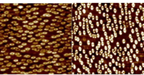
Fig.1 are the AFM pictures of InAs and GaAs wire-like structure on InGaAs matrix. Because InAs has smaller band gap than InGaAs and GaAs has larger one than InGaAs, InAs wire-like structure forms QWrs and GaAs wire-like structure forms anti QWrs in InGaAs matrix.
Fig.1.(a)The AFM picture of InAs wire-like quantum structure in InGaAs matrix. (b)The AFM picture of GaAs wire-like quantum structure in InGaAs matrix.
Fig.2(a), Fig.2(c), and Fig.2(e) were cross-sectional TEM pictures of [110] facets and revealed that all InAs or GaAs structures had dot-like patterns. However, Fig.2(a), Fig.2(c), and Fig.2(e), the [110] cross-sectional TEM pictures, showed the InAs or GaAs structure had more uniform wire-like patterns. So InAs and GaAs both formed wire-like structures, which extended along [110] direction. Moreover, the stacked wire-like quantum structure in InGaAs matrix were both vertically aligned, however, the stacked InAs QWrs in InAlAs were spatial anti-correlated. The distinct adatom diffusion coefficient and different reactivity of step edge along [110] and [110] direction should be the main factors for wire-like structure formation. Phase separation was also observed for these wire-like quantum structures. The phase separation should be caused by sureface energy and the strain energy. And the different shape of phase separation makes wire-like structures in InGaAs be spatial correlated and makes wire-like structure in InAlAs be spatial anti-correlated.
(a) (b)
(c) (d)
(e) (f)
Fig.2.(a)(b)InAs quantum structure in InGaAs. (c)(d)GaAs quantum structure in InGaAs. (e)(f)InAs quantum structure in InAlAs.
5
We also investigated the carrier transport property of the GaAs anti-wires using an InGaAs/InAlAs 2DEG structure. The GaAs anti QWrs were embedded below the 2DEG interface, see Fig.3. For comparison, another sample with the same structure but without the wires was also grown. For the sample without GaAs anti QWrs, isotropic 2DEG mobility was observed. However, for the samples with anti QWrs, clear difference between the devices perpendicular and parallel to the wires was observed, see Fig.4. This anisotropy can be explained by the difference in the electron’s scattering cross section along the two different directions because of the presence of the wires near the conduction channel.
Fig.3.The structure of the InGaAs/InAlAs modulation doped structure used in this study.
Fig.4. The temperature dependent mobility for the devices with GaAs anti QWrs.
Fig.5(a) is the AFM picture of surface morphology of our preliminary quantum ring. The way to obtain quantum ring is to cap GaAs layer, of which the thickness is smaller than the height of QDs, on QDs and than annealing the wafer. Fig.5(b) is the AFM picture of molecular-like quantum structure. The epitaxy recipe is similar to quantum ring but change the epitaxy condition.
Fig.5.(a)The AFM picture of quantum ring. (b)The AFM picture of molecular-like quantum structure.
PART II: Fabrication, and high-frequency and magneto transport properties of quantum nanoelectronic devices
The high-frequency magnetotransport coefficients of a two-dimensional electron system (2DES) can be detected by type-II phase lock loop (PLL) for pulsed RF signals. A meandering coplanar waveguide (CPW) (Fig.6) is patterned on the surface of a substrate, containing a high-mobility 2DES in a modulation-doped GaAs/AlGaAs heterostructure.
Fig. 6 The pattern of the meandering coplanar waveguide. The dark part is the metal.
The xx can be obtained from the attenuated signal amplitude A traveling through
the CPW via
1 0 ln } Re{ Z A d xx (1) 0 } Im{ Z d s xx (2)where s is the change in the imaginary part of the propagation constant of the CPW
and is given by –(L/)(2f/L). L denotes the total length of the semirigid cable
connecting the sample and the PLL system and L is the velocity of the signal in the
cable.
The slope of each curve S in Fig.7 should be proportional to the localization length according to
(3)
For S=1 S/GHz, is 4.5 m which is much larger than the magnetic length at this B.
0 3 2 )} ( Re{ xx
7
Fig. 7(c) gives a broad minimum near B=8.8T where we set as the center of the =1 plateau (B1). By fitting the high-field and the low-field side of the curve separately to
S=a|B-B1|b, b=2.220.06 and 1.960.06 for each side. Figure 7(d) shows a log-log
plot for S vs. |B-B1| and the slope gives b. This allows us to get the magnetic field
dependence of localization length near the center of the plateau:
b b B B 1 1 (4)
where we have used B. To our knowledge no published theoretical work predicts the power relation like Eq. 8 near the plateau center. The =2 data yield b=2.210.02 and 2.050.07, and the =3 data yield b=1.720.05 and 1.860.07 for high- and
low-field sides respectively. The =3 plateau has a slightly different exponent from the
=1 and 2 plateau, which may relate to the incomplete development of the plateau at
this temperature.
(a) (b)
(c)
Fig. 7 (a) and (b) show Re{xx} vs. f in the =1 plateau region. The slope S vs. B is shown in (c).
(d) shows the log-log plot of S vs. |B-B1| where B1=8.8T.
(a) 0.0 0.5 1.0 1.5 2.0 2.5 3.0 0.0 0.5 1.0 1.5 2.0 2.5 3.0 3.5 4.0 B=8.0T R e{ }xx ( S) Frequency (GHz) B=8.1T B=8.2T B=8.3T B=8.4T B=8.5T B=8.6T B=8.7T B=8.8T 0.0 0.5 1.0 1.5 2.0 2.5 3.0 0.0 0.5 1.0 1.5 2.0 B=8.8T R e{ }xx ( S) Frequency (GHz) B=8.9T B=9.0T B=9.1T B=9.2T B=9.3T B=9.4T B=9.5T B=9.6T B=9.7T B=9.8T 8.0 8.5 9.0 9.5 10.0 0.0 0.2 0.4 0.6 0.8 1.0 1.2 S ( S/G H z) B (T) 0.1 1 10-3 10-2 10-1 100 =1 B0=8.8T B>B0 B<B0 S ( S/G H z ) B (T) 0.0 0.1 0.2 0.3 0.4 0.5 0.6 -0.15 -0.10 -0.05 0.00 0.05 0.10 0.59GHz 0.96GHz 2.12GHz 2.92GHz Im { xx } (e 2 /h ) Re{xx} (e2/h) 0.05 0.10 0.15 } ( e 2 /h )
(b)
Fig. 8 Im{xx} vs. Re{xx} for transition from 1 to 2 (a) and 2 to (3) for selected f. The arrow for
each curve shows the direction of increasing .
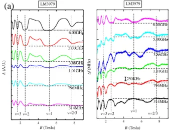
Fig.9 shows the amplitude and the frequency dependence on B. This set of data shows clearly the feature near 2/3 FQHE state. This sample was grown by the NCTU group.
(a)
Fig. 9 (a) The amplitude and (b) the frequency deviation f (phase) vs magnetic fields for frequency up to 6 GHz. Each curve is offset for clarity.
We further improved our pulsed PLL detecting system by replacing the power detection part by a homodyne design, which includes a 90-degree hybrid to get another reference signal having a 90° phase difference from the original reference signal, a mixer, and the same sample-and-hold and averaging circuits. The resolution is better than 0.0002° at the average input power less than –120dBm (test at 5GHz), which is much better than a commercial vector analyzer (0.01°). After the arrival of
2 4 6 8 =2/3 =3=2 =1 6.00GHz 5.00GHz 3.86GHz 1.01GHz 796MHz 314MHz LM3979 A ( A .U .) B (Tesla) 2 4 6 8 250KHz =2/3 =3=2 =1 6.00GHz 5.00GHz 3.86GHz 1.01GHz 796MHz 314MHz LM3979 f (M H z) B (Tesla)
9
the high-frequency components, our PLL system can operate up to 18 GHz so far. Fig.10 show the SEM micrographs of one set of the Ti/Au electrodes of the IDT transducer pair. The width of the electrode fingers is about 200nm for generating a SAW of wavelength 800nm. Since the substrate is an insulator (GaAs or LiNO3), it
is very difficult to write small patterns on it due to the charging effect. We have developed a process including evaporating a Ge conducting layer before spinning on PMMA, and removing with RIE after metal lift-off.
We also use e-beam lithography system to fabricate quantum channels that can be placed between the SAW IDTs so that acoustoelectric effect can be studied. A pair of split gates can control the effective width of the channel. We etched away the 2DEG under the split gates before depositing the metal to obtain more strong confinement of the carriers in the channel. The operating temperature for this quantum device may be higher than that without etching process. Figure 11 (a) and (b) shows the device under a optical microscope and a SEM respectively.
Fig.10
(a) (b)
Fig.11(a) (b)
We combined a high-frequency signal synthesizer (100k~40GHz) and a spectrum analyzer (9k~26.5GHz) to form a pulsed-gated-power measurement system with fully automatic PC controlling program. This system complements the shortcoming of our high-resolution PLL detection system which is lack of the absolute accuracy for the amplitude detection. We utilize the gated mode of the spectrum analyzer triggered by the pulse signal from the built-in pulse generator of the signal synthesizer. The spectrum analyzer sets the signal-selection timing gate. The resolution can reach the
limit of the spectrum analyzer. Figure 12 shows the block diagram of this system. The control program is written in Labview.
Fig.12
PART III : optical properties of quantum structures and studies of carrier dynamics and gain dynamics in quantum dot laser systems
We have purchased necessary equipments for the construction of a time-resolved luminescence up-conversion system with the matching funds from National Dong Hwa University. Combination of this system and a monochromator allows us to measure the ultrafast carrier dynamics in the QW and QD system with the time resolution of about one hundred femtosecond.
We have studied the inter-subband and intra-subband scatterings of hot electrons in quantum wells using the hot electron-neutral acceptor luminescence technique. We have observed direct evidences of the emission of confined optical phonons by hot electrons excited slightly above the n=2 subband in GaAs/Al0.37Ga0.63As quantum
wells. Scattering rates of photoexcited electrons via inter- and intra-subband LO phonon emission were calculated based on the dielectric continuum model (DCM). We found that, for wide wells with the given Al composition, both the calculated and experimental results suggest that the scatterings of the electrons are dominated by the confined LO phonon mode.
About the inter-subband scattering of electrons in GaAs/A0.37Ga0.63As quantum
well, in our calculations, the types of phonons that interact with electrons in the wells are determined based on the DCM. In contrast to the earlier results in narrower
11
quantum wells, we find that the inter- and intra-suband transitions are both dominated by the confined LO phonons for wide GaAs/AlGaAs well and the inter-subband scattering rates are faster for electron confined in L valleys than those in the gamma valley. Our results are in good agreement with recent experimental results.
We investigate experimentally the scattering mechanisms between the electrons and holes and the influence of an electron and hole distribution near k=0 on the femtosecond carrier thermalization process in modulation doped GaAs/AlGaAs QW. In contrast to the earlier report by Knox et al., we find that the presence of a cool thernalized distribution at zone center does not affect the scattering rate significant. We have compares the scattering rate of hot electron in the undoped and modulation doped QW samples. The time-resolved photoluminescence spectra are shown in figure 13.
Fig 13
We dealt with the time evolution for the building up of the Coulomb screening in bulk GaAs and quantum wells. The behaviors for the shielding strength and the screening growth duration in the two different dimensional systems are studied. In contrast to the earlier results, we find the shielding strength in a quantum well is stronger than in a bulk. Nevertheless, a nonequilibrium carrier distribution still thermalizes in a quantum well faster than in a bulk due to the dominance of a stronger bare Coulomb interaction. Regarding to the screening growth duration, a slower screening development in a quantum well is expected because two-dimensional charges generally take longer time to form a plasma vibration than three-dimensional charges.
Generalized Kadanoff-Baym Equation (GKBE) with GKBA (ansatz) is used to study the quantum screening kinetics. Two and three dimensions cases are strictly
treated. Because the divergent CCS rate at the vanishing wave vector is handled in GKBE, we can compare the bare Coulomb interaction between a bulk and a quantum well from the evolution of nonequilibrium carrier distribution. As time evolves, the shielding potential gradually builds up and screens the carrier-carrier interaction. The dependences of the screening behaviors on the background and photo-excitedcarrier densities are also obtained and are compared to the earlier results. The energy-nonconservation and the memory effect gradually evanesce due to the sufficient CCS and the screening kinetic theory can be simplified with the dynamically screening Boltzmann equation.
Publication
[1] S. D. Lin, C. P. Lee, W. H. Hsieh, and Y. W. Suen, “Self-assembled GaAs antiwires in In0.53Ga0.47As
matrix on (100) InP substrates”, Appl. Phys. Lett., Vol. 81(16), p.3007, Oct. 2002.
[2] Z. C. Lin, S. D. Lin, and C. P. Lee, “Growth of stacked InAs/GaAs quantum structures in InAlAs/InGaAs matrix on (100) InP substrate”, LDSD Proc. (2002), Ceara, Brazil.
[3] C.-C. Li, L. W. Engel, D. Shahar, D. C. Tsui, and M. Shayegan, Phys. Rev. Lett. 79, 1353 (1997). [4]D. G. Ployakov and B. I. Shklovskii, Phys. Rev. B 48, 11 167 (1993); Phys. Rev. Lett. 70, 3796 (1993).
[5]B.C. Lee, S.D. Lin, C.P. Lee, H.M. Lee, J.C. Wu, and K.W. Sun, “Selective growth of single quantum dots using strain engineering”, Applied Physics Letters 80, pp.326-328 (2002).
[6]H.C. Lee, K.W. Sun and C.P. Lee, “Structure effects on electron-optical phonon interaction in GaAs/AlxGa1-xAs quantum wells”, Journal of Applied Physics 92, pp. 268-273 (2002).
[7]K.W. Sun, C.L. Huang, G.B. Huang and H.C. Lee, “Inter- and intra-subband relaxation of hot electrons in GaAs/AlGaAs Quantum wells”, Solid State Communications Vol. 126, pp. 519-522 (2003) [8]H.C. Lee and K.W. Sun, “Calculations of the Inter-subband scattering rates of electrons in GaAs/AlGaAs quantum wells”, Microelectronics Journal Vol. 34/5-8, pp. 671-673 (2003)
[9]H.C. Lee, K.W. Sun, and C.P. Lee, “Structure effects on electron-optical phonon interaction in GaAs/AlxGa1-xAs and strained InxGa1-xAs/GaAs quantum wells”, 10th Internation Symposium on
Nanostructures: Physics and Technology, 17-21 June, 2002, St. Petersburg, Russia
[10]H.C. Lee, C.L. Huang, G.B. Huang and H.C. Lee and K.W. Sun, “Inter- and intra-subband relaxation of hot electrons in GaAs/AlGaAs Quantum wells”, The Fourth International Conference on Low Dimensional Structures and Devices (LDSD2002), 8-13 December, 2002, St. Fortaleza, Brazil. [11]H.C. Lee, K.W. Sun and C.P. Lee, “ The Comparison of the Screening Behavior between Bulk GaAs and Quantum Wells in Quantum Kinetic Regime”, the 13th International Conference on Nonequilibrium Carrier Dynamics in Semiconductors (HCIS-13), July 28-August 1, Modena, Italy