國 立 交 通 大 學
材料科學與工程學系
博 士 論 文
多孔性氧化鋁薄膜之發光性質研究及其在光學上應用
A Study on Photoluminescence Properties of Porous Alumina
Membranes and Their Optical Application
研究生: 陳 蓉 萱
指導教授: 朝 春 光 博士
劉 增 豐 博士
多孔性氧化鋁薄膜之發光性質研究及其在光學上應用
A Study on Photoluminescence Properties of Porous Alumina
Membranes and Their Optical Application
研究生: 陳蓉萱 Student: Jung-Hsuan Chen
指導教授: 朝春光博士 Advisor: Dr. Chuen-Guang Chao
劉增豐博士 Dr. Tzeng-Feng Liu
國立交通大學
材料科學與工程學系
博士論文
A Dissertation
Submitted to Department of Materials Science and Engineering
College of Engineering
National Chiao Tung University
in partial Fulfillment of the Requirements
for the Degree of
Doctor of Philosophy
in
Materials Science and Engineering
June 2008
多孔性氧化鋁薄膜之發光性質研究及其在光學上應用
研究生:陳蓉萱 指導教授:朝春光 博士
劉增豐 博士
國立交通大學
材料科學與工程學系博士班
摘 要
本研究的目的是以純鋁的陽極處理法製備多孔性氧化鋁薄膜,並
且研究其光激發光特性,更進ㄧ步利用氧化鋁薄膜為基板,製造奈米
光學材料—硫化鉛奈米晶體,作為其光學應用的延伸。此研究內容分
為下列兩部份:
首先採用三種不同陽極處理溶液所製備出的氧化鋁模板其孔徑
分別為
20、80 及 200 奈米,進行光激發光實驗後發現,只有利用草
酸溶液製備的氧化鋁薄膜才能產生高效能的藍光特性,其發光強度隨
著氧化鋁薄膜厚度增加而增強,針對其放射光譜分析,發現此一高效
能的藍光是由兩種發光中心所貢獻,短波長部份(443 奈米)來源為氧
缺陷,而較長波長部分(470 奈米)為草酸溶液中解離出來的陰離子所
造成。此外藉由掃描式電子顯微鏡觀察與放射光譜分析可以得知草酸
雜質於氧化鋁薄膜中概略的分布情形。
另一方面, 將氧化鋁薄膜應用於製造奈米的光學材料硫化鉛奈米
晶體前,需要先利用真空鑄造法製備出鉛的奈米線陣列,由穿透式電
子顯微鏡以及凝固行為的理論計算顯示利用此製程可製得不同線徑
的單晶奈米線。使用此奈米線陣列與硫化氫氣體進行反應,控制不同
的反應溫度及時間,可以得到邊長約為
8 奈米的硫化鉛正方晶體,由
光激發光實驗得知,此硫化鉛奈米晶體具有橘紅光的放光特性,相較
於硫化鉛塊材(發光特性為紅外光)顯現出強烈的量子限制效應,且隨
著反應時間增加,晶體成長過程中所形成的晶體缺陷對於奈米晶體的
發光強度有著顯著的影響。
A Study on Photoluminescence Properties of Porous Alumina
Membranes and Their Optical Application
Student: Jung-Hsuan Chen Advisor: Dr. Chuen-Guang Chao
Dr. Tzeng-Feng Liu
Department of Materials Science and Engineering
National Chiao Tung University
ABSTRACT
The objective of this research is to investigate the photoluminescence properties of porous alumina membranes prepared by anodization method. Furthermore, it is an application of porous alumina membranes to work as a template fabricating an optical nanomaterial, PbS nanocrystals. The research results can be divided into two parts.
Porous alumina membranes were produced by anodization method in three kinds of electrolytes in this study. As indicated by the PL emission spectra, the alumina membrane prepared only in oxalic acid solution has a strong blue emission band and the intensity of PL band increases with increasing thickness of alumina membranes. According to the deconvolution of the PL spectra by Gaussian functions, both centers contribute greatly to the PL emission band, one at 443 nm is correlated with the oxygen vacancies and the other at 470 nm is originated from the oxalic impurities. Finally, a distribution of oxalic impurities in the porous alumina wall can be found by the results of SEM and PL experiments.
Before the production of PbS nanocrystals in porous alumina membrane, we have to fabricate Pb nanowires in alumina membranes by the pressure casting process
firstly. According to the theoretical calculation and TEM analyses, the nanowires prepared by the pressure casting process are single crystal structure regardless of the diameter. Then, the PbS nanocrystals can be produced by the reaction between Pb nanowires and H2S gas. According to the PL spectra, there is a broad orange-red emission band in PbS nanocrystals and the existence of the defects would induce the nonradiative transition and substantially decline the intensity of the emission band. In this study, it can be found that a significant quantum confinement effect makes the energy gap of PbS nanocrystals produce a blue shift from 0.41eV to 1.89 eV.
誌 謝
在交大的校園裡度過了九個年頭,從大學部到博士班畢業,這條
路雖然漫長但卻不孤單,感謝在這一路上曾經給予我幫助的師長、同
學、朋友們,因為你們的幫忙,讓我在這求學的路上能夠走的更加穩
健、順利。其次,感謝家人的支持與包容,使我無後顧之憂,可以專
心致力於研究,也得以完成博士學業。
還記得剛踏進校園時的青澀模樣,轉眼間也到了要離開的時候,
最後藉由此論文為我在交大的求學生涯畫上一個句點,或許它並不夠
完美,但至少證明我真的做到了。
CONTENT
CHINESE ABSTRACT
Ⅰ
ABSTRACT
Ⅲ
ACKNOWLEDGE
Ⅴ
CONTENT
Ⅵ
TABLE LIST
Ⅸ
FIGURE LIST
Ⅹ
CHAPTER 1 GENERAL INTRODUCTION
1
CHAPTER 2 LITERATURE REVIEW
4
2.1 Photoluminescence of solids
2.1.1 Intrinsic luminescence 2.1.2 Extrinsic luminescence
2.1.3 Classification of luminescent materials
2.2 Optical properties of porous alumina membranes
2.3 Reviews of the PbS nanocrystals
2.3.1 Fabrication processes of PbS nanocrystals 2.3.2 Emitting properties of PbS nanocrystals
4 4 6 8 9 17 17 20
CHAPTER 3 EXPERIMENTAL PROCEDURES
26
3.1 Fabrication of porous alumina membranes
3.2 Formation of Pb nanowires in anodic alumina templates
3.3 Production of PbS nanocrystals
3.4 Characteristic analyses
26 27 28 30CHAPTER 4 PHOTOLUMINESCENCE PROPERTIES OF
POROUS ALUMINA MEMBRANES
35
4.1 Motivation
4.2 Microstructure observation and characterization of
porous alumina membranes
4.3 Photoluminescence properties of porous alumina
membranes
4.3.1 Photoluminescence centers in porous alumina membranes anodized in oxalic acid solution
4.3.2 The effects of electrolytes and pore widening on the photoluminescence properties of porous alumina membranes
4.4 Summary
35 36 41 41 47 51CHAPTER 5 FABRICATION AND PROPERTIES OF PbS
NANOCRYSTALS
52
5.1 Motivation
5.2 Microstructure and characterization of Pb nanowires
5.3 Formation mechanism of Pb nanowires
5.3.1 Reactions between Pb and O2 5.3.2 Casting process of Pb nanowires 5.3.3 Growth model of Pb nanowires
5.4 Thermodynamic calculation for Pb-S system
5.5 Microstructure and characterization of PbS nanocrystals
5.5.1 The morphologies and the XRD analyses of PbS nanocrystals via the reaction between Pb nanowires with 80 nm in diameter and S vapor
52 53 57 57 61 62 65 66 66
5.5.2 The morphologies and the XRD analysis of PbS nanocrysatls via the reaction between Pb nanowires with 80 nm in diameter and H2S gas
5.5.3 The microstructure and properties of PbS nanocrysatls via the reaction between Pb nanowires with 20 nm in diameter and H2S gas
5.6 Formation mechanism of PbS nanocrystals
5.7 Optical properties of PbS nanocrystals
5.8 Summary
71 73 87 89 92CHAPTER 6 CONCLUSION
94
CHAPTER 7 FUTURE WORK
96
REFERENCE 97
TABLE LIST
Table 2-1 Parameters of the heat treatment for the porous alumina
membranes.
11
Table 2-2 Semiconductor materials parameters. 21
Table 2-3 Optical experimental results of PbS nanocrystals. 23
Table 3-1 3 sets of parameters for anodization of aluminum polished foils in this study.
26
Table 5-1 Thermodynamic data of the Pb-O reactions. 59
FIGURE LIST
Fig. 2-1 Energy levels of localized centers and luminescence transition. 8 Fig. 2-2 PL spectra of porous alumina membranes and the porous silicon. 11 Fig. 2-3 EPR trace at room temperature for porous alumina prepared in
oxalic acid.
12
Fig. 2-4 The PL spectra of the alumina membranes obtained by anodization of Al foils in 0.5, 0.23, and 0.1 M oxalic acid solutions.
13
Fig. 2-5 A model for distribution of the F (dark square) and F+ (open square) centers in the alumina membranes.
13
Fig. 2-6 The PL excitation (a) and emission (b) spectra of the porous alumina film anodized in oxalic acid solution.
15
Fig. 2-7 The intensity of the 470 nm PL emission peak and the EPR
signal of the oxalic alumina film as a function of annealing temperature.
15
Fig. 2-8 (a) PL emission spectra for porous alumina membranes prepared in oxalic acid solution.(b) The Gaussian fitting of emission spectra with the changes of Gaussian fitting peak position and PL intensity with wavelength.
16
Fig. 2-9 Schematic illustration of a possible micells: (a) the cross section of the short axis, (b) the cross section along the long axis.
18
Fig. 2-10 (a) TEM image of PbS nanocubes; (b) SEM image of star-shaped PbS nanocrystals; (c) SEM image of star-shaped PbS dendrites with six arms; (d) SEM image of PbS hollowed cube.
Fig.2-11 (a) TEM image of a dilute sample of PbS nanocrystals; (b) HRTEM image of the lattice planes in a single nanocrystal (bar = 1 nm).
20
Fig. 2-12 (a) Absorption spectra of oleic acid capped PbS nanocrystals
prepared at 50, 75, 100, 130 . (b) Fine tuning of the ℃
photoluminescence spectra of oleic acid capped PbS nanocrystals as the temperature is varied between 40 and 130 . ℃
25
Fig. 3-1 Schematic diagrams of PbS nanocrystals fabricated in this work. 29
Fig. 4-1 (a) SEM image of an aluminum sheet annealed and (b) AFM
image of an aluminum sheet, both annealed at 673 K for 3 hours. 37
Fig. 4-2 SEM images of porous alumina membranes were formed in (a)
sulfuric acid solution, (b) oxalic acid solution, and (c) phosphoric acid solution.
38
Fig. 4-3 The representative histograms of the porous alumina membranes as shown in Figs. 4-2 (a)-(c). The average pore diameters denote in the figures.
39
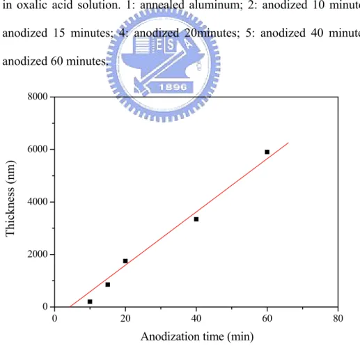
Fig. 4-4 The correlation between the thickness of porous alumina membranes and anodization time.
40
Fig. 4-5 X-ray diffraction profile of porous alumina membranes produced in sulfuric acid solution, oxalic acid solution, and phosphoric acid solution.
40
Fig. 4-6 PL spectra of the aluminum sheet and porous alumina
membranes prepared in oxalic acid solution. 1: annealed aluminum; 2: anodized 10 minutes; 3: anodized 15 minutes; 4: anodized 20minutes; 5: anodized 40 minutes; 6: anodized 60
minutes.
Fig. 4-7 Thickness as a function of anodization time when the aluminum sheet was anodized in 0.3 M oxalic acid solution.
42
Fig. 4-8 PLE spectra monitored at 440 nm (a) and 470 nm (b) for the aluminum sheet and porous alumina membranes prepared in oxalic acid solution. 1: annealed aluminum; 2: anodized 10 minutes; 3: anodized 15 minutes; 4: anodized 20minutes; 5: anodized 40 minutes; 6: anodized 60 minutes.
45
Fig. 4-9 Schematic diagram for PL curve of the porous alumina membranes whose spectra have been deconvoluted by Gaussian functions (A and B curves) and the dense alumina (C curve).
46
Fig. 4-10 PL spectra of the aluminum sheet and porous alumina
membranes prepared in different acid solution, 1: annealed aluminum; 2: 10 wt% sulfuric acid; 3: 0.3 M oxalic acid; 4: 0.1 M phosphoric acid. The insert is an enlargement of the curve 4.
47
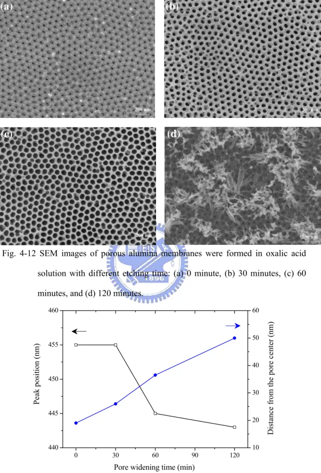
Fig. 4-11 PL spectra of porous alumina membranes prepared in oxalic acid solution, 1: as prepared sample; 2: pore widening 30 minutes; 3: pore widening 60 minutes; 4: pore widening 120 minutes.
48
Fig. 4-12 SEM images of porous alumina membranes were formed in oxalic acid solution with different etching time: (a) 0 minute, (b) 30 minutes, (c) 60 minutes, and (d) 120 minutes.
50
Fig. 4-13 The variations in the PL peak position and the distance from the center of the nanopore at the different pore widening time.
50
Fig. 5-1 SEM images of Pb nanowires with diameters of 20 nm (a), 80 nm (b), 200 nm (c) and 300 nm (d).
Fig. 5-2 TEM morphologies of the Pb nanowires with diameters of 20 nm (a) and 80 nm (b). The inserts in (a) and (b) are the selective area electron diffraction pattern of the corresponding Pb wire. (c) and (d) are the TEM images of the Pb nanowires with diameters of 200nm and 300nm, respectively. The grain boundaries are indicated by arrows.
55
Fig. 5-3 The cross-section images of the porous alumina membrane with pore size about 200 nm (a) and 80 nm (b).
56
Fig. 5-4 The X-ray diffraction spectra of Pb nanowires with 20, 80, 200 and 300 nm average diameter.
56
Fig. 5-5 Relationship between the change in Gibbs free energy and the reaction temperature.
59
Fig. 5-6 Relationship between the partial pressure of the oxygen and the temperature in the reaction: 3Pb(s,l) +2O2(g) →Pb3O4(s).
60
Fig. 5-7 The curve of required force with pore diameter when Pb melt is injected into the nanochannel.
60
Fig. 5-8 Schematic illustration of the the Pb nanowire solidification model. Here, Z is the coordinate with respect to the moving solid-liquid interface and V is the rate of the movement of the solid-liquid interface.
63
Fig. 5-9 The Gibbs free energies of various reactions forming PbS. 68
Fig. 5-10 Relationship between the change in Gibbs free energy and the reaction temperature.
69
Fig. 5-11 (a) SEM image of a porous alumina membrane produced in 0.3 M oxalic acid solution. (b) SEM image of Pb nanowires
fabricated by vacuum pressure injection process. The morphologies of the PbS nanocrystals prepared via the reaction between Pb wires and S vapor at various time: (c) 3 hours and (d) 8 hours.
Fig. 5-12 X-ray diffraction profiles of Pb nanowires (80 nm) and PbS nanocrystals with different sulfization time (S vapor).
70
Fig. 5-13 SEM images of the PbS nanoparticles fabricated by sulfization process with H2S gas: (a) 473 K 8 hours; (b) 573 K 8hours; (c) 673 K 8 hours; (d) 573 K 6 hours and (e) 573 K 3 hours.
72
Fig. 5-14 X-ray diffraction profiles of Pb nanowires (80 nm) and PbS nanocrystals with different sulfization time (H2S gas) at 573 K.
73
Fig. 5-15 (a) SEM image of a porous alumina membrane produced in 10% sulfuric acid solution. (b) SEM image of Pb nanowire arrays fabricated by vacuum pressure injection process. The morphologies of the PbS nanocrystals prepared at various time: (c) 1hour; (d) 3 hours; (e) 6 hours and (f) 8 hours.
75
Fig. 5-16 The size distribution of the PbS cubes with different sulfization time: (a) 1 hours; (b) 3 hours; (c) 6 hours and (d) 8 hours.
76
Fig. 5-17 Relationship between average edge length of PbS nanocubes and sulfization time.
77
Fig. 5-18 Representative XPS spectra of the Al, O, S and Pb in the as-prepared PbS sample.
78
Fig. 5-19 X-ray diffraction profiles of Pb nanowires and PbS nanocrystals with different sulfization time.
79
electron diffraction pattern of the Pb wire. (c) Low magnification TEM image of the PbS sample with 1 hour sulfization exposed to H2S gas at 573 K. (d) Energy- dispersive X-ray spectrum recorded from a PbS nanocube (the circular area in (c)). (e) High resolution TEM image of a single PbS nanocrystal. (f) TEM morphology of the PbS nanocube as the reaction time was 3 hours.
Fig. 5-21 (a) Low-magnification TEM image and the corresponding selective-area electron diffraction pattern of a PbS nanoparticle (the circular area) as the reaction time is 6 hours, and (b) Energy- dispersive X-ray spectrum recorded from a PbS nanoparticle (the circular area in (a)).
83
Fig. 5-22 (a) Enlarged TEM image recorded from the marked area in Fig. 5-21 (a); High-resolution TEM images of PbS nanocrystals, (b), (c) and (d), recorded from the areas indicated by A, B and C boxes in (a), respectively.
84
Fig. 5-23 (a) TEM image of the PbS sample with 8 hours sulfization. (b) High resolution TEM image of a single nanocrystal. (c) FFT analysis of the lattice fringes in (b) with the rock salt PbS planes indicated. (d) Inverse FFT lattice fringes image with the (220) spots by Digital Micrograph Software. The dislocations are indicated by arrows.
85
Fig. 5-24 DSC thermographs of Pb bulk, Pb nanowires and PbS
nanocrystals.
87
model.
Fig. 5-26 (a) A series of PL spectra for PbS nanocrystals of different exposure time to H2S gas. (b) Schematic diagram for PL curve of the PbS nanocrystals with 1 hour sulfization time whose spectra have been deconvoluted by Gaussian functions.
Chapter 1 General Introduction
In recent years, there has been a dramatic proliferation of researches concerned with low dimensional materials. The physical properties of one dimensional and quasi-one-dimensional structure have attracted much attraction for fundamental studies and for practical application in electronics and optoelectronics. Nanomaterials in the templates exhibit both optical and transport anisotropy. The effects of the confinement to nanomaterials by the templates are the dielectric enhancement and the optical anisotropic properties. An appropriate infill, such as
Ⅱ-Ⅵ or Ⅳ- semiconductors, Ⅵ can produce the significant broadness of the
electronic transitions resulting from the quantum confinement effect. Quantum confinement effect in low-dimensional systems not only provides a forceful tool for managing their optical, electrical, and thermoelectric properties, but also creates possibilities for nano-technological applications. Because of the distinguished optical and electronic properties, the control of the size and morphologies of nano-materials has been a primary focus.
The electrochemically produced porous alumina membranes with highly ordered nanopore arrays have been widely used as templates for the fabrication of ordered nanostructures with nanocrystals, nanowires or nanorods of various materials. The porous alumina membrane itself owns a strong blue photoluminescence band; nevertheless, the phenomenon is still not very clear. Therefore, detailed optical characteristics are technological importance from the viewpoints of the porous alumina membranes. The synthesized nanomaterials in porous alumina membranes for optical device applications also attract many interests until now.
In this study, lead sulfide (PbS) is chosen as the nanomaterial produced in porous alumina membrane for several reasons.
First, PbS is a narrow band gap semiconductor material that can be readily prepared as nanostructure exhibiting strong quantum confinement effect of charge carriers, electron and hole. PbS nanocrystals in the quantum regime (crystal size smaller than the Bohr radius) have tunable broad band absorption from visible light to near-infrared light. Secondly, electrons and holes are equally mobile, unlike cadmium selenide (CdSe) where electron transport dominates. Thirdly, PbS nanocrystals exhibit a relatively long excited state life time. The distinguishing features make PbS nanocrystals be potentially useful on solar cells, optical switches, light emitting diodes, and optically active component for optoelectronic applications.
The present works are to investigate the photoluminescence properties of porous alumina membranes and to use porous alumina membrane as a template to fabricate the optical nanomaterials, PbS nanocrystals. In chapter 2, we provide a background about the basic concepts, luminescence origins, and classification of luminescence materials. After that, some representative researches about photoluminescence phenomenon of porous alumina membranes are indicated. The most popular methods to fabricate PbS nanocrystals and the emission properties of PbS nanocrystals are also reported in chapter 2. Chapter 3 describes the details of fabrication process of porous alumina membranes and PbS nanocrystals. Subsequently all kinds of characteristic analyses methods are also provided. Chapter 4 reports the morphologies and experimental conditions of porous alumina membranes. We explore the effects of thickness, electrolyte, and pore widening on the photoluminescence intensity of porous alumina membranes as well as explain the emission centers about the luminescence. In chapter 5, thermodynamic calculation and experiment identification of Pb nanowires are first described. Then, we demonstrate the morphologies and structure characteristic of PbS nanocrystals
studied by TEM and thermodynamic calculation. At last, the photoluminescence properties and mechanism of PbS nanocrystals are also provided and explained. In chapter 6, we make a brief conclusion of this work. Finally, a broad concept for future work in this field is given.
Chapter 2 Literature Review
2.1 Photoluminescence of Solids
Luminescence in solids is the phenomenon in which electronic states of solids are excited by some energy from an external source and the excitation energy is released as light. When the energy comes from short wavelength light, usually ultraviolet light, the phenomenon is called photoluminescence.
Photoluminescence can be divided into two major types, namely intrinsic luminescence and extrinsic luminescence. In the former there are three kinds, band-to-band luminescence, exciton luminescence and cross-luminescence. The latter consists of two parts, unlocalized and localized. In unlocalized luminescence, excited electrons and holes of the host lattice participate in luminescence processes. When the luminescence excitation and emission processes are confined to localized centers, this kind of luminescence is called localized luminescence [1].
2.1.1 Intrinsic luminescence
There are three kinds of intrinsic luminescence: band-to-band luminescence, exciton luminescence, and cross luminescence. Here each kind of luminescence will be explained and discussed briefly.
(1) Band-to-band luminescence: Luminescence owing to the band-to-band transition can be observed in very pure crystals at relatively high temperature. For example, an electron in the conduction band recombines with a hole in the valence band. This has been observed in Si, Ge, and some Ⅲ-Ⅴ compounds such as GaAs. At low temperature, this luminescence is transformed into exciton luminescence. From the viewpoint of luminescence application, light emission from light
(2) Exciton luminescence: An exciton is a composite particle of an excited electron and a hole. It moves in a crystal to convey energy and produces luminescence due to the recombination of the electron and the hole. There are two kinds of excitons: the Winnier exciton and the Frenkel exciton. The Winnier exciton model expresses an exciton as composed of an electron in the conduction band and a hole in the valence band bound together by their attractive coulomb interaction. This model works well for inorganic semiconductors such as Ⅲ-Ⅴ and Ⅱ-Ⅳ compounds. The Wannier exciton moves in a crystal but does not contribute to electric conduction because it is electrically neutral. It emits luminescence by the recombination of the electron and hole composing it. This type of exciton is weakly bound, with an average electron-hole distance large in comparison with a lattice constant. Wannier excitons are stable only at relatively low temperatures, where the binding energies of excitons are higher than the thermal energy. At higher temperatures, where the thermal energy is higher, the
excitons are no longer stable and the band-to-band luminescence appears instead. The Frenkel exciton model is used in cases where the distance between the
electron and hole is smaller than the lattice constant. A Frenkel exciton is a tightly bound exciton and essentially an excited state of a single atom. The excitation is localized on or near a single atom because the hole is usually on the same atom as the electron. Typical examples are organic molecular crystals and inorganic complex salts including transition-metal ions. In these materials, the binding within a molecule is strong in comparison with the van der Waals binding between molecules, so that the cxcitons are Frenkel excitons.
(3) Cross-luminescence: Cross-luminescence is produced by the recombination of an electron in the valence band with a hole created in the outermost core band. The luminescence can take place only when the energy difference between the top of
the valence band and that of the outermost core band is smaller than the band gap energy. An Auger process occurs when the hole in the outermost core band is filled nonradiatively with an electron in the valence band and another electron in the conduction band is dropped to the valence band with energy release as luminescence. Therefore, cross-luminescence is observable only in materials satisfying the condition.
2.1.2 Extrinsic luminescence
Luminescence caused by intentionally incorporated impurities, such as metallic impurities or defects, is classified as extrinsic luminescence. Most of the observed types of luminescence that have practical applications belong to this category. Intentionally incorporated impurities are called activators and materials made luminescent in this way are usually called phosphors. Extrinsic luminescence can be divided into two types: unlocalized and localized. In the unlocalized type, the electrons and holes of the host lattice can participate in the luminescence process. In the case of the localized type, the luminescence excitation and emission processes are confined in a localized luminescence center.
(1) Unlocalized luminescence: In semiconductors, most important impurities are donors and acceptors that dominate semiconductive properties, and these act as luminescence activators. Donor-acceptor pair luminescence is a very important example of the unlocalized extrinsic type. Electrons excited into the conduction band are captured by ionized donors, and the holes in the valence band are captured by ionized acceptors. The emission involves electron transfer between neutral donors and neutral acceptors. Therefore, the emission energy of this luminescence generated on a donor-acceptor pair depends on the distance
Another important luminescence of the unlocalized type is isoelectronic traps. If an impurity atom is introduced and replaces or substitutes for the host atom in a semiconductor, it attracts an electron or a hole because of the difference in electron affinity. Such a substitutional atom is called an isoelectronic trap. When the electron affinity of the introduced atom is larger than that of the host atom, the substitutional atom can become an electron trap. If an electron is trapped, a hole is attracted through the coulomb interactive force. In this way, a bound exciton is formed and luminescence is produced. In addition to these mentioned above, the unlocalized luminescence is very important in terms of practical applications.
(2) Localized luminescence: Various kinds of metallic impurities intentionally incorporated in the ionic crystals and semiconductors often create efficient localized luminescence centers. In the localized luminescence, the impurity atoms form the emission centers in the semiconductor. These centers are essentially closed and do not couple with the host atoms. Therefore, the luminescence properties are primary decided by the emission centers and the host material almost has no influence on the luminescence. Localized type centers with regard to energy transitions are classified into: allowed-transition type, and forbidden-transition type. Energy levels of localized centers are seen in the energy band scheme in Fig. 2-1. In the case of A, both the ground and the excited states are located in the forbidden gap. In the case B, the states are embedded in or located below the valence band. There are many intermediate cases between A and B. Localized centers can be also excited by the band-to-band transition as shown by C and D in Fig. 2-1. In the case of C, first a hole is captured by the center and then an electron is captured to produce luminescence. In the case of D, the electron is captured first and then the hole.
Fig. 2-1 Energy levels of localized centers and luminescence transition [1].
2.1.3 Classification of luminescent materials
Luminescence is the emission of optical radiation resulting from nonthermal excitation of the energy levels of atoms, molecules, polymers, and crystals.
Luminescent materials can be classified into several broad groups [2, 3]:
(1) Aromatic molecules: These kinds of materials luminesce in the vapor phase, liquid phase, solid phase, and in fluid or rigid solutions. They constitute the large group, and are used widely in luminescent dyes and paints, fabric and paper brighteners, dye laser, etc.
(2) Inorganic crystals: These types of materials include diamond, ruby, alkali halides, zinc sulfide, calcium tungstate and so on. Their emissions are usually efficient, and result from impurity centers or crystal defects. Luminescent inorganic crystals are used for scintillators, luminescent screens, solid state lasers, jewelry, etc.
(3) Noble gases (He, Ne, Ar, Kr, Xe): These materials luminesce in the vapor phase, liquid phase, solid phase, and solutions. They are used in discharge lamps, gas lasers, and scintillators.
(4) Simple inorganic molecules: These molecules usually luminesce in the vapor phases. Some like H2, D2, N2, and Hg, are used in discharge lamps as well as others (N2, I2, and CO2) are applied to gas lasers.
(5) Inorganic ions: These ions notably of the rare earths are used as activators in crystals, glasses, and chelates. Applications include inorganic and glass scintillators, and glass lasers.
(6) Aliphatic molecules (paraffins and cyclohexane): These kinds of molecules are now known to emit in the far UV with a low photon yield.
Whole not exhaustive, this list illustrates the wide range of luminescent materials and their applications.
2.2 Optical properties of porous alumina membranes
Optical properties of aluminum oxide have been investigated since 1970s. Ultraviolet absorption, emission and excitation spectra were studied for high-purity crystalline alumina by Evans [4]. Crystallized alumina [5], including α-, γ-, and η phases, or sapphire [6-7] doped with titanium and chromium ions had also reported the optical behaviors by using various methods from the 70’s to the 90’s. The photoluminescence properties of the electrochemically produced porous alumina membranes were increasingly investigated in the late 20th century because of the potential use in optoelectronics and nanotechnology. Although many studies have been done on the optical properties of crystalline alumina, little information is available on the optical behaviors of porous alumina membranes. Due to the mechanisms and the characterization of the photoluminescence band are quite complex, the photoluminescence phenomenon has been studied by several researches until now. There are three major models to explain this phenomenon stated in following paragraphs.
Du and his co-works [8] reported that a very strong PL band of the porous alumina membrane anodized in oxalic acid solution was observed when excited by a Xe lamp. Figure 2-2 shows a broad PL band centered about 450 nm occurs in the wavelength of 400-600 nm. The process parameters of the tested samples are shown in table 2-1. The intensity of the PL band increases with the heat treatment temperature, Ta, and reaches a maximum when Ta is 773 K. Electron paramagnetic resonance (EPR) measurement are carried out to find the origin of the blue PL band, as shown in Fig. 2-3. It describes that an obvious EPR signal appears in the spectrum. This means that there are many singly ionized oxygen vacancies (F+ centers) in the porous alumina membranes because other oxygen vacancies (F and F++ centers) are not paramagnetic. Oxygen vacancies have several categories, such as F, F+, F++, etc. F means an oxygen vacancy with two electrons, F+ center is formed by an oxygen vacancy trapping an electron, and F++ is an oxygen vacancy without electron. Therefore, the authors thought that the PL band originated from single ionized oxygen vacancies (F+ centers) in the porous alumina membranes. The similar results were also described in other reports [9-10]. Li et al. [9] observed that the PL band peaking around 470 nm in the wavelength range of 200 nm to 500nm was caused by the F+ centers of the porous alumina membrane with excitation wavelength of 360 nm. The PL properties from silicon based porous alumina films were also investigated by Wu et al. [10]. The PL spectra of as anodized samples showed that there were three strong PL bands centered at 295, 340, and 395 nm with an excitation wavelength of 240 nm. They suggested that oxygen-related defects, F+ centers, were responsible for the observed PL peaks.
Fig. 2-2 PL spectra of porous alumina membranes and the porous silicon [8]. Table 2-1 Parameters of the heat treatment for the porous alumina membranes [8].
sample conditions a as prepared b 473 K for 4 hours c 573 K for 4 hours d 673 K for 4 hours e 773 K for 4 hours f 823 K for 4 hours
g aging in air for 15 days after heating at 823 K for 4 hours
h annealing at 823 K in H2 for 1 hour after aging in air for 15 days
Fig. 2-3 EPR trace at room temperature for porous alumina prepared in oxalic acid [8].
A further investigation of PL properties from alumina membranes anodized in 0.5 M oxalic acid solution was reported by Huang and his co-works [11]. Figure 2-4 shows that a PL peak in the Blue can be divided into two bands around 405 nm and 455 nm. From the spectra, the intensity of the 455 nm band relative to the 405 nm band increases with the electrolyte concentration. When the electrolyte concentration increases, the current is larger and more charge carriers can move to the alumina. Moreover, the oxygen vacancies in porous alumina membrane can trap two electrons easily, and the density of the F center becomes larger. Therefore, the writers suggested that the two luminescent bands arose from two kinds of different defects (F and F+ centers) rather than only one kind of defect center, F+, as reported previously. A defect distribution model in the alumina membrane also presents as shown in Fig. 2-5. The density of the F centers is the largest near the surface because the oxygen vacancies located on the surface can easily trap two electrons and become the F center. Then, the density of the F centers decreases gradually with an increase in the pore wall depth. The situation of the F+ centers is just reversed.
Fig. 2-4 The PL spectra of the alumina membranes obtained by anodization of Al foils in 0.5, 0.23, and 0.1 M oxalic acid solutions [11].
Fig. 2-5 A model for distribution of the F (dark square) and F+ (open square) centers in the alumina membranes [11].
The Second model concerning the origins of the blue PL band in porous alumina membranes was proposed first by Yamamoto et al. [12]. They reported that the oxalic impurity was the reason for the blue PL band. Later research by Gao et al. [13] supported the viewpoint of Yamamoto et al. Figure 2-6 shows the PL excitation
and emission spectra of the alumina films anodized in 0.3 M oxalic acid solution in the ultraviolet-to-green region. In Fig. 2-6 (b), an intensive and broad PL emission band peaks around 470 nm. The corresponding excitation spectrum shown in Fig. 2-6 (a) describes that a major excitation band around 360 nm and a weaker side band located around 250 nm are observed. From the results of PL and PLE spectra, it can be suggested that the 470 nm emission band is related to the two excitation centers. Figure 2-7 shows that the intensity of the 470 nm PL emission peak and the intensity of the EPR signal peak for the alumina films vary as a function of annealing temperature. The intensity of the 470 nm PL emission increases with the rise of the temperature, meanwhile, the intensity of the EPR signal decreases with the rise of the temperature. This reveals that the origin of the 470 nm emission band is different from that of the EPR signal. In addition, during the anodization process, the oxalic impurities can be incorporated into porous alumina films [12]. The dissociation of acids generates conjugate base anions (from reaction 1 and 2), and the conjugate base anions can partly replace the O2- in the alumina film.
+ − + →HC O H O C H2 2 4 2 4 (2-1) HC2O4− →C2O42− +H+ (2-2)
It is reasonable that the incorporated impurities existing in the alumina films have important influences on their optical properties. Therefore, Gao et al. concluded that the evidence for F+ centers in oxalic alumina membranes was slight. The PL centers produced from the incorporated oxalic impurities during the anodization process were responsible for the 470 nm blue luminescence.
However, the details of the oxalic impurities existing in the alumina films anodized in oxalic acid solution, such as their exciting and distributing forms, are not very clear at present.
Fig. 2-6 The PL excitation (a) and emission (b) spectra of the porous alumina film anodized in oxalic acid solution [13].
Fig. 2-7 The intensity of the 470 nm PL emission peak and the EPR signal of the oxalic alumina film as a function of annealing temperature [13].
The last model describes F+ centers and the oxalic impurities are both the origins of the PL band in porous alumina membranes. Li et al. [14] indicated that a PL band range from 300 to 600 nm was observed. The PL intensity and peak position depended strongly on the excitation wavelength. Figure 2-8 shows that there are two peaks in the PL band: one (P1) is at constant wavelength of 460 nm, and the other (P2) increases almost linearly from 420 to 465 nm with excitation wavelength. The authors concluded that there were two PL centers, one originating from the
oxygen-related defects in the barrier layer (the relatively pure alumina), contributing mainly to the second PL band (460 nm), and the other correlated with the aluminum incorporated into the anion-contaminated alumina layer, contributing mainly to the first PL band (420 ~ 465 nm). The similar phenomenon was also observed by Li and his co-works [15]. Indeed, they suggested that there were three optical centers in the annealed alumina membranes. Due to the F+ centers could convert to F centers at high temperature annealing, the first was originated from the F center, the second was correlated with F+ centers, and the third was associated with the oxalic impurities incorporated in the alumina membranes.
Fig. 2-8 (a) PL emission spectra for porous alumina membranes prepared in oxalic acid solution.(b) The Gaussian fitting of emission spectra with the changes of Gaussian fitting peak position and PL intensity with wavelength [14].
2.3 Reviews of the PbS nanocrystals
2.3.1 Fabrication processes of PbS nanocrystals
Various approaches producing PbS nanocrystals have been developed for years. The different methods for PbS nanocrystals fabrication can be divided into two main categories: PbS nanocrystals not embedded in a matrix and embedded in an attached materials.
(1) PbS nanocrystals not embedded in a matrix
One of the most used chemical routes to produce PbS nanocrystals is colloidal chemistry [16-19]. This method consists in the reaction of the lead precursor (typically a lead salt: lead acetate, nitrate, or perchlorate) and sulfur precursor (usually H2S, Na2S or CS2) in suitable solvents. In this method, the nucleation and growth processes are controlled through suitable stabilizer (capping agent), temperature, solvents, and pH values. Among these factors, the capping agent plays a very important role in controlling the surface states and the optical properties of the PbS nanocrystals.
PbS nanocrystals have also been synthesized using a micelles mediated colloids methods [20-22]. Zhang and his co-works [20] prepared a microemulsion in the system, surfactant/isooctane/water, allowing the reaction between the lead and sulfur precursors inside the micelles. In the system, the surfactant tended to self-associated to minimize contact with water molecules, resulting in the formation of various aggregates with the concentration change of the surfactant. Figure 2-9 shows a possible micelle with a rod-like shape. The water pool within the micelle can be divided into two parts, one part is in the region similar to the shell of a peanut, and the other part is in the sphere micelles just like the peanuts. Thus it can be seen that the size and shape of the products usually depend on the size and shape of the micelles.
Fig. 2-9 Schematic illustration of a possible micells: (a) the cross section of the short axis, (b) the cross section along the long axis [20].
Fig. 2-10 (a) TEM image of PbS nanocubes [26]; (b) SEM image of star-shaped PbS nanocrystals [25]; (c) SEM image of star-shaped PbS dendrites with six arms [26]; (d) SEM image of PbS hollowed cube [25].
PbS nanocrystals were also obtained through a thermal decomposition process [23-26]. Most of the above researches produced near spherical PbS nanocrystals, however, a variety of morphologies of PbS nanocrystals such as cubes, rod-like shapes, wires, truncated octahedrons, dendrites, star-shapes, and flower-shaped structures, had been achieved by thermal decomposition method.
A
Figure 2-10 shows some PbS nanocrystals with different morphologies prepared by thermal decomposition method. The morphologies of PbS nanocrystals can be controlled by choosing suitable reaction temperature, adjusting pH value, and concentration of precursors.
Other methods, such as chemical deposition [27-28], chemical vapor deposition [29], electrochemistry [30], microemulsion [31], and microwave assisted synthesis [32-33] have been also used to prepare PbS nanocrystals.
(2) PbS nanocrystals in a attached materials
PbS nanocrystals have been embedded in many different kinds of host materials as films or bulks. Polymers are one of the most used matrices to embed PbS nanocrystals [34-40]. A polymer matrix is usually chosen because of uniform and optical transparent properties. Wang et al. [34] used poly(vinyl butyral) (PVB) as a matrix, which acted as both a stabilizer and a robust template, for the nanocrystals growth. Rod shaped PbS nanocrystals were formed inside the PVB film using Pb(AOT)2, (bis(2-ethylhexyl)sulfosuccinate), as the precursor upon
exposure to H2S. PbS nanocrystals in the conducting polymer MEH-PPV,
poly(2-methoxy-5(2’-ethyl-hexyloxy)-p-phenylene vinylene), were also obtained for the optoelectronic application [35-36]. The conjugated polymer MEH-PPV was used to control the nanocrystal growth and passivate surface states. The conjugated polymer could act as a colloidal template, and therefore, the nanocrystals self assembled are highly crystalline. A typical example is shown in Fig. 2-11. As prepared PbS nanocrystal in MEH-PPV has a single crystal structure.
Fig.2-11 (a) TEM image of a dilute sample of PbS nanocrystals; (b) HRTEM image of the lattice planes in a single nanocrystal (bar =1 nm) [35].
PbS nanocrysatls were also produced on the internal surface of a nanoporous TiO2 template. During the process, the TiO2 template was put into a concentrated sol-gel solution to coat lead ions and followed by immersing in Na2S solution to produce PbS nanocrystals on the TiO2 template [41-43]. In this process, the PbS nanocrystals about 3 nm in diameter were obtained, while larger crystals about 3~10 nm also existed when the immersing process was repeated several times.
Glasses doped with PbS nanocrystals had also been prepared by a traditional glass melting technique [44-45]. Lipovskii et al. [44] melted the materials including sulfur at a temperature about 1373 K, and then promoted the nucleation and growth of the nanocrystals while annealing the sample just over the glass transition temperature in reducing atmosphere. In this process, the size and size distribution of PbS nanocrystals was strictly related to the heat treatment schedule.
2.3.2 Emitting properties of PbS nanocrystals
The effects of dimensional confinement on the optical properties of the materials whose bulk phases exhibit a relatively free motion of electrons have been studied for many years. Basically, the effects can make the materials to produce a blue shift in the band gap and appear some discrete sub-bands in the energy band. As
the dimensions of confinement increase, the band gap decreases, and therefore the band to band transitions shift to longer wavelengths, finally approaching the bulk value for a large width. Quantum confinement of electrons and holes also leads to enhanced binding between them and thereby produces increased exciton binding energy compared to the exciton binding energy for the bulk materials, list in table 2-2.
Table 2-2 Semiconductor materials parameters [46-49].
Materials Band gap
energy (eV) Band gap wavelength (µm) Exciton Bohr radius (nm) Exciton binding energy (meV) CdS 2.58 0.48 2.8 29 CdSe 1.89 0.67 4.9 15 GaN 3.42 0.36 2.8 GaP 2.26 0.55 10~6.5 3.5 GaAs 1.42 0.87 12.5 5 Si 1.11 1.15 4.3 15 PbS 0.41 3.02 18 4.7
The exciton Bohr radius gives an estimate of the size of the exciton (the most probable distance between the electron and the hole) in a semiconductor. Exciton Bohr radius or often simply the Bohr radius of a specific semiconductor, aB, is defined as: 2 2 e aB µ εh = (2-3)
In the above equation, ε is the dielectric constant of the material, h is Planck constant, and µ is the effective mass of the electron- hole pair defined as:
h e h e m m m m + = µ (2-4)
Here, me is the effective mass of electron, and mh is the effective mass of hole. Besides the Bohr radius, the nature of the confinement is associated with other two lengths: ae and ah. The electron radius ae and the hole radius ah are indicated as:
22 e m a e e h ε = (2-5) 22 e m a h h h ε = (2-6)
In PbS, the Bohr radius aB is 18 nm, and the electron and hole radii are both about 10 nm [50]. The confinement of both electron and hole can be more easily achieved than other semiconductor, like CdSe (ae~3 nm, ah~1 nm). Therefore, a strong quantum confinement effect can be observed in PbS nanocrystals, with the radius of nanocrystal R ﹤aB, and R ﹤ae, ah [51].
Quantum confinement in the PbS nanocrystals results in an increase of the band gap. The larger band gap can cause a strong blue shift of absorption band and emission band to visible or near-infrared wavelengths. Many research groups have revealed the blue shift phenomenon of optical spectra in PbS nanocrystals, as listed in table 2-3. It can be seen that the photoluminescence spectra of PbS nanocrystals change markedly with the morphologies and the procedures used. The emission band can occur in a wide range from 300 nm to 1600 nm. Most of the published results contain only one emission peak which can be attributed to the PbS nanocrystals. Warner et al. [52] described that PbS nanocrystals with 1 nm in diameter are synthesized by colloidal techniques and capped with oleic acid. Fig. 2-12 shows the PbS nanocrystals with 1 nm in diameter have an absorption band edge at 580 nm and exhibit an emission peak centered at 770 nm. It also suggests that lower synthesis temperature yield the smaller PbS nanocrystals. This is typical of the PL spectra that the peak position displays a red shift as the crystal size increases.
Table 2-3 Optical experimental results of PbS nanocrystals.
State diameter Absorption PLE PL Ref.
Oleic acid capped PbS nanocrystals
1~2 nm 580~900 nm 700~900 nm 52
PbS quantum dots in oxide glass 8.5 nm 0.65, 0.85, 1.1 eV 48
Surface passivation PbS nanocrystals 3 nm 636 nm (1.95 eV) 53 PbS nanocrystals 3.3 nm 250 nm 300, 335, 363 nm 54 Surface passivation PbS nanocrystals 2~3 nm 3.44 eV 653 nm (1.9 eV) 55, 61 Alkanethiolate-protected PbS nanocrystals 2~4 nm 560~800 nm 655 nm 804 nm 56 PbS nanocrystals 4 nm 600, 400, 300 nm 700 nm 57
PbS monomers and dimmers in a UV curable sol-gel matrix
510, 810 nm 58
PbS nanocrystals in porous Si 5 nm 665 nm (1.87 eV) 59
PbS nanocrystals in a conjugated polymer 5 nm 1200 nm 1000~1600 nm 60 PbS nanocubes 83 nm×59 nm×22 nm 39 nm×10 nm×7 nm 246~275 nm 434 nm (2.86 eV) 62
State diameter Absorption PLE PL Ref.
PbS nanocystals in silicate glass 3~4 nm 1000~1500 nm 63
PbS nanoparticles in PVA solution
less than 15 nm 540 nm (~2.3 eV) 1100 nm 64
Nano-PbS/ polymer composites less than 10 nm 317 nm 65
PbS nanocrystals in toluene solution
6.5 nm 1300 nm 1350 nm 17
PbS quantum dots in PMMA 850, 950 nm 66
PbS crystals with the clover-like structure
600 nm
(from the apex to the center)
259, 280, 324.5 nm 414 nm 649 nm 33
PbS nanocrystals doped silica film
1~2 nm 311 nm 446 nm 67
PbS hollow spheres 10 nm (size of crystallites)
20 nm (thickness of sphere shell) 500 nm (diameter of sphere)
Fig. 2-12 (a) Absorption spectra of oleic acid capped PbS nanocrystals prepared at 50, 75, 100, 130℃. (b) Fine tuning of the photoluminescence spectra of oleic acid capped PbS nanocrystals as the temperature is varied between 40 and 130 ℃ [52].
a
Chapter 3 Experimental procedures
3.1 Fabrication of porous alumina membranes
General commercial aluminum foils with purity of 99.7 wt % were used to produce porous alumina membranes. The aluminum sheets first annealed at 673 K for 3 hours to release the mechanical stresses of the substrate and then electropolished. After electropolishing, two-step anodization process was progressed. In the first anodization process, the treated aluminum sheet was anodized in an acid solution under a particular condition with a platinum plate as the cathodic electrode. The detailed experimental parameters are list in table 3-1. The pre-formed alumina was removed by wet etching in the mixture of phosphoric acid (6 wt %) and chromic acid (2 wt %) until it entirely dissolved. The sample was anodized again under the same condition like the first anodization. The thicknesses and pore sizes of templates were controlled by choosing suitable anodizing conditions. Hexagonally ordered pores were obtained on the aluminum surface after the entire anodization process. Then, the remaining aluminum was removed in a saturated CuCl2 solution and finally cleaned the sample thoroughly in distilled water.
Table 3-1 3 sets of parameters for anodization of aluminum polished foils in this study.
Electrolyte Concentration Voltage (V) Temperature (K)
H2SO4 10 wt % 18 281
H2C2O4 0.3 M 40 293
3.2 Formation of Pb nanowires in the porous alumina membranes
To investigate the properties of the 1D quantum wire system, a template is usually used to fabricate various material nanowires. Porous anodic alumina membranes with average channel diameters of 20, 80, 200 and 300 nm were used as templates in this experiment.The fabrication of the Pb nanowires was based on the pressure casting process of melted metal. The purity of the initial lead was 99.99 wt %, while the content of impurities did not exceed 10-2 wt %. An alumina template, still attached to Al substrate, and a piece of Pb metal were placed inside the vacuum chamber. Meanwhile, the vacuum pressure was maintained at 10-6 Torr to prevent the active metal oxidation. A hydraulic force was applied on the Pb melt to inject the melt into the nanochannels of the porous alumina membrane. Solidification proceeded using a water cooling method at the bottom of the chamber. We adopted a quenching procedure during Pb melt solidification to separate the nanowire and the remaining metal on the anodic alumina template. Then, the Pb nanowires were formed after cooling to room temperature. This quenching procedure could provide a steep temperature gradient between the nanowires and remaining metal. We could easily obtain the Pb nanowire arrays inside the alumina membrane.
3.3 Production of PbS nanocrystals
The fabrication procedures of the PbS nanocrystals are shown in Fig.3-1. Firstly, the porous alumina membranes as templates were fabricate after the anodization of the published aluminum foils (99.7 wt %) in 10 wt % sulfuric acid solution (H2SO4) and 0.3 M oxalic acid solution (H2C2O4). The nanochannel structures with diameters of 20 nm and 80nm were obtained on the Al substrate. Secondly, a piece of Pb metal and an anodic aluminum oxide template were placed inside an ultra-vacuum chamber. After the chamber was heated to 673 K, a hydraulic force was applied to inject the Pb melt into the nanochannels. When the Pb melt solidified, the Pb nanowire arrays formed in the alumina membrane.Finally, a sulfization procedure was proceeded to obtain PbS nanocrystals. Two different methods were adopted to fabricate the PbS nanocrystals in this study. The first process was that the PbS nanocrystals produced via the reaction between Pb nanowires and sulfur vapor. Pb nanowires with the porous alumina membrane and sulfur powders were sealed in a vacuum glass tube. The tube was put in a furnace with heat treatment at 573K for 3 and 8 hours. The sulfur vapor reacted with the Pb nanowires and the PbS nanocrystals were produced then.
The second method was using H2S gas to produce the PbS nanocrystals. The nanowires were put into a gaseous furnace full of H2S gas whose flow rate was 30 milliliter/minute and applied a heat treatment at 573 K for 1, 3, 6, 8 hours. Finally, the PbS nanocrystals were produced on/in the porous alumina membrane.
Fig. 3-1 Schematic diagrams of PbS nanocrystals fabricated in this work. Al Al Al Al Al Pb bulk Pb bulk Al (a) (b) (c) (d) (e) (f) PbS porous alumina Pb wire
3.4 Characteristic analyses
Characterization of nanomaterials and nanostructures is largely based on the
surface analysis techniques and conventional characterization methods developed for bulk materials. Various structural characterization methods, some typical physical and chemical characterization techniques are discussed following.
3.4.1 Structural characterization X-ray diffraction (XRD)
X-ray diffraction analysis is a kind of non-destructive analytical technique and has very widely applications on material science including phase identification and the crystal structure of solids, identification of unknown materials, orientation of single crystals, preferred orientation of polycrystals, etc. In X-ray diffraction, a collimated beam of X-rays is incident on a specimen and is diffracted by the crystalline phases of the specimen according to Bragg’s law. The diffraction pattern is used to identify the specimen’s crystalline phases and to measure its structural properties. In this study, the crystal structures of porous alumina membranes, Pb nanowires, and PbS nanocrystals were analyzed by X-ray diffraction (Cu Kα, λ= 1.5418 Å, Siemens D5000).
Scanning electron microscopy (SEM)
When the electron probe illuminates the specimen, secondary electrons, backscattered electrons, transmitted electrons, characteristic X-ray, and so forth are emitted from the specimen surface. A scanning electron microscope is a type of electron microscope and a useful tool for high resolution image observation. The surface image of the specimen is obtained from the signals
Morphologies of the porous alumina membranes, Pb nanowires and PbS nanocrystals were observed by a JEOL JSM-6500 scanning electron microscope in this study.
Transmission electron microscopy (TEM)
TEM is a powerful tool to understand the structural features and chemical information at a spatial resolution less than 1 nm of materials. When materials are in the nanometer scale, most of properties and behaviors observed are typically group characteristics corrected from a large number of nanostructural materials. Characterization and measurement of individual nanostructures require not only extreme sensitivity and accuracy, but also ultra-high resolution. A TEM with a finely focused electron probe can provide a complete structural characteristic of a single nanocrystal. In this study, the investigations of the nanowires and nanocrystals were carried out with a Philip Tecnai 20 transmission electron microscope and a JEOL JEM-2100F transmission electron microscope operating at 200 kV.
Atomic force microscopy (AFM)
2D/3D morphologies of the annealed aluminum sheet were determined by the tapping atomic force microscope (Veeco D5000) in this study. AFM is a novel technique for high resolution imaging of conducting as well as non-conducting surface. The physical meaning in AFM is the interaction force between the sample surface and a sharp probing tip. There are three types of imaging modes in AFM: contact, tapping, and non-contact modes. In the tapping mode, the probing tip is periodically in contact with the sample surface and the morphology of the sample is obtained from the change of the
vibration amplitude of the oscillating cantilever.
Focus ion beam (FIB)
In this study, the advanced TEM specimen preparation method of using a focused ion beam miller (FEI Dual Beam FIB) was applied to prepare the cross-sectional TEM specimen. The dual beam FIB system combines an ion beam and a scanning electron beam on the same platform. FIB/SEM technology is also utilized in novel ways to engineer nanostructures and devices using ion and electron beam deposition of metals, organic materials or insulators, as well as milling of materials with the ion beam. The use of FIB for the nanometer precision of TEM specimen preparation has become more and more popular because it is possible to mill very thin membranes from a specific area of a sample.
3.4.2 Physical and chemical characterization Energy dispersive X-ray spectroscopy (EDX)
An energy dispersive spectrometer is usually equipped in an electron microscope. The instrument can also be used as an electron probe microanalyzer for accurate, efficient and non-destructive element analysis or element distribution observation of microscopic areas on the specimen surfaces or cross-sections. This capability is very useful in the fields of materials science such as metals, minerals, semiconductors, and new materials, as well as biological or industrial researches. In the present study, the compositions of nanowires and nanocrystals were detected by energy dispersive X-ray spectroscopy (EDS, Oxford).
X-ray photoelectron spectroscopy (XPS)
X-ray photoelectron spectroscopy, also commonly knows as electron spectroscopy for chemical analysis (ESCA), is used to study the composition and electronic states of the surface region in a sample. It makes use of the photoelectric effect in which an X-ray beam strikes the surface of a material to eject electrons that leave the surface with various energies. This technique is capable of providing information on the oxidation states, immediate chemical environment, and concentration of the constituent atoms. In this study, the chemical compositions of PbS nanocrystals were detected by X-ray photoelectron spectrum (XPS, VG Scientific Microlab 350).
Differential scanning calorimeter (DSC)
Differential scanning calorimeter is a thermal analysis technique which is used to measure the temperatures and heat flows associated with transitions in materials as a function of time and temperature. The operation of a DSC is based on measurement of the thermal response of an unknown substance as compared with an inert reference material when the two specimens are heated or cooled at a constant rate. The difference in thermal response of the two specimens maybe caused by differences in mass, specific heat, heats of reaction or phase transitions, etc. In the present study, the PerkinElmer Diamond differential scanning calorimeter was used to measure the thermal characters of nanocrystals and nanowires.
Photoluminescence spectrometer (PL)
Photoluminescence (PL) is a luminescence caused by ultraviolet, visible, or infrared radiation. PL spectroscopy is a sensitive, non-destructive
technique that can provide valuable information on the type and distribution of defects or impurities in a crystal. Since PL is a characteristic of a given luminescent materials, its measurement can be used for material characterization. In this study, the photoluminescence experiment was performed at room temperature using a Jobin-Yvon Spex Fluolog-3 spectrophotometer with a xenon lamp as the excitation light source. The spectra fitting were executed by the Gaussian functions in the Origin 7.0 software.
Chapter 4 Photoluminescence properties of
porous alumina membranes
4.1 Motivation
In recent years, nanostructure materials have inspired great interest in fundamental study and high-tech industry because they are expected to exhibit very different properties from their bulk forms. Low-dimensional systems represent one of the important fields in advanced material research. Since the development of nano science and technology, researches on porous alumina membranes have drawn much attention. Porous alumina usually contains a hexagonally packed two-dimensional array of cylindrical pores with a relatively uniform size and is often prepared by using anodization of aluminum foils in an anodic medium [69-71]. Due to their regular nanostructure, they have been widely used as templates for fabricating nanostructured materials, such as wires, tubes, and rods for application in the fields of electronics or photoelectronics [72], magnetics [73], energy storage [74], photocatalysis [75], and biosensors [76].
Optical properties of aluminum oxide have been investigated since 1970s. However, photoluminescence property of porous alumina membranes was first studied in 1999. Du and his coworkers reported that a strong and broad PL band was observed in porous alumina membranes anodized in oxalic acid solution [8]. The mechanisms and the characterization of the PL band were complex, and therefore there were many different explanations about this phenomenon. For example, Li et al. suggested that the PL and optical absorption in the wavelength range of 200 nm to 500 nm can be attributed to the F+ centers in alumina membranes [9]. Gao et al. reported that the oxalic impurity was the origin of the PL emission [13].
conducted to understand the PL behavior more clearly. The present study is carried out to determine the relationship between the thickness and the PL properties of porous alumina membranes. In order to establish a reasonable inference to examine the phenomenon, the effect of electrolyte and the distribution of oxalic impurities in porous alumina membrane are also discussed. The results of this study could be useful to understand the mechanism of the optical properties of porous alumina membranes.
4.2 Microstructure observation and characterization of porous
alumina membranes
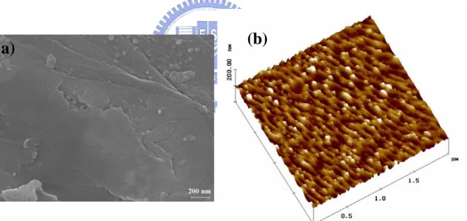
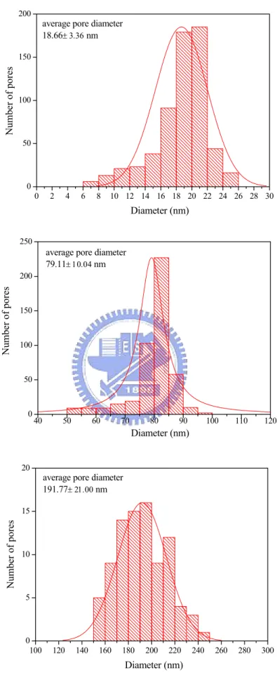
In this study, porous alumina membranes were produced by anodization method by a two-step process in sulfuric acid solution, oxalic acid solution, and phosphoric acid solution. The porous alumina film was found to grow on aluminum with an equilibrium of oxide dissolution at the interface of the alumina / electrolyte and oxide grown at the metal / alumina interface [77]. Figure 4-1 (a) shows that after the aluminum sheet is heat treated at 673 K for 3 hours, there is a thin oxide film on the surface of aluminum. Based on the AFM measurement result (Figure 4-1 (b)), it can be verified that the oxide is a dense alumina with a thickness about 20 nm and the roughness of 5.6 nm. As shown in Figs. 4-2 (a)-(c), the SEM morphologies of porous alumina membranes produced in sulfuric acid solution (a), oxalic acid solution (b), and phosphoric acid solution (c) reveal that the nanopores with different diameters are order and uniform arrays. The corresponding pore size distributions of porous alumina membranes are performed by the histogram analysis. As presented in Fig. 4-3, the histograms are plotted by measuring at least 50 pores in each sample and the average pore diameters are obtained by fitting the histograms with Gaussian
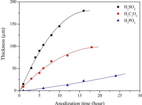
191.77 ± 21.66, respectively. The porosity of each sample is 16.49 %, 36.41%, and 40.72 %. The relationship between anodization time and the thickness of porous alumina membranes anodized in different electrolytes is shown in Fig. 4-4 in which the thickness is measured using SEM microscopy. It can be seen that the alumina membrane anodized in sulfuric acid solution has a faster growth rate than other samples. According to above results, we can understand more clearly about the characters of the porous alumina membranes and prepare the required sample easily by choosing the optimum anodization conditions. Moreover, all the as-prepared alumina membranes are shown to be amorphous in nature as observed by using the XRD technique (Fig. 4-5).
Fig. 4-1 (a) SEM image of an aluminum sheet annealed and (b) AFM image of an aluminum sheet, both annealed at 673 K for 3 hours.
Fig. 4-2 SEM images of porous alumina membranes were formed in (a) sulfuric acid solution, (b) oxalic acid solution, and (c) phosphoric acid solution.
(a)
(b)
0 2 4 6 8 10 12 14 16 18 20 22 24 26 28 30 0 50 100 150 200 Diameter (nm) Numbe r of pore s
average pore diameter
18.66± 3.36 nm 40 50 60 70 80 90 100 110 120 0 50 100 150 200 250
average pore diameter
79.11± 10.04 nm Numbe r of pore s Diameter (nm) 100 120 140 160 180 200 220 240 260 280 300 0 5 10 15 20
average pore diameter
191.77± 21.00 nm
Diameter (nm)
Number of pores
Fig. 4-3 The representative histograms of the porous alumina membranes shown in Figs. 4-2 (a)-(c). The average pore diameters denote in the figures.
0 5 10 15 20 25 30 0 50 100 150 200 Thickness ( µ m)
Anodization time (hour)
H2SO4 H2C2O4 H3PO4
Fig. 4-4 The correlation between the thickness of porous alumina membranes and anodization time. 20 30 40 50 60 H2SO4 H2C2O4 H3PO4 Al2O3 2θ Intensi ty
Fig. 4-5 X-ray diffraction profile of porous alumina membranes produced in sulfuric acid solution, oxalic acid solution, and phosphoric acid solution.
![Fig. 2-2 PL spectra of porous alumina membranes and the porous silicon [8]. Table 2-1 Parameters of the heat treatment for the porous alumina membranes [8]](https://thumb-ap.123doks.com/thumbv2/9libinfo/8399403.179147/29.892.325.625.111.470/spectra-alumina-membranes-silicon-parameters-treatment-alumina-membranes.webp)
![Fig. 2-3 EPR trace at room temperature for porous alumina prepared in oxalic acid [8]](https://thumb-ap.123doks.com/thumbv2/9libinfo/8399403.179147/30.892.317.632.114.388/fig-epr-trace-temperature-porous-alumina-prepared-oxalic.webp)
![Fig. 2-5 A model for distribution of the F (dark square) and F + (open square) centers in the alumina membranes [11]](https://thumb-ap.123doks.com/thumbv2/9libinfo/8399403.179147/31.892.308.625.541.842/fig-model-distribution-square-square-centers-alumina-membranes.webp)