國 立 交 通 大 學
電子工程學系 電子研究所碩士班
碩 士 論 文
超薄絕緣鍺金氧半場效電晶體在量子侷限下的
短通道效應模型與分析
Modeling and Investigation of Short-Channel Effects
for Ultra-Thin-Body Germanium-On-Insulator MOSFETs
Considering Quantum Confinement
研 究 生:謝欣原
指導教授:蘇 彬 教授
超薄絕緣鍺金氧半場效電晶體在量子侷限下的
短通道效應模型與分析
Modeling and Investigation of Short-Channel Effects
for Ultra-Thin-Body Germanium-On-Insulator MOSFETs
Considering Quantum Confinement
研 究 生:謝欣原 Student:Hsin-Yuan Hsieh
指導教授:蘇 彬 Advisor:Pin Su
國 立 交 通 大 學
電子工程學系 電子研究所碩士班
碩 士 論 文
A ThesisSubmitted to Department of Electronics Engineering & Institute of Electronics College of Electrical and Computer Engineering
National Chiao Tung University in Partial Fulfillment of the Requirements
for the Degree of Master in
Electronic Engineering August 2010
超薄絕緣鍺金氧半場效電晶體在量子侷限下的
短通道效應模型與分析
研究生:謝欣原 指導教授:蘇 彬
國立交通大學電子工程學系
電子研究所碩士班
摘 要
鍺作為通道材料已被提出可以提供更高的載子遷移率。然而,它
的高介電常數造成其非常易受到短通道效應的影響。為了改善靜電完
整性,有著薄埋層氧化層的超薄絕緣鍺金氧半場效電晶體被視作一個
有希望的元件結構以繼續 CMOS 的微縮。在本論文裡,我們理論化
地探討在超薄絕緣鍺金氧半場效電晶體中量子侷限效應對臨界電壓
衰變的衝擊。為了獲得臨界電壓,我們解析 Schrödinger 方程式且根
據一個拋物線形式的通道電位來導出量子侷限模型。這拋物線形式的
通道電位是從解 Poisson 方程式得到的通道電位級數解簡化得來,且
此級數解有正確的通道長度依靠性。因此,我們的量子侷限模型可以
用來檢驗超薄絕緣鍺元件的短通道效應。我們的研究指出對於極限微
Modeling and Investigation of Short-Channel Effects
for Ultra-Thin-Body Germanium-On-Insulator MOSFETs
Considering Quantum Confinement
Student:Hsin-Yuan Hsieh Advisor:Pin Su
Department of Electronics Engineering
Institute of Electronics
National Chiao Tung University
Abstract
Germanium as a channel material has been proposed to enable mobility scaling. However, its high permittivity makes it very susceptible to short-channel effects (SCEs). To improve the electrostatic integrity, ultra-thin-body (UTB) germanium-on-insulator (GeOI) MOSFET with thin buried oxide has been proposed as a promising device architecture to continue CMOS scaling. In this thesis, we theoretically investigate the impact of quantum-mechanical effects on the threshold-voltage (V ) roll-off in UTB GeOI MOSFETs. To obtain T V , we have T
analytically solved the Schrödinger equation and derived a quantum-confinement model based on a parabolic form of channel potential. This parabolic channel potential is simplified from the series solution of Poisson’s equation and has the correct dependence of channel length. Therefore, our quantum-confinement model can be used to examine the SCEs for UTB GeOI devices. Our study indicates that for extremely-scaled UTB GeOI devices, V roll-off can be suppressed by quantum T
誌 謝
兩年的碩士生涯即將結束,期間最重要的研究成果,也將會呈現
在這本碩士論文裡。回憶這兩年研究時光所碰到的種種問題與困難,
箇中滋味真是難以言表,所幸最終完成了既定目標,在這論文即將完
成的時刻,心中充滿著感動。
在研究上,最要感謝的是我的指導教授蘇彬老師。老師在其研究
領域的博學多聞以及對於處理問題的方法,都令我印象深刻且受益頗
豐。其中對學生在研究上的耐心建議與指導,更令我感到敬佩。此外,
特別感謝吳育昇學長和 Vita 學姊在這個題目上給我的幫助和建議,
也感謝小郭、銘隆、昆諺三位學長和昌鴻學弟平日裡的討論與關心。
俊賢和劭衡二位學弟雖然相處的時間不長,但能夠在這最後寫論文的
時間和你們聊天對於我壓力的紓解幫助不小,謝謝你們!
最後要謝謝我的家人給我的支持與體諒,兩年的時間很少陪伴在
家人身旁,但父母親的電話關心和與姊姊的 MSN 對話聊天,卻都是我
碩士班兩年的動力來源。有他們的鼓勵,才會有我今日的成就。
Contents
Abstract (Chinese)……..……….….I Abstract (English)...II Acknowledgement...III Contents………..………IV Figure Captions...VI Table Captions...IX Chapter 1 Introduction...1 1.1 Background...1 1.2 Organization...2Chapter 2 Channel Potential Model for Ultra-Thin-Body MOSFETs with Thin BOX Under Subthreshold Region...4
2.1 Introduction...4
2.2 Series Solution of Channel Potential...5
2.3 Compact Form and Verification...9
2.4 Summary...11
Chapter 3 Quantum-Confinement Model for Ultra-Thin-Body MOSFETs with Thin BOX Under Subthreshold Region...19
3.1 Introduction...19
3.2 Model Derivation...19
3.4 Various Channel Materials and Surface Orientations...23
3.5 Summary...26
Chapter 4 Impact of Quantum-Mechanical Effects on Threshold-Voltage Roll-Off in UTB GeOI MOSFETs...37
4.1 Introduction...37
4.2 UTB GeOI Device and Simulation...38
4.3 Results and Discussion...38
4.4 Summary...43
Chapter 5 Conclusions...52
References...53
Figure Captions
Fig. 2.1 Schematic sketch of the UTB structure investigated in this study...13
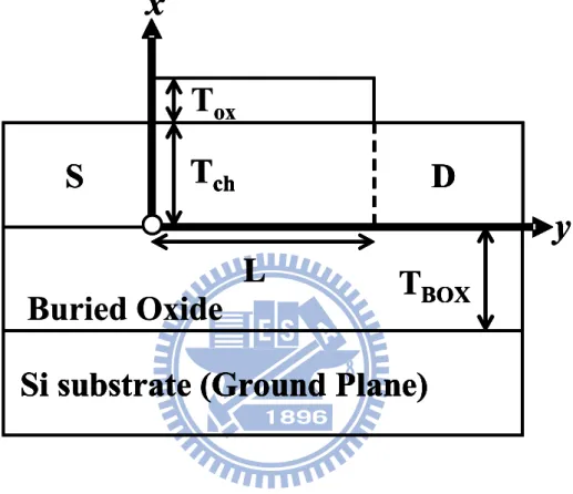
Fig. 2.2 Potential distribution for UTB devices with (a) L=30nm and 15nm and of (b)VDS=0.05V and 1V using model in compact form and series solution...14
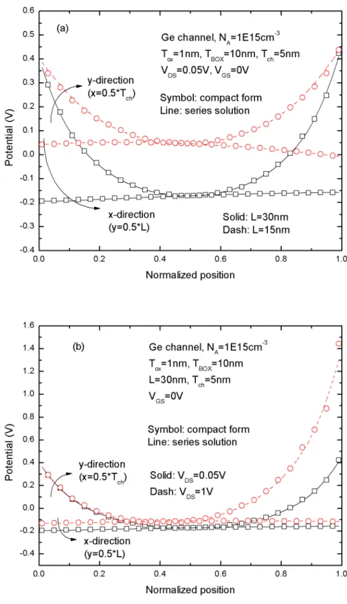
Fig. 2.3 Potential distribution for UTB devices with (a) L=30nm and 15nm, and (b) T =5nm and 10nm using model and TCAD simulation...15 ch
Fig. 2.4 Potential distribution for UTB devices with N =1x10A 15 cm-3, and
N =1x10A 18 cm-3 using model and TCAD simulation...16
Fig. 2.5 Potential distribution for UTB devices with (a) TBOX=5nm, and (b) TBOX=1nm using model and TCAD simulation...17
Fig. 2.6 Potential distribution for UTB devices with (a) VDS=0.05V and 1V, and (b) V =0.2V and 0.5V using model and TCAD simulation...18 BS
Fig. 3.1 The conduction band edge and corresponding eigenenergies for T =10nm ch
devices with (a) L=60nm and (b) L=30nm...27
Fig. 3.2 The calculated quantized n th eigenenergy (E ) for the devices with various n
T ...28 ch
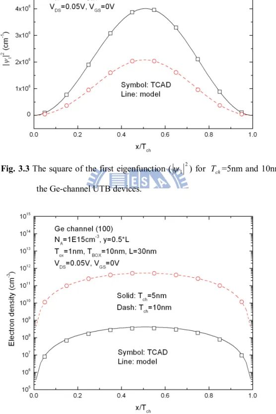
Fig. 3.3 The square of the first eigenfunction (1 2) for T =5nm and 10nm in the ch
Ge-channel UTB devices...29
Fig. 3.4 The electron density for T =5nm and 10nm in the Ge-channel UTB devices. ch
...30
Fig. 3.5 The potential distribution of (a) Si-channel UTB device, and (b)
In0.53Ga0.47As-channel UTB device for model and TCAD results...31
surface orientations with model and TCAD results...32
Fig. 3.7 The
E 1 EC,min
of Ge-channel UTB devices with (a) (110) and (b) (111) surface orientations with model and TCAD results...33Fig. 3.8 The dominant
E 1 EC,min
for UTB devices with various channelmaterials...34
Fig. 3.9 The square of the first eigenfunction (1 2) for (a) Si-channel with (100) surface orientation and (b) In0.53Ga0.47As-channel UTB devices...35
Fig. 3.10 The electron density of Si-channel with (100) surface orientation and
In0.53Ga0.47As-channel UTB devices...36
Fig. 4.1 The V roll-off of Ge- and Si-channel UTB devices with (a) T T =10nm and ch
(b) T =5nm...44 ch
Fig. 4.2
E 1 EC,min
and mQM comparisons between short- and long-channel devices with (a) T =10nm and (b) ch T =5nm...45 chFig. 4.3 (a) The V , (b) the T V roll-off (T VTSCE), and the QM of (100), (110), and (111) surface orientations for T =4nm GeOI devices...46 ch
Fig. 4.4 (a) The V and (b) The T V roll-off of the T Tch=5nm GeOI devices at VDS=0.05V and 1V...47
Fig. 4.5 The GeOI device (Tch=5nm, L=12nm) with VDS=1V shows larger m and
mQM than that with VDS=0.05V...48
Fig. 4.6 (a) The V and (b) The T V roll-off of the T Tch=5nm GeOI devices with TBOX=20nm and 10nm...49
m and mQM than that with TBOX=10nm...50
Fig 4.8 The (VTQMlongchannel VTQMshortchannel) for TBOX=20nm and 10nm GeOI devices at (a) VDS=0.05V and (b) VDS=1V...51
Table Captions
Table 3.1 m*x, d , and md, of three channel materials considering surface
orientations. m is the free electron mass 0 9.111031kg...30
Table 3.2 The critical m*x,crit of three channel materials considering surface orientations when quantum-mechanical effect is strong in ultrathin T ch
Chapter 1
Introduction
1.1 Background
Germanium as a channel material has been proposed [1]-[3] to provide higher mobility for CMOS scaling. However, its higher permittivity makes it very susceptible to short-channel effects (SCEs). To improve the electrostatic integrity, ultra-thin-body (UTB) germanium-on-insulator (GeOI) MOSFET with thin buried oxide (BOX) has been proposed as a promising device architecture and shows better control of SCEs than the bulk counterpart [4]-[5]. As the channel thickness scales down, the quantum-confinement effect may become more significant and its impact on the SCEs of UTB GeOI is not clearly known. In this work, we investigate the problem using theoretical calculations.
Since SCEs are closely related to the subthreshold behaviors of UTB devices and the subthreshold characteristics are deeply influenced by the entire channel potential distribution, an analytical channel potential model is crucial to this study.
An analytical 2-D channel potential model with series form for UTB MOSFETs under subthreshold region has been reported in [6]. Since the series solution of channel potential is too complicated to be used in solving the Schrödinger equation when considering quantum mechanism, we need to simplify the series solution. In this thesis, we present a compact form of the series solution by using a parabolic approximation [7]. Using the parabolic model of channel potential, we can
analytically solve the Schrödinger equation and derive the quantum-confinement model for UTB devices.
Threshold-voltage (V ) roll-off is one of the most important signatures of SCEs, T
and hence V modeling will be a key step to estimate the degree of SCEs. For this T
purpose, the quantum electron density is needed to determine V for various UTB T
devices. So we calculate the quantum electron density by using the derived eigenenergies and eigenfunctions based on our quantum-confinement model.
V. P. Trivede and J. G. Fossum have demonstrated the quantum-mechanical effects on threshold-voltage of undoped double-gate (DG) MOSFET [8]. However, in their study, they only considered the long-channel devices. In other words, the channel potential of cross-section which experiences quantum confinement is always linear [9] and independent of channel length. Nevertheless, for short-channel devices, we have to consider the impact of SCEs on the channel potential distribution.
Since our parabolic channel potential model has included the dependence of channel length, the channel potential along the quantum-confinement direction will vary with the channel length. In other words, our quantum-confinement model based on the parabolic channel potential model can be used to assess the SCEs for UTB devices.
1.2 Organization
potential model of UTB MOSFETs with thin BOX under subthreshold region. In Chapter 3, the quantum-confinement model based on the parabolic channel potential model is derived and we discuss the impact of different channel materials and surface orientations on the degree of quantum confinement. In Chapter 4, we investigate the impact of quantum-mechanical effects on the V roll-off for GeOI devices. Chapter T
Chapter 2
Channel Potential Model for
Ultra-Thin-Body MOSFETs with Thin BOX
Under Subthreshold Region
2.1 Introduction
Ultra-thin-body (UTB) MOSFET with thin buried oxide (BOX) is a promising candidate to extend CMOS scaling because of its superior electrostatic integrity than bulk devices [10]-[12]. In addition, due to its better control of short-channel effects, lower subthreshold swing, and reduced leakage current, UTB MOSFET is also an ideal structure for the subthreshold circuit applications [13]. A channel potential model with series form for UTB MOSFETs under subthreshold region has been reported in [14]-[15]. Using the potential model, the electrostatic characteristics such as threshold-voltage, subthreshold swing, and subthreshold current can be estimated for various UTB devices.
To further simplify the series solution, in this chapter we present a compact form of model to be used in Chapter 3. The model verification is shown in Section 2.3. For various UTB structures with long- and short-channel length, thin- and thick-channel thickness, low and high channel doping concentration, and different buried oxide thickness, comparisons between the model and TCAD simulations have been carried out. Besides, we also examine the model at high and low drain biases and different
2.2 Series Solution of Channel Potential
Our theoretical 2-D potential model for UTB MOSFETs is derived from the Poisson’s equation. Fig. 2.1 shows a schematic sketch of a UTB device with thin buried oxide and silicon substrate. In the subthreshold region, the channel is fully depleted with negligible mobile carriers. Therefore, the channel potential distribution
x y
ch ,
satisfies the Poisson’s equation
ch ch ch ch qN y y x x y x 2 2 2 2 , , (2.1), where Nch and ch are the channel doping concentration and permittivity, respectively. Since there is no charge in the buried oxide region, the buried oxide potential distribution BOX
x,y
satisfies the Laplace equation
0 , , 2 2 2 2 y y x x y x BOX BOX (2.2)The required boundary conditions can be described as [2.5]-[2.6]
G FB T x ch ox ch ox ch ch V V x y x T y T ch , , (2.3a)
ms S ch x V ,0 (2.3b)
ms D ch x L V , (2.3c)
BOX
back gate FBback gate
ich isub
BOX T ,y V V , E, E,
BOX sub i ch i gate back FB gate back S ms sub i ch i gate back FB gate back BOX T E E V V V x E E V V x , , , , , , 0 , (2.3e)
BOX sub i ch i gate back FB gate back D ms sub i ch i gate back FB gate back BOX T E E V V V x E E V V L x , , , , , , , (2.3f)
0 0 , , x BOX BOX x ch ch x y x x y x (2.3g)
0 0 , , x BOX x ch y y x y y x (2.3h), where T , ch T , and ox TBOX are the thicknesses of channel, gate oxide, and buried oxide, respectively. L is the gate length. and ox BOX are the permittivity of gate oxide and buried oxide, respectively. V , G Vbaclgate, V , and S V are the voltage D
biases of gate, back-gate, source, and drain, respectively. V and FB VFB,backgate are the flat-band voltages of gate and back-gate, respectively. is the built-in potential ms
of the source/drain to the channel. Ei,ch and Ei,sub are the intrinsic Fermi level of channel and substrate, respectively.
The corresponding 2-D boundary value problem can be divided into two sub-problems, a 1-D Poisson’s equation and a 2-D Laplace equation. Using the superposition principle, the complete channel potential solution is
x y
ch
x ch
x y
ch , ,1 ,2 ,
, where ch 1,
x and ch,2
x,y
are the solutions of 1-D and 2-D sub-problems in the channel, respectively. The 1-D solution ch 1,
x can be expressed as
x qN x A x B ch ch ch 2 1 , 2 (2.4a)
BOX BOX ch ox ox ch ch ch ox ox ch ch ch ch sub i ch i gate back FB gate back FB G T T T T T T qN E E V V V V A 2 2 2 . . , (2.4b)
back gate FBback gate ich isub
BOX BOX ch T A V V E E B , , . (2.4c)
In solving the 2-D sub-problem, the boundary condition of gate oxide/channel interface (2.3a) is simplified by converting the gate oxide dielectric thickness to
ox ch
times and replacing the gate oxide region with an equivalent channel-material region. The electric field discontinuity across the gate oxide and channel interface can thus be eliminated. For the channel/buried oxide interface, both the potential distribution in the channel (ch,2
x,y
) and that in the buried oxide (BOX,2
x,y
) have to be considered to satisfy the boundary conditions (2.3g) and (2.3h). The 2-D solution ch,2
x,y
can be obtained using the method of separation of variables
n ox n ox ch ch n n n n n n n ch y x T T e x y L c y c y x sin sinh sin sinh sinh , ' 2 , (2.5a) , where n
n
L (2.5b) n
n
Tch
ch ox
Tox
(2.5c)The coefficients c , n cn', and e in (2.5a) can be expressed as n
3 2 1 1 2 1 2 1 1 2 sinh 1 n T T n T T A n B V L c n ox ox ch ch n ox ox ch ch n D ms n n (2.5d)
3 2 ' 1 1 2 1 2 1 1 2 sinh 1 n T T n T T A n B L c n ox ox ch ch n ox ox ch ch n ms n n (2.5e)
ch ch ox ox
n n n T T L n LHS RHS e sinh (2.5f) , where
n
n
ch ox
ox ch
BOX ch BOX n n n T T T LHS coth coth (2.5g)
m n m BOX m BOX n n m BOX n m BOX n m n m m BOX ch n n m m n BOX ch n n BOX ch n L T m n T m d L T m n T m d L n c L n c n A RHS 2 ' 2 1 2 ' 2 1 1 sinh 2 1 1 sinh 2 1 1 sinh 2 1 sinh 1 2 1 1 2 (2.5h)
n B V n E E V V L d n D ms n sub i ch i gate back FB gate back n n 1 , , , 1 1 1 sinh 2 (2.5i)
n B n E E V V L d n ms n sub i ch i gate back FB gate back n n 1 , , , 1 1 1 sinh 2 (2.5j)Based on the potential solution, the subthreshold current (for nMOSFETs) can also be derived [16] by
ch T ch L D S A i n DS dx kT y x q dy kT qV kT qV N n kT W I 0 0 2 , exp exp exp (2.6)2.3 Compact Form and Verification
2.3.1 Compact Form
From equations (2.4) and (2.5), we can obtain the classical potential in whole channel [2.5]-[2.6]. However, the series solution is too complicated to be used in solving the Schrödinger equation in Chapter 3. To simplify the solution, the potential in the channel ch
x,y
is further reduced to a parabolic form. Since the direction of quantum confinement is perpendicular to the interface between oxide and channel, we express the channel potential along the x-direction for each slice of y-direction as
2 0 2 0 i i j j i j j i ch x x x x f x (2.6), where f is the channel potential obtained from series solution and i x is the i
polynomial of degree 2 that passes three points. If the three points are determined, the equation (2.6) can be expressed as the parabolic form
ch
x a2x2 a1xa0 (2.7) , where a , 2 a , and 1 a can be calculated from equation (2.6). 0So the next issue is to choose the three points that can make the parabolic form faithfully represent the series solution. We propose a methodology to determine the three points, and the methodology obeys the following principles:
1. The three points contain the highest potential and another two boundaries along the x-direction.
2. If the highest potential is also the boundary, we choose the midpoint and the other boundary along the x-direction.
The reason why we choose the highest potential is that the carrier flow (electron flow in NMOS) may be the largest through this point. In the words, the point is critical to the determination of electron density and subthreshold current. Using the methodology, we can reconstruct the channel potential by the compact form instead of series solution. Notice that the sets of a , 2 a , and 1 a will be different if we choose 0
different cross-sections of y-direction.
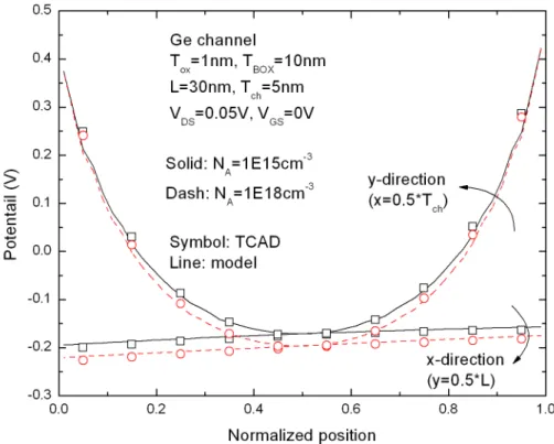
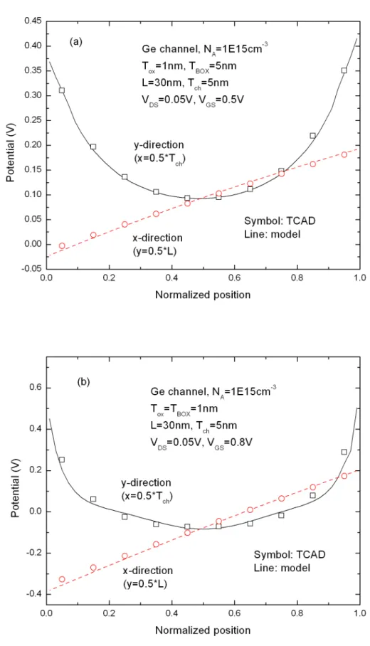
Comparisons between the compact parabolic form and series solution are shown in Fig 2.2. It shows that the reduced parabolic form is fairly accurate with L=30nm and 15nm and VDS=0.05V and 1V for Ge-channel devices. The curves of compact model in the y-direction are slightly discontinuous since we only reduce the channel
form instead of series solution.
2.3.2 Verification
We use Ge-channel devices in the model verification. The channel length (L) is 30nm and 15nm, the gate oxide thickness (T ) is 1nm, the channel thickness (ox T ) is ch
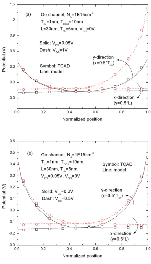
5nm and 10nm, the buried oxide thickness (TBOX ) is 1nm, 5nm and 10nm. The drain bias (VDS) is 0.05V and 1V and the back-gate bias (V ) is 0V, 0.2V, and 0.5V. The BS
channel doping concentration (N ) is 1x10A 15 cm-3 and 1x1018 cm-3. Besides, we use the heavily-doped (1x1020 cm-3) silicon substrate and treat it as ground plane.
Fig. 2.3 shows the potential distribution across half T and half ch L in the long- and short-channel devices and in the thin- and thick-channel thickness devices for model and TCAD results. It shows that our model is fairly accurate for various channel sizes. In Fig 2.4, our model is suitable for different channel doping concentrations (N ). In Fig 2.5, our model is also satisfactory for A TBOX =1nm and 5nm and implies that the model may be applied for double-gate (DG) devices when
BOX ox T
T . Fig 2.6 shows the potential distribution at high and low drain biases (VDS) and at different back-gate biases (V ). The model is also accurate compared with BS
TCAD simulations. The compact parabolic potential model shows excellent agreement with TCAD simulations for UTB devices.
2.4 Summary
We have developed a channel potential model for UTB MOSFETs under subthreshold region. Specifically, we propose a compact form of model instead of
series solution. To examine the accuracy of the compact parabolic model, we have carried out extensive verification for various L, T , ch N , A TBOX, VDS, and V . All BS
verification results show sufficient accuracy compared with TCAD simulations. The compact form not only makes the expression of potential model clear but also simplify the derivation of eigenenergy (E ) and eigenfuction (n ). That will be n
Fig. 2.1 Schematic sketch of the UTB structure investigated in this study.
T
BOX
Si substrate (Ground Plane)
D
S
x
y
L
T
ch
T
ox
T
BOX
Si substrate (Ground Plane)
D
S
x
y
L
T
ch
Buried Oxide
T
BOX
Si substrate (Ground Plane)
D
S
x
y
L
T
ch
T
ox
T
BOX
Si substrate (Ground Plane)
D
S
x
y
L
T
ch
Buried Oxide
Fig. 2.3 Potential distribution for UTB devices with (a) L=30nm and 15nm, and (b) T =5nm and 10nm using model and TCAD simulation. ch
Fig. 2.4 Potential distribution for UTB devices with N =1x10A 15 cm-3, and A
Fig. 2.5 Potential distribution for UTB devices with (a) TBOX=5nm, and (b) BOX
Chapter 3
Quantum-Confinement Model for
Ultra-Thin-Body MOSFETs with Thin BOX
Under Subthreshold Region
3.1 Introduction
With decreasing channel thickness, quantum-confinement effect may be significant [17]-[18] and may affect the electrostatic characteristics of ultra-thin-body (UTB) MOSFETs [19]. In this chapter, an analytical solution of the Schrödinger equation for UTB MOSFETs under subthreshold region is presented. Based on the parabolic channel potential model developed in Chapter 2, we derive the eigenenergy and eigenfunction of UTB devices. Therefore, the electron density in the channel considering quantum mechanism can be obtained by using the calculated eigenenergy and eigenfunction. Besides, we also discuss the impacts of channel material and surface orientation [20]-[21]. Quantum-mechanical effects on Si-, Ge-, and In0.53Ga0.47As-channel UTB devices will be assessed.
3.2 Model Derivation
The eigenenergy and eigenfunction of channel carriers are crucial to the quantum-mechanical effects, and they can be determined by solving the Schrödinger equation [3.6]. The schematic sketch of a UTB device has been shown in Fig 2.1. Because the direction of quantum confinement (x ) is perpendicular to the interface
between oxide and channel, for each cross-sections of y-direction, the Schrödinger equation for the UTB devices can be expressed as
) ( ) ( ) ( ) ( 2 * 2 2 x E x x E x x mx n C n nn (3.1)
, where E is the eigenenergy, n n
x is the corresponding wavefunction, is the reduced Plank constant, m*x the effective mass of electron perpendicular to the interface between oxide and channel, and EC
x is the conduction band edge.
In Chapter 2, we have proposed a compact form of the channel potential
1 0 2 2x a x a a x ch (equation (2.7)). Besides, the conduction band edge can be expressed as
C V g ch C N N q kT E x q x E ln 2 1 2 1 (3.2), where Eg is the band gap of channel material, N is the effective density of V
states in the conduction band, and N is the effective density of states in the valence C
band, respectively. Therefore, from equation (2.7) and equation (3.2), the conduction band edge can be expressed as
EC
x a2'x2 a1'xa0' (3.3), where a , '2 a , and 1' a0' are known values and can be obtained from the parabolic channel potential model presented in Chapter 2.
Using equation (3.3), equation (3.1) can be expressed as ( ) 2 2
2' 2 1' 0'
( ) 0 * 2 2 x a x a x a E m x x n n n (3.4) If we use the power series method and assume
0 ) ( i i i n x c x (3.5a), the coefficients c can be determined by the following recurrence relationship [22] i
2
0'
0 * 2 a E c m c x n (3.5b) 2
0'
1 1' 0
* 3 3 a E c a c m c x n (3.5c)
4
' 2 3 ' 1 2 ' 0 2 * 1 2 x n i i i i a E c a c a c i i m c , i4 (3.5d) The required boundary conditions can be described asn
x0
0 (3.6a) n
xTch
0 (3.6b)
ch T n x dx 0 2 1 ) ( (3.6c)From equation (3.6a), we know that c2 c0 0. Then c can be derived from 1
equation (3.6c) and the eigenenergy E can be obtained by equation (3.6b). Thus, n
the eigenfunction n(x) for UTB devices under subthreshold region can be derived. Generally, 60 terms in the summation of (3.5a) are needed to give sufficiently accurate results.
Using Fermi-Dirac statistics, the discrete nature of the quantized density of states reduces the integral over energy to a sum over bound state energies [23]. Besides, since we consider the quantum-confinement effect and possibly different types of valleys, the expression for the electron density then becomes [24]
n v n v n F d y x kT E y E kT m d y x n( , ) ,2 ln 1 exp , , , 2 (3.5), where is the type of valley, d is the degeneracy of the valley, md, is the effective density-of-state mass of the valley, and EF
y is the quasi-Fermi level in the channel along the y-direction.In equation (3.5), the exp
EF
y En.
kT
term is usually much smaller than 1 under subthreshold region. So we can further approximate the equation (3.5) as
kT y x E y E y x N y x n F C QM C ) , ( ) ( exp , ) , ( , (3.6a) with
n n n C d QM C x y kT E y x E m d kT y x N , , , 2 2 , , , exp ) , ( (3.6b)3.3 Verification and Discussion
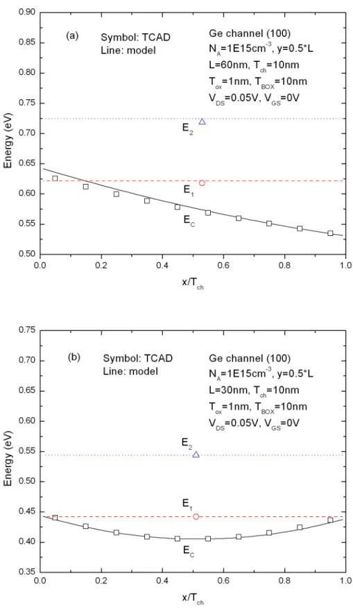
In Fig 3.1, we compare the conduction band edge and corresponding eigenenergies between long- and short-channel devices as T =10nm. It shows that ch
short-channel one. That is, the degree of quantization is affected by the conduction band edge with different channel length when T =10nm. ch
Fig 3.2 shows the calculated quantized n th eigenenergy (E ) in Ge-channel n
devices with various T . We can find that as ch T =5nm, ch
E2 E1
0.35eV is much larger than kT 0.026eV . From equation (3.6), it can be expected that the first eigenenergy (E ) will be dominant in the determination of the electron density when 1quantum-confinement effect is strong.
In Fig. 3.3, we show the square of the first eigenfunction (1 2) with T =5nm ch
and 10nm. Fig 3.4 shows the electron density across half L for the UTB devices. Although the square of the first eigenfunction with T =5nm is larger than the one ch
with T =10nm, the electron density with ch T =5nm is smaller than the one with ch
ch
T =10nm as shown in Fig 3.4. From equation (3.6), the T =5nmch UTB device is expected to have smaller electron density since it possess large
E 1 EC,min
as shown in Fig 3.2. Our quantum-mechanical model is fairly accurate compared with TCAD simulations.3.4 Various Channel Materials and Surface Orientations
Changing channel materials may improve device performance through the enhancement of carrier mobility. In this chapter, we will use Si, Ge, and In0.53Ga0.47As
as channel materials to examine our quantum-mechanical model. In addition, since Si and Ge have three common surface orientations (100), (110), and (111), we will discuss the impact of surface orientation considering quantum mechanism.
To consider quantum mechanism, the first thing is that different channel material or surface orientation may have different corresponding effective mass (m*x). The effective mass will determine the degree of quantization. The channel with lighter effective mass will have stronger quantum-mechanical effects. For a given surface orientation, Si or Ge may have two distinct effective masses with corresponding degeneracy (d ) and effective density-of-state mass ( md,). Table 3.1 shows m*x, d ,
and md, of the three channel materials considering various surface orientations [24]-[26].
In this work, we use our parabolic channel potential model for different channel materials. Then based on our quantum-mechanical model, we can use the parameters in Table 3.1 to solve the Schrödinger equation and to calculate the electron density considering the impact of surface orientation.
Fig 3.5 shows the channel potentials of Si and In0.53Ga0.47As, respectively. It can
be seen that our parabolic channel potential model is accurate. Fig. 3.6 shows the
E 1 EC,min
for Si with (100) and (110) surface orientations. Because theseorientations have two types of valley (two effective mass m*x ), there exists two
E 1 EC,min
. We can find that the difference between the two
E 1 EC,min
becomeslarge (>>kT 0.026eV) when T about 3nm. It means that the valley with smaller ch
E 1 EC,min
will determine the electron density in ultrathin T devices. Similarly, ch Fig 3.7 shows the
E E
for Ge with (110) and (111) surface orientations.When T about 5nm, the difference becomes obvious and hence we can treat the ch
valley with smaller
E 1 EC,min
as the dominant type for calculating the electron density. From Fig 3.6 and Fig 3.7, we can find that in ultrathin T devices ch(Tch 3nm for Si, Tch 5nm for Ge), the type of valley with heavier effective mass will determine the electron density.
Table 3.2 collects the critical effective masses (m*x,crit) which dominate the electron density. The table can help us understand what critical effective mass may affect the degree of quantization and corresponding electrostatic characteristics in ultrathin T devices. Fig 3.8 shows the dominant ch
E 1 EC,min
of Si-channel with (100) orientation, Ge-channel with (100) orientation, and In0.53Ga0.47As-channel UTBdevices, respectively. We can find that the In0.53Ga0.47As-channel UTB device has the
largest
E 1 EC,min
and thus experiences the strongest quantum-mechanical effects.Fig. 3.9 shows the square of the first eigenfunction (12 ) for Si- and In0.53Ga0.47As-channel UTB devices. Note that Si-channel UTB device with (100)
orientation has two types of 1 2. In Fig 3.10, we show the electron density for different channel materials in the UTB devices. It can be seen that for Si-channel UTB device with (100) orientation, the electron density of the dominant type of valley (2-fold valley) essentially determines the total electron density for the T =5nm ch
device. This supports our use of the critical effective mass to determine the degree of quantization.
3.5 Summary
In this chapter, we present the UTB MOSFET model considering quantum mechanism based on our previous parabolic channel potential model. Using the model, we can obtain eigenenergy, eigenfuction, and quantum electron density. Besides, we have demonstrated that
E 1 EC,min
will be the dominant term to determine the electron density, especially for ultrathin T devices. chWe have also discussed the impacts of different channel materials and surface orientations considering quantum mechanism. We find that the channel material which experiences the strongest quantum-mechanical effects has the lightest effective mass (m*x). We have constructed the table (Table 3.2) of the critical effective masses ( *
,crit
x
Fig. 3.1 The conduction band edge and corresponding eigenenergies for
ch
Fig. 3.2 The calculated quantized n th eigenenergy (E ) for the devices with n
Fig. 3.3 The square of the first eigenfunction (1 2) for T =5nm and 10nm in ch
the Ge-channel UTB devices.
Fig. 3.4 The electron density for T =5nm and 10nm in the Ge-channel UTB ch
Table 3.1 m*x, d , and md, of three channel materials considering surface
orientations. m is the free electron mass 0 9.111031kg. [24]-[26]
(100) (110) (111) * x m 0.916m 0 0.191m 0 0.316m 0 0.191m 0 0.259m 0 d 2 4 4 2 6 Si , d m 0.191m 0 0.418m 0 0.325m 0 0.418m 0 0.359m 0 * x m 0.117m 0 0.218m 0 0.08m 0 1.57m 0 0.0894m 0 d 4 2 2 1 3 Ge , d m 0.293m 0 0.215m 0 0.354m 0 0.08m 0 0.335m 0 * x m 0.041m 0 d 1 In0.53Ga0.47As , d m 0.041m 0
Fig. 3.5 The potential distribution of (a) Si-channel UTB device, and (b)
Fig. 3.6 The
E 1 EC,min
of Si-channel UTB devices with (a) (100) and (b) (110) surface orientations with model and TCAD results.Fig. 3.7 The
E 1 EC,min
of Ge-channel UTB devices with (a) (110) and (b) (111) surface orientations with model and TCAD results.Table 3.2 The critical m*x,crit of three channel materials considering surface orientations when quantum-mechanical effect is strong in ultrathin T ch
devices. (100) (110) (111) Si * ,crit x m 0.916m 0 0.316m 0 0.259m 0 Ge * ,crit x m 0.117m 0 0.218m 0 1.57m 0 In0.53Ga0.47As * ,crit x m 0.041m 0
Fig. 3.9 The square of the first eigenfunction (1 2) for (a) Si-channel with (100) surface orientation and (b) In0.53Ga0.47As-channel UTB devices.
Fig. 3.10 The electron density of Si-channel with (100) surface orientation and
Chapter 4
Impact of Quantum-Mechanical Effects
on Threshold-Voltage Roll-Off
in UTB GeOI MOSFETs
4.1 Introduction
Germanium as a channel material has been proposed to enable mobility scaling. However, its higher permittivity makes it very susceptible to Short Channel Effects (SCEs). To improve the electrostatic integrity, ultra-thin-Body (UTB) Germanium-On-Insulator (GeOI) MOSFET has been proposed as a promising device architecture and shows better control of SCEs than the bulk counterpart [27]-[28]. By scaling down the channel thickness, UTB GeOI MOSFETs can show comparable subthreshold swing as compared with the UTB SOI counterparts [29]. As the channel thickness scales down, the quantum-mechanical effect becomes more significant and its impact on the threshold-voltage (V ) roll-off in UTB SOI MOSFETs has been T
reported in [30]. However, the impact of quantum-mechanical effect on the V T
roll-off in UTB GeOI MOSFETs has rarely been examined.
In this chapter, we investigate the impact of quantum-mechanical effect on the T
V roll-off characteristics for UTB GeOI MOSFETs by the developed model in
4.2 UTB GeOI Devices and Simulation
The schematic cross section of UTB structure was shown in Fig 2.1. In this study, the gate oxide thickness (T ) is 1nm, the channel thickness (ox T ) ranges from 4nm to ch
10nm, the channel length (L) ranges from 2.4 to 10 times the T (proportional to ch
ch
T ), and the buried oxide thickness (TBOX) ranges from 10nm to 20nm. The channel doping concentration ( N ) is 1x10A 15cm-3. Besides, we use the heavily-doped (1x1020cm-3) silicon substrate and treat it as ground plane.
For UTB devices, our TCAD simulations self-consistently solves the Poisson’s equation (for channel potential) and 1-D Schrödinger equation (for eigenenergy and eigenfunction) at each slice perpendicular to the interface between oxide and channel. The process of the numerical calculations doesn’t have approximations. Therefore, the TCAD simulations can be exactly to assess quantum-mechanical effects for UTB GeOI devices.
In this study, the V is defined as the T VGS at which the average electron density of the cross-section at y ycrit exceeds the channel doping concentration. The ycrit stands for the position from the source of highest potential barrier for carrier flow. The ycrit is about L 2 for VDS=0.05V, and about L 3 for VDS=1V.
4.3 Results and Discussion
Fig. 4.1(a) and Fig 4.1(b) show the V roll-off of Ge- and Si-channel UTB T
devices with quantum-mechanical (QM) and classical (CL) considerations for ch
T =10nm and 5nm, respectively. In Fig 4.1(a), both the Ge- and Si-channel devices
with QM consideration show larger V roll-off than that with the CL one. However, T
in Fig 4.1(b), the Si-channel UTB MOSFET with QM consideration shows comparable V roll-off as compared with that using the CL one. The Ge-channel T
UTB MOSFET with QM consideration even shows smaller V roll-off than that T
with the CL one.
In [30], Y. Omura reported that the V roll-off would be increased by QM effect T
in UTB SOI MOSFETs. Their study used the simulator with density-gradient model (DGM) [31]-[32]. In our study, we can see the same trend of increased V roll-off in T
UTB SOI MOSFET. However, the V roll-off is suppressed by QM effect for UTB T
GeOI MOSFET with T =5nm. ch
Fig 4.1 can be explained by [33]-[34] QM
QM
T m
V
(4.1) , where m is the subthreshold slope factor, QM is the surface potential shift, and
QM T
V
is the V shift due to QM effects. In this work, we choose the peak of the T
channel potential at y ycrit cross-section as the reference potential. Therefore, the
E 1 EC,min
at y ycrit can stand for theQM
q when considering QM effects.
Fig 4.2 shows the
E 1 EC,min
for GeOI devices with T =10nm and 5nm. Fig ch4.2(a) shows that for GeOI devices with T =10nm, the ch
E 1 EC,min
of the long-channel (L6Tch) GeOI device is about 2.5
E 1 EC,min
the short-channel(L2.4Tch) one. In other words, the short-channel GeOI device with T =10nm ch
shows much smaller
E 1 EC,min
and thus smaller QM as compared with the long-channel one. This leads to larger V roll-off observed in Fig 4.1(a). On the Tother hand, Fig 4.2(b) shows that for the T =5nm GeOI devices, the ch QM of the long-channel (L6Tch) GeOI MOSFET is only ~1.3
E 1 EC,min
the short-channel ( L2.4Tch ) one. The m factor of the T =5nm short-channel GeOI device, chhowever, is about 2.5 the long-channel one. Therefore, for the T =5nm GeOI ch
devices, the VTQM of the short-channel device is larger than that of the long-channel one which results in the suppression of V roll-off observed in Fig 4.1(b). T
4.3.2 Surface Orientation
Fig 4.3 shows the V roll-off of three surface orientations in UTB GeOI T
MOSFET for T =4nm with QM and CL considerations. It can be seen that the ch V T
of the three orientations are (100)>(110)>(111). In Chapter 3, we have pointed out that the UTB GeOI device with T =4nm has a critical effective mass (ch *
,crit
x
m ). From Table 3.2, we can find that the critical effective masses of (100), (110), and (111) are 0.117m , 0.2180 m , and 1.570 m , respectively. This means that the degree of QM 0
effect is (100)>(110)>(111). It explains why the surface potential shifts (QM ) shown in Fig 4.3(b) are (100)>(110>(111). In other word, the (100) orientation GeOI devices have the largest VTQM and thus the largest V as shown in Fig 4.3(a). T
Fig 4.3(b) also shows the VTSCE of the three surface orientations. The VTSCE
VTSCE
mQM
long
mQM
short
VT,long VT,short
CL (4.2)Since the QM shown in Fig 4.3(b) is almost the same for long- and short-channel GeOI devices, the equation (4.2) can be approximated as
VTSCE QM
mlong mshort
VT,long VT,short
CL (4.3)Because the (100) orientation GeOI devices possess the largest QM, they have the smallest VTSCE. That is, the improvement of the V roll-off is the most significant T
for the (100) orientation GeOI devices. Note that
mlongmshort
is a negative number due to short channel effects (SCEs).4.3.3 Drain Bias and Buried Oxide Thickness
Fig 4.4(a) illustrates the V roll-off of the GeOI devices at T VDS=1V. Its worse SCEs shows lower V and larger T V roll-off than that with T VDS=0.05V. The VTQM
in the long-channel (L6Tch=30nm) GeOI devices are comparable between VDS=1V and 0.05V as shown in Fig 4.4(a). Fig. 4.4(b) shows that for the short-channel (L2.4Tch=12nm) devices, high-drain-bias GeOI device shows larger improvement of roll-off (~0.3V) than the low-drain-bias one (~0.1V). This is because the high-drain-bias device shows both larger
E 1 EC,min
(thus QM) and m factor than the low-drain-bias device as shown in Fig 4.5. For T =5nm GeOI devices, the chsuppression of the V roll-off caused by the QM effect is more significant at high T
Fig 4.6 shows the V roll-off of the T T =5nm GeOI devices with QM and CL ch
considerations for TBOX =20nm and 10nm. The long-channel (L6Tch=30nm) device with TBOX=20nm has comparable VTQM as compared with the TBOX=10nm device as shown in Fig 4.6(a). Fig 4.6(b) shows that at L=12nm, the GeOI device with
BOX
T =20nm shows larger improvement of roll-off than that with TBOX=10nm. This is because the TBOX=20nm device shows both larger
E 1 EC,min
(thus QM) andm factor than the TBOX =10nm device as shown in Fig 4.7. In other words, for the ch
T =5nm GeOI devices, the suppression of the V roll-off caused by the QM effect T
is more significant for TBOX =20nm than for TBOX=10nm. It should be noted that the GeOI device with TBOX =20nm shows larger V roll-off with CL consideration due T
to the drain field penetration through the buried oxide, which may be compensated by the more significant suppression of the V roll-off due to QM effects. Therefore, T
when considering QM effect, the Tch =5nm device with TBOX =20nm shows comparable V roll-off as compared with the T TBOX=10nm device as shown in Fig 4.6.
In Fig 4.8, we show the difference between VTQMlong and VTQMshort for devices design with different buried oxide thicknesses and drain biases. The long-channel GeOI device is L6Tch and the short-channel one is L2.4Tch. Then we make the intersections of the line
VTQMlongchannel VTQMshortchannel
=0 and the curves in Fig 4.8 and define the T locations of these intersections as the critical chchannel thicknesses (Tch,crit). Therefore, for GeOI devices with T >ch Tch,crit, the V T
show larger Tch,crit than those with low drain bias and thin TBOX .
4.4 Summary
We have investigated the impact of QM effects on the V roll-off in UTB GeOI T
MOSFETs. It shows two opposite trends for different ranges of T . For GeOI ch
devices with T >ch Tch,crit, the QM effect may increase the V roll-off. For GeOI T
devices with T <ch Tch,crit, the QM effect is found to suppress the V roll-off. We also T
find that the value of Tch,crit increases with drain bias and TBOX . This quantum-mechanical impact on short channel V roll-off should be considered when T
Fig. 4.1 The V roll-off of Ge- and Si-channel UTB devices with (a) T T =10nm ch