國立交通大學
電控工程研究所
博 士 論 文
鎖 相 迴 路 時 脈 抖 動 之 內 建 自 我 測 試
Built-In Self-Tests for Jitter Measurement of Phase-Locked Loops
研 究 生: 徐仁乾
指導教授: 蘇朝琴 教授
鎖 相 迴 路 之 時 脈 抖 動 內 建 自 我 測 試
Built-In Self-Tests for Jitter Measurement of Phase-Locked Loops
研 究 生:徐仁乾
Student:Jen-Chien Hsu
指導教授:蘇朝琴
Advisor:Chau-Chin Su
國 立 交 通 大 學
電控工程研究所
博 士 論 文
A DissertationSubmitted to Institute of Electrical Control Engineering College of Electrical Engineering
National Chiao Tung University in Partial Fulfillment of the Requirements
for the Degree of Doctor of Philosophy
in
Electrical Control Engineering May 2010
Hsinchu, Taiwan, Republic of China
鎖 相 迴 路 之 時 脈 抖 動 內 建 自 我 測 試
研 究 生:徐仁乾 指導教授:蘇朝琴 教授
國立交通大學電控工程研究所博士班
摘要
資料傳輸之品質受到時脈抖動之影響甚巨,然而針對時脈抖動的量產測試卻因成 本過高而難以實現,因此,時脈抖動的內建自我測試電路成為量產測試的一個解決方 案。時脈抖動的內建自我測試電路一般皆透過時間對數位轉換器來完成,將時脈抖動 轉換成為數位訊號,以低速數位訊號的方式提供量測機台進行量測,因此一個良好的 時間數位轉換器是內建自我測試的重要元件。在本論文中,我們提出了三種不同的時 間對數位轉換器以及內建自我測試電路,第一種是針對電荷幫浦式鎖相迴路的時脈抖 動量測所設計,它使用了新穎的高解析度時間對數位轉換器,可將受測電路本身的元 件重複利用做為時間對數位轉換器的一部份,因此縮小了額外的電路面積。量測結果 顯示其量測解析度可以達約兆分之一秒,而量測誤差小於百分之二十。第二種內建自 我測試電路是針對展頻時脈鎖相迴路所設計,它可分離展頻時脈的低頻調變訊號以及 高頻的時脈抖動訊號,同時建立一時脈抖動的估算方式,以驗證此電路的可行性。我 們實做了一個時脈頻率每秒十二億次、十個相位的鎖相迴路以及時脈抖動量測電路, 並比對量測結果與估算值,顯示量測誤差低於0.0026個單位區間。第三種內建自我測 試電路可量測資料與時脈回復電路的時脈抖動,並依據所量得之結果,估算資料之位 元誤差率,這種內建自我測試電路不需高解析度的延遲訊號線即可達到高精準度的量 測結果,它利用校正的機制和曲線對應的方式獲得高精準度。校正的機制是將壓控震 盪器切換至自由震盪模式,以機率統計的方式獲得時間對數位轉換器中延遲緩衝器的 延遲時間。此內建自我測試電路還可透過曲線對應的方式分離不同類別的時脈抖動, 以預估在位元誤差率為兆分之一的系統規格上的總時脈抖動大小。Built-In Self-Tests for Jitter Measurement of Phase-Locked Loops
Student:Jen-Chien Hsu Advisor:Chau-Chin Su
Institute of Electrical Control Engineering National Chiao Tung University
ABSTRACT
Signal quality of data transmission is significantly affected by clock jitter of Phase-Locked Loops (PLLs). However, production test for clock jitters is too expensive to implement. Built-In Self-Test (BIST) for clock jitter measurement becomes an alternative solution for production test. Basically, BIST methodologies are based on Time-to-Digital Converters (TDCs) which convert phase differences of a tested clock and a reference clock into low-speed digital signals for test equipments to measure. In this thesis, we proposed three kinds of TDCs and BIST circuits for different applications. The first one is designed for measuring clock jitter of charge-pump PLLs. The BIST is based on a novel high resolution TDC. Small area overhead is achieved by reusing the Voltage-Controlled Oscillator (VCO) and loop filter of the tested PLL as part of the TDC. The experiment result shows that the resolution is about one pico-second and the measurement error is smaller than 20%. The second BIST circuit is proposed for measuring timing jitter of Spread-Spectrum Clocks (SSCs). The BIST circuit can separate low-frequency phase drifting caused by frequency modulation and high-frequency jitter. Because of lack of dedicated instruments for SSC timing jitter measurement, a jitter estimation method is also developed for validating the feasibility of the BIST circuit. A 1.2GHz 10-phase Spread-Spectrum Clock Generator with a jitter measurement circuit is designed and fabricated. The experimental results show that the proposed built-in measurement approach has an error of less than 0.0026UI. The third BIST circuit is developed for testing the relative timing jitter of data and clock recovery circuits. This BIST circuit doesn’t need a high resolution delay line to achieve high accuracy measurement result, but uses calibration and curve-fitting algorithms. Calibration is done by switching the VCO of the tested PLL into free-running mode and using statistical theories to acquire accurate delay time of the delay buffers in the TDC. This BIST circuit also separates deterministic jitter and random jitter by adopting the bathtub curve-fitting algorithm and estimates total jitter at bit-error rate=10-12 level.
誌謝
首先我要感謝法輪大法(法輪功)讓我恢復健康的身體。我在就讀研
究所前,不幸罹患一種稱為「僵直性脊椎炎」的免疫系統疾病,這種重
大疾病一旦發病即可免除兵役,且發展到後來必須長期靠類固醇藥物控
制,嚴重時將長期臥病在床。所幸我在發病初期,就開始接觸並修煉法
輪大法。法輪大法是一種「性命雙修」的功法,除了強調心性的提高外,
還可以使修煉者身體得到健康。因為學煉法輪大法,我的身體漸漸得到
康復,所以如今才能過著正常人的生活,且順利完成研究所的學業。
接著我要感謝指導老師蘇朝琴教授,在跟隨蘇老師做研究的過程中,
我學習到一種做學問的方式,蘇老師要求我們凡是從基本的物理意義上
去看問題,不要被複雜的公式所迷惑。養成這種習慣之後,往往對問題
的認識能更為深入。還有蘇老師常說:
「模擬軟體是用來驗證自己的想法
的,並不是用來指導做研究的。」我覺得這點也讓我受益良多,所以使
用模擬軟體前,我都會先想想自己能否預期將有什麼樣的模擬結果。
我還要感謝蘇老師在為人處事上給我的指正,在我畢業前,他語重心
長的告訴我,不要經常流露出對別人輕蔑的態度。我仔細想想,確實如
此,但很少有人指出我的缺點,因此我要感謝他給我的指正,我認為這
對我未來的人生有很大的幫助。
我還要感謝我的父母、兩個哥哥以及妻子長期以來在經濟上和精神上
的支持,由於他們無條件的供應學費並且鼓勵我、體諒我,我才能夠安
心的完成博士班的學業。
最後我要感謝我的同窗好友和助理,阿亮學長、煜輝學長、丸子、盈
杰、豐文、鴻文、能哥、教主、楙軒、洲銘、于昇、家齊、阿達、信文、
孔哥、小馬、瑛佑、智琦、忠傑、泓瑋、妍儒、俊秀、依萍、方董、修
銘、雅雯、英廷、冠羽、柏成、小冠、匡良、宗諭、順閔、上容、議賢、
威翔、彥呈、成宇、建錫、祥哥、村鑫、俊銘、朋哥、碩廷、汝敏、鈞
藝、哲瑋、博祥、群育、子俞、雅婷、挺毅,由於他們的陪伴使我度過
了愉快的研究所生涯。
Table of Contents
摘要 iii ABSTRACT iv
誌謝 v
Table of Contents... vi
List of Figures viii List of Tables xi Chapter 1 Introduction ... 1
1.1. Jitter Definition ... 1
1.2. BIST for Measuring PLL Jitter ... 2
1.3. BIST for Measuring SSC Jitter ... 10
1.4. BIST for Measuring CDR Jitter... 12
1.5. Organization of the Dissertation ... 14
Chapter 2 BIST for Charge-Pump Phase-Locked Loops ... 15
2.1. Time-to-Digital Converter ... 15 2.2. Circuit Description... 19 2.2.1. TDC... 20 2.2.2. Control Unit ... 23 2.2.3. Calibration... 24 2.3. Experimental Results ... 26
Chapter 3 BIST for Spread-Spectrum Clocks ... 37
3.1. BIST Methodology Overview... 37
3.2. SSC Jitter Estimation ... 41
3.2.1. Derivation of HVCO(s) and HΣΔ(s) ... 43
3.2.2. Derivation of ΣΔ Φ S ... 46 3.2.3. Derivation of VCO Φ S ... 49 3.3. Experimental Results ... 51
Chapter 4 BIST for Clock and Data Recovery Circuits... 61
4.1. Proposed BIST circuit... 61
4.1.1. Timing Capture Scheme... 61
4.1.2. Bathtub Curve-Fitting ... 62
4.1.3. Circuit Description ... 64
4.2. Calibration ... 66
4.3. BIST Operation Steps ... 67
4.4. Simulation Results ... 68
Chapter 5 Conclusions and Future Work... 71
5.2. Future Work ... 72 References 74
VITA 80
List of Figures
Fig. 1 Jitter definitions... 1
Fig. 2 Delay line TDC. ... 2
Fig. 3 Delay line with fine resolution... 3
Fig. 4 Vernier Delay Line. ... 3
Fig. 5 Ring Type Vernier Delay Line... 4
Fig. 6 Sampling Offset TDC... 4
Fig. 7 Pulse-Shrinking Delay Line. ... 5
Fig. 8 Pulse-Shrinking Delay Line Ring Type... 5
Fig. 9 Local Passive Interpolation. ... 6
Fig. 10 Analog-to-Digital Converter for Jitter Measurement... 6
Fig. 11 Time amplifier. ... 7
Fig. 12 Dual-slope ADC for time amplifying... 7
Fig. 13 Time-to-Voltage Converter for average jitter measurement... 8
Fig. 14 Time-to-Voltage Converter with flash ADC... 8
Fig. 15 Hybrid of TVC and delay line... 9
Fig. 16 Under-sampling-based technique... 9
Fig. 17 (a) Modulation profile. (b) Power spectral density of Spread-Spectrum Clock... 10
Fig. 18 Jitter measurement methodology... 11
Fig. 19 Tranceiver architecture and BIST... 12
Fig. 20 Clock Recovery circuit and BIST... 12
Fig. 21 Bathtub curve characterized by the jitter of RJ=0.2UI and DJ=0.04UI... 13
Fig. 22 Time-to-Digital Converter... 15
Fig. 23 Initial control voltage of VCO. ... 18
Fig. 24 Proposed BIST circuit. ... 20
Fig. 25 Modified Phase-Frequency Detector... 21
Fig. 26 PFD2 circuit design... 22
Fig. 27 Timing behavior of PFD2... 22
Fig. 28 Timing behavior of circuit with DL1. ... 22
Fig. 29 Loop Filter is modeled as a capacitor... 22
Fig. 30 Timing diagram of Control Unit. ... 23
Fig. 31 Divider with an output pulse width that equals the period of VCO... 24
Fig. 33 Timing behavior of calibration... 25
Fig. 34 Chip photograph... 29
Fig. 35 Measurement equipment. ... 29
Fig. 36 Injecting noise into the power line. ... 30
Fig. 37 PLL DIV output clock jitter with 40mV p-p random noise. ... 30
Fig. 38 Histogram of BIST output in calibration mode with 40mV p-p random noise... 30
Fig. 39 Histogram of BIST output in test mode with 40mV p-p random noise. ... 31
Fig. 40 PLL divider output jitter by oscilloscope (40mV p-p 10MHz sinusoidal)... 31
Fig. 41 Histogram of BIST output in calibration mode (40mVp-p 10MHz sinusoidal). .... 32
Fig. 42 Histogram of BIST output data in test mode (40mVp-p 10MHz sinusoidal). ... 32
Fig. 43 RMS jitter measured using oscilloscope and the BIST circuit... 33
Fig. 44 Peak-to-peak jitter measured using oscilloscope and the BIST circuit... 33
Fig. 45 Proposed BIST methodology. ... 37
Fig. 46 Multi-Phase Phase Detector. ... 38
Fig. 47 Timing diagram of the MPD. ... 39
Fig. 48 BIST methodology model. ... 40
Fig. 49 Noise model of the SSCG... 42
Fig. 50 The SSCG structure with multi-phase selection. ... 47
Fig. 51 Jitter estimation and calibration flow. ... 49
Fig. 52 Chip photograph... 50
Fig. 53 PSD of the non-SSC clock and SSC measured using a spectrum analyzer. ... 50
Fig. 54 Phase shift detector output signal... 51
Fig. 55 Accumulator output signal. ... 52
Fig. 56 Modulation profile of the SSCG... 52
Fig. 57 Phase noise of non-SSC clocks with natural frequencies of 0.4MHz and 0.9MHz.53 Fig. 58 Phase noise of non-SSC clocks with natural frequencies of 0.4MHz and 2.2MHz.53 Fig. 59 Curve-fitting procedure for calibration of transfer functions... 54
Fig. 60 Non-SSC jitter with a natural frequency of 400kHz. ... 56
Fig. 61 Theoretical PSDs of the jitter and phase quantization noise... 56
Fig. 62 Theoretical and measured PSDs of jitters (fn= 0.4MHz)... 57
Fig. 63 Theoretical and measured PSDs of jitters (fn= 0.9MHz)... 57
Fig. 64 Theoretical and measured PSDs of jitters (fn= 2.2MHz)... 58
Fig. 66 Jitter RMS value, BIST vs. estimation results ... 60
Fig. 67 Timing capture scheme of BIST and error detection ... 62
Fig. 68 Measured data points and bathtub curve... 63
Fig. 69 Proposed BIST circuit. ... 64
Fig. 70 PDF of phase difference between NRZ data and free running VCO clock ... 66
Fig. 71 System level simulation flow of BIST ... 68
List of Tables
Table 1 Jitter measured using oscilloscope and the BIST circuit. ... 34
Table 2 PLL specifications. ... 35
Table 3 BIST specifications... 35
Table 4 Performance Comparison. ... 36
Table 5 Comparison of measured and estimated RMS jitter. ... 59
Table 6 Parameters of BIST... 70
Table 7 Simulation results. ... 70
Chapter 1
Introduction
1.1. Jitter Definition
Phase-Locked Loops (PLLs) are extensively employed as clocking signal sources in digital and mixed-signal circuits. In high speed link applications, jitter represents the problem of data uncertainty. Thus, clock jitter of PLLs is one of the most important properties to be measured.
Clock jitter is defined as the timing deviation of the tested clock from the ideal clock. Jitter can be categorized into several types according to different definitions. Fig. 1 illustrates three jitter definitions: period jitter, cycle-to-cycle jitter, and timing jitter. Period jitter is defined as the difference between the tested clock period and the reference clock period. Cycle-to-cycle jitter is defined as the difference between the current period and the previous one of the tested clock. Timing jitter, also known as long-term jitter, is the timing difference between the tested clock edge and reference clock edge. In general, timing jitter is more useful for Bit-Error Rate (BER) estimation because a bit-error occurs when the
Ref Clock Tested Clock Timing jitter 0 T 0 T Period Jitter 1 T T2 ) ( 0 0 2 T T T T n− = − = 3 T
Cycle to cycle jitter
) ( 1 1 2 − − = − = n n T T T T 0 1T nT n i− ∑ = 0 T T0
timing of the tested clock edge deviates from its ideal position for an intolerable magnitude.
Jitter can also be categorized by its noise sources such as Deterministic Jitter (DJ) and Random Jitter (RJ). The amplitude of DJ is bounded, since the noise sources are the Duty-Cycle Distortion (DCD), Inter-Symbol Interference (ISI), switching noise of the power supply, and other noise sources whose values can be estimated. RJ is unbounded, since the noise sources are thermal noise, flicker noise, and other noises induced by electronic movements. Total Jitter (TJ) is the combination of DJ and RJ. Besides, jitter is usually presented in two statistical forms: RMS jitter is the root-means square values of the jitter, and peak-to-peak jitter is the maximal value of the jitter.
1.2. BIST for Measuring PLL Jitter
As clocks speeds reach GHz in recent years, measuring clock jitter using external high speed test equipments becomes increasingly expensive. To reduce testing cost, a Built-In Self-Test (BIST) method is considered as a feasible alternative. The most common method of BIST is based on Time-to-Digital Converters (TDCs). Several state-of-the-arts of BIST and TDC approaches are introduced as follows:
1. Delay line [1]-[10]: The method is based on a delay line to obtain a cumulative
Frequency Difference PFD CP&LF VCO Divider Adjustable Delay Constant Delay clk D Q Latch Counter R.O. Freq. Counter fref
Enable ring osc.
Calibration
distribution function of jitter, as shown in Fig. 2. This is the simplest and straightforward method to implement TDCs. By adjusting the delay line, the timing differences of the reference and tested clock edges are measured. The calibration of the delay buffer is done by connecting two ends of the delay buffer to form an oscillator, so the delay time can be estimated based on its oscillation frequency. Various calibration techniques are also developed to improve the accuracy of the delay-line-based approaches [11]-[13].
A digitally controlled delay line has a coarse resolution of about one gate delay. Therefore, a voltage-controlled delay line is used to improve the delay line resolution [7]. As shown in Fig. 3. The resolution can be as good as sub-picosecond using accurate analog bias voltage.
2. Vernier Delay Line [14]-[20]: The Vernier Delay Line is also developed to increase
Ref clock Data Control Circuit Vctrl R.O. Counter
Latch Latch Counter
Fig. 3 Delay line with fine resolution.
D Q Coun te r 1 τ 2 τ D Q 1 τ 2 τ D Q 1 τ 2 τ Data Clk Vdata Vclk Count e r Count e r
the TDC resolution. As shown in Fig. 4, the resolution is determined by the delay difference of two delay buffers; thus the resolution is improved. However, the area overhead is large and accurate analog bias voltages are also required.
3. Ring Type Vernier Delay Line [21]-[25]: The Ring Type Vernier Delay Line (also called Component-Invariant Vernier Delay Line) is developed to solve the problems of mismatch and large area overhead of the Vernier Delay Line. As shown in Fig. 5, a delay buffer is connected as a ring oscillator to replace all the other delay buffers of the Vernier Delay Line. Both Vernier Delay Line and Ring Type Vernier Delay Line require an additional Digital-to-Analog Converter (DAC) to generate accurate analog control voltages to fine-tune the delay time of each delay line.
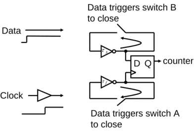
Data triggers switch A to close
Data triggers switch B to close Data Clock D Q s τ f τ counter
Fig. 5 Ring Type Vernier Delay Line.
D Q Counter D Q D Q Data Clk Count e r Count e r 1 os t tos2 tosn
4. Sampling Offset TDC [26]-[28]: Sampling Offset TDC uses non-ideal DFFs as comparators to produce different sampling time offset to mimic the function of Vernier Delay Lines. As shown in Fig. 6, the sampling time of each DFF is different due to different sizing of the transistors of the DFF. The merit of this approach is that delay buffers and its analog bias voltages are not needed. However, each DFF requires careful sizing and the linearity is not guaranteed.
5. Pulse-Shrinking Delay Line [29]: As shown in Fig. 7, Pulse-Shrinking Delay Line takes advantage of the difference between the propagation delay of the charge and discharge paths of the delay buffers to quantify timing jitter, so the resolution is smaller than one gate delay. However, the propagation delay of the charge and discharge paths should be carefully designed since those paths are sensitive to process variation.
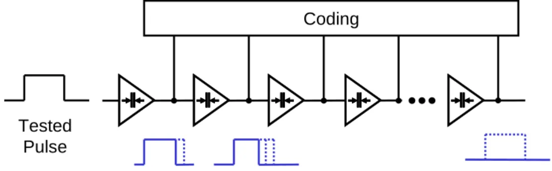
6. Ring Type Pulse-Shrinking Delay Line [30][31]: As shown in Fig. 8, the Ring Type Pulse-Shrinking Delay Line (also called Cyclic Pulse Width Modulator) uses the Pulse-Shrinking Delay Element to build a cyclic loop, so the area overhead is smaller than
Coding
Tested Pulse
Fig. 7 Pulse-Shrinking Delay Line.
Tested Pulse RST
that of the Pulse-Shrinking Delay Line.
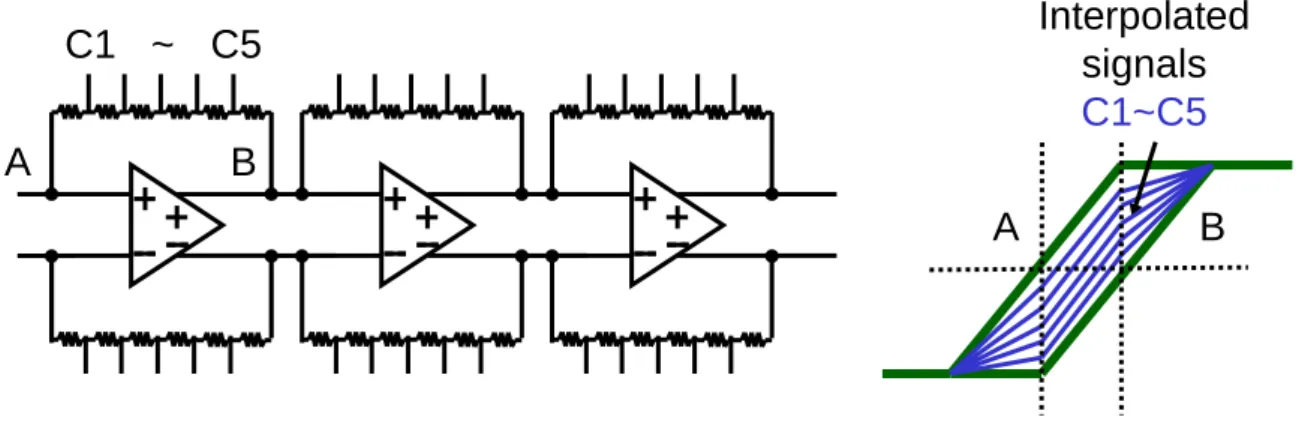
7. Local Passive Interpolation [32][33]: The coarse resolution of the delay line approach is subdivided by a passive interpolation technique. As shown in Fig. 9, this method uses passive components for phase interpolation and provides a time domain resolution of 4.7ps. This approach has the merit of monotonic phases, but the shortcoming is that the layout of the passive components should be carefully designed, and more comparators and counters are needed.
8. Analog-to-Digital Converter [34]: As shown in Fig. 10, the Analog-to-Digital Converter (ADC) converts clock jitter into digital codes by applying a sine wave to the ADC input and the tested signal to the ADC clocking input. This approach exhibits high resolution and short test time, but it requires the generation of a sinusoidal waveform with high spectral purity and requires the use of a high-performance ADC.
Interpolated
signals
C1~C5
A
B
B
A
C1
~
C5
Fig. 9 Local Passive Interpolation.
Sin wave
Narrow-band Bandpass
Filter
ADC Digital Code
Tested signal Timing distribution Sin wave
9. Time amplifier [35]-[39]: As shown in Fig. 11, the method is developed to improve the resolution of TDC by adding a time amplifier to the input of poor-resolution TDCs. This approach can enhance the resolution of TDCs to 2 pico-second [35][36]. Another type of time amplifier is also presented in [37]. Fig. 12 shows dual-slope ADC designed for amplifying the pulse width of the tested signal. The shortcoming of these time amplifiers is that they are sensitive to noise because of their gentle signal slopes.
10. Time-to-Voltage Converter [40]-[46]: The Time-to-Voltage Converter (TVC) approach converts phase difference into voltage using a charging pump and a capacitor. The voltage is further converted into a digital code using a specially designed ADC. As shown in Fig. 13, this approach uses its analog characteristics to achieve high resolution [40]. However, the shortcomings of this approach are that the measurement sensitivity of the TDC is limited by the dead-zone of the phase detector, and the constant phase error between the reference clock and the tested clock induces measurement error. Additionally,
1 in φ 1 out φ 2 in φ φout2 1 in φ 2 in φ 1 out φ 2 out φ
Fig. 11 Time amplifier.
N*I I T N*T Comparator Counter N*T
the BIST circuit measures average jitter but not RMS jitter. Fig. 14 shows another TVC with a flash ADC converting voltage signals into digital codes. This approach has fast conversion speed but large area overhead is a problem due to the need of a high resolution flash ADC.
11. Hybrid of TVC and delay line [47]-[49]: This approach adopts both delay line and TVC to perform a jitter measurement without a reference clock. As shown in Fig. 15, it uses a delay line to measure the period jitter and then uses a TVC to accumulate the period jitter to have timing jitter. Although some similar works for omitting reference clocks have been done [3][8][9][20][25], the novelty of this hybrid approach is that it can measure timing jitter instead of period jitter, even without a reference clock. However, a very accurate delay buffer to extract period jitter is needed.
PFD CP LF VCO DIV D Q QB Ic Id Vinp Vbase DN UP Vref
Fig. 13 Time-to-Voltage Converter for average jitter measurement.
Flash ADC
Pulse
Voltage
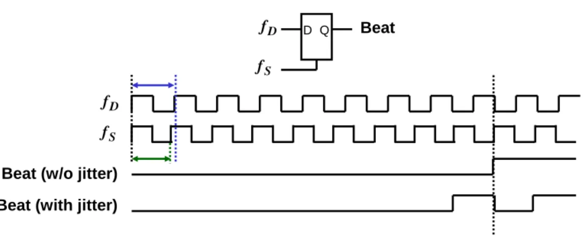
12. Under-sampling-based technique [50]-[53]: As shown in Fig. 16, the tested clock is sampled by a slightly lower frequency clock, so a phase resolution is determined by the frequency difference between the tested clock and sampling clock. The advantage of this approach is that only a D flip-flop (DFF) is needed, so it can be synthesizable, but the disadvantage is that it requires two oscillators on PCB board which are fine-tuned to have oscillation frequencies with very slight difference.
Because the BIST approach with TVC has the potential of high resolution, but has large hardware overhead. The fist part of this work tries to modify the TVC approach by developing a high-resolution and small-area circuit. A high-resolution TVC is achieved by adopting a voltage-to-frequency conversion, i.e. a Voltage-Controlled Oscillator (VCO). Small area overhead is achieved by using the VCO of the tested circuit as part of the BIST circuit.
Charge Pump Voltage meter
PFD Delay
Tested Clock
Period Jitter Timing Jitter
Accumulation
Fig. 15 Hybrid of TVC and delay line.
D Q Beat D f S f D f S f
Beat (w/o jitter) Beat (with jitter)
1.3. BIST for Measuring SSC Jitter
The second part of this work is for jitter measurement of Spread-Spectrum Clocks (SSCs). Conventionally, BIST circuits for jitter measurement use Time-to-Digital converters (TDCs) to compare the phase difference between a generated clock and reference clock. The resolution of TDCs determines the accuracy of jitter measurement results. Unfortunately, a Spread-Spectrum Clock (SSC) has a frequency deviation due to a predefined modulation profile that attenuates peak power, as shown in Fig. 17. The phase variation of the SSC includes jitter and the phase drifting resulting from the designed frequency deviation. Separating those by using conventional TDC approaches or external instruments is difficult.
Although the phase drifting caused by the frequency modulation is a deterministic jitter, and the deterministic jitter and random jitter separation algorithm [54] can be used to separate jitter. However, if a phase drifting is larger than 1UI, the histogram becomes flat and meaningless. It happens for most SSCs. Furthermore, even if the deterministic jitter can be separated from the random jitter, the deterministic jitter induced by the tested Phase-Locked Loop (PLL) and the SSC phase drifting cannot be separated because they all are deterministic jitter. More importantly, the SSC phase drifting is a low-frequency signal that is not crucial for receivers to recover the data, but other high-frequency deterministic
nom f nom f ) 1 ( −δ m f / 1 Time Frequency Non-SSC Frequency Deviation Peak Reduction SSC (a) (b)
jitter is important, so separating different types of deterministic jitter is necessary.
Timing jitter of SSCs cannot be measured using traditional approaches, thus spectrum analyzers are frequently used to measure the power spectrum of SSCs for roughly estimating the signal quality. The self-trigger function of oscilloscopes is typically utilized to measure period jitter. However, period jitter is not useful for estimating BER.
Because the timing jitter is more appropriate for BER estimation than the period jitter [57]-[60]. Serial ATA (SATA) develops a timing jitter measurement methodology [55] as shown in Fig. 18. Jitter is defined as the time difference between a recovered clock and a data edge. The clock recovery circuit has a low-pass transfer function with a corner frequency of fBAUD/500 or fBAUD /1667 depending on different applications, where
BAUD
f is the nominal rate of data through the channel. However, the jitter includes the transmitted jitter and the jitter induced by the clock recovery circuit if an ideal recovery circuit is not used. Moreover, an additional clock recovery circuit is needed when using this methodology.
In the second part of this work, a BIST methodology for measuring timing jitter and the modulation profile of SSCs is proposed. The measured results are validated by the
c f 1667 / 500 / BAUD c BAUD c f f f f = = Clock Recovery Circuit Serial Data Recovered Clock Recovered Data Frequency Mag n it u de dB Clock Recovery Bandwidth DFF c f 1667 / 500 / BAUD c BAUD c f f f f = = Clock Recovery Circuit Serial Data Recovered Clock Recovered Data Frequency Mag n it u de dB Clock Recovery Bandwidth DFF Clock Recovery Circuit Serial Data Recovered Clock Recovered Data Frequency Mag n it u de dB Clock Recovery Bandwidth DFF DFF
estimation based on the measured results using external instruments.
1.4. BIST for Measuring CDR Jitter
The third part of this work is to measure the TJ and BER of the clock and data recovery circuits using an accurate BIST circuit and jitter decomposition algorithm. Conventionally, oscilloscopes and time interval analyzers provide some convenient jitter decomposition algorithms to estimate BER. In this work, a combination of jitter decomposition and jitter measurement is proposed to implement a BER testing by BIST circuits. A calibration method is also proposed to improve the accuracy of the TDC.
Most state-of-the-arts of the jitter BISTs are measuring the clock jitter and jitter histogram. In this work, a method is proposed to measure relative timing jitter between received NRZ data and recovered clock of CDR and then estimate the peak-to-peak jitter at bit error rate (BER) of 10-12 level. Fig. 19 and Fig. 20 show the application of the BIST. The relative timing jitter between the received data and recovered clock of CDR represents the timing performance of the communication system, including transmitter, channel, and
Serializer DeSerializer
Driver
Channel
Receiver
CDR
BIST for jitter measurement Serializer DeSerializer Driver Channel Receiver CDR
BIST for jitter measurement
Fig. 19 Tranceiver architecture and BIST.
Phase Detector NRZ Data Loop Filter VCO Recovered Clock BIST Phase Detector NRZ Data Loop Filter VCO Recovered Clock BIST
receiver. Thus, the relative timing jitter helps to estimate the BER [56].
Because directly measuring the peak-to-peak jitter at the 10-12 BER level consumes a lot of time, the techniques of jitter decomposition are commonly used. TJ in a typical system is the combination of DJ and RJ. DJ has a non-Gaussian PDF and bounded peak-to-peak amplitude. RJ is characterized by a Gaussian distribution and assumed to be unbounded.
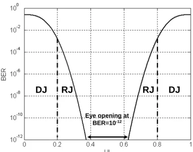
Some techniques for decomposing the TJ are presented in [54]. For example, Oscilloscopes and Time Interval Analyzers provide some convenient jitter decomposition algorithm, such as TailFit algorithm created by Wavecrest. A bit error rate tester (BERT) utilizes scan/bathtub curve for jitter decomposition, as shown in Fig. 21.
In this work, a new definition of a bit-error is given and the data provided for bathtub curve-fitting is obtained by BIST circuit instead of BER tester. Additionally, the hardware overhead in this work is small because only several data points of jitter magnitude is measured instead of a jitter histogram, which needs a high resolution TDC for depicting the whole scale of the jitter amplitude.
DJ RJ DJ Eye opening at BER=10-12 RJ DJ RJ DJ Eye opening at BER=10-12 RJ
1.5. Organization of the Dissertation
The dissertation is organized as follows. Chapter 1 introduces the motivation of this work and the dissertation organization. Chapter 2 presents the BIST circuit for measuring jitter of charge-pump PLLs. Chapter 3 presents the BIST circuit for measuring timing jitter of Spread-Spectrum Clock Generators (SSCGs) and the jitter estimation method for validating the BIST circuit. Chapter 4 describes the BER estimation method using a BIST circuit and the calibration method to improve the accuracy of the BIST circuit. Chapter 5 concludes this work.
Chapter 2
BIST for Charge-Pump Phase-Locked
Loops
2.1. Time-to-Digital Converter
The use of TDC to measure jitter is the concept that underlies BIST circuits. TDC detects each phase difference between the reference clock and the tested clock to obtain the jitter histogram. As shown in Fig. 22, the proposed TDC is composed of Phase-Frequency Detector (PFD), Charge Pump (CP), Capacitor (C), VCO, Divider (DIV) and Counter.
Two clocks CLK1 and CLK2 with a phase difference, Δ , is input to PFD. The T phase difference is detected using PFD only once and the PFD is disabled before the next clock edge arrives. CP and Capacitor convert the phase difference into a voltage variation
V Δ . , T C I V = p Δ Δ (1)
where I is the current magnitude of CP and C is the capacitance of Capacitor. p
PFD VCO Counter
CLK1 CLK2
RST
DIV Phase Difference
C CP PFD VCO Counter CLK1 CLK2 RST
DIV Phase Difference
C CP
The frequency of VCO is changed from fVCO0 to fVCO1. The frequency variation f
Δ of the DIV output is
, 0 1 N V K N f f
f = VCO − VCO = VCOΔ
Δ (2)
where N is the division ratio of DIV and KVCO is the gain of VCO.
DIV slows down the clock frequency of VCO N times for the low-speed counter to count. Counter counts the DIV clock edges in time, TC, to measure the frequency. Counter value, N , and DIV frequency, C fDIV , are related as follows.
.
C DIV C f T
N = (3)
If N is the count in C1 T when the DIV frequency is C fDIV1, and N is the count C0 when the DIV frequency is fDIV0, then the frequency variation and count difference, ΔN, are related as follows.
. ) ( 1 0 0 1 C DIV DIV C C C N f f T fT N N = − = − =Δ Δ (4)
Equations (1), (2) and (4) yield the relationship between the count difference, ΔN, and the phase difference, Δ . T . N T I K NC T C P VCO Δ = Δ (5)
The count difference yields the phase difference. One count difference denotes that a phase difference of kRES has been detected, where the coefficient, kRES , represents the
measurement resolution. ). ps/count ( C P VCO RES T I K NC N T k = Δ Δ = (6)
Due to the process variation, the gain of VCO, current magnitude of CP and capacitance of the capacitors of the fabricated chip will not be as the same as the ones from
the simulation results. To calibrate the TDC and obtain the accurate coefficient, kRES, of the fabricated chip, a pulse with the known pulse width TΔ is input to CP. The count difference ΔN is obtained and the accurate coefficient is calculated.
The proposed TDC measures small phase differences between two clocks because the dead-zone of PFD is zero. The commonly-used zero dead-zone PFD is implemented using two edge-triggered, resettable D flipflops. The UP and DN signals of the PFD are simultaneously high for a short time. Even if the phase difference of two inputs are nearly zero, the UP and DN signals still have short pulses to turn on the transistors of CP. The difference between their pulse widths represents the phase difference. Thus zero dead-zone is achieved.
A constant phase offset between CLK1 and CLK2 must be considered. If there is current mismatch between the charging and discharging path of CP, the PLL will compensate the mismatch automatically by keeping the pulse widths of these two short pulses different, so the constant phase offset between CLKA and CLKB occurs. The phase offset can also be measured and separated from the jitter by observing the histogram of the phase differences. The mean in the histogram represents the phase offset error and the variance represents the jitter.
The parameters of CP and Capacitor should be carefully designed to have a proper detection range. If the current is too large and the capacitance is too small, the voltage variation will fall out of the VCO control voltage range. If the current is too small and the capacitance is too large, then the voltage variation will be too small and then the noise on the node of Capacitor will induce more measurement error.
The value, T , is the parameter that determines the measurement resolution. For C longer T , the measurement resolution is higher, but the effect of the leakage current C increases and the test time also increases.
Capacitor and VCO have a large area and dominate the area overhead of the BIST circuit. Fortunately, the loop filter, the VCO and the divider of the tested PLL can be adopted as part of the TDC. Therefore, the area overhead is reduced. PFD and Counter only comprise several logic gates; therefore, the total area is small.
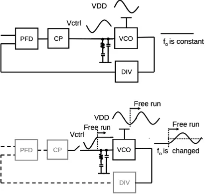
One noise source may deteriorate the accuracy of this approach. The TDC utilizes the VCO and the loop filter of the tested PLL as part of the circuit, but the initial value of the VCO control voltage is not constant due to power supply noise and a PLL tracking ability. Fig. 23 shows the timing diagram of a VCO in a PLL and the noise of the power supply. Assume the frequency of the noise is much lower than the loop bandwidth of the PLL. A phenomenon is observed that the voltage of the loop filter is varying in the opposite phase of the power supply noise to cancel the effect of the noise and keeping the frequency of VCO constant. It is reasonable because the frequency of the supply noise is much lower than the loop bandwidth so the PLL can keep the frequency of the VCO constant and lock the phase of the reference clock. If the loop of PLL is opened at a particular time, the
VCO DIV CP PFD f o is constant VDD Vctrl VCO DIV CP PFD f o is constant VDD Vctrl VCO DIV CP PFD VDD Vctrl Free run fo is changed Free run Free run VCO DIV CP PFD VDD Vctrl Free run fo is changed Free run Free run
voltage of the loop filter is kept in a particular value by the capacitors of the loop filter at that moment. This value becomes the initial value of the VCO control voltage of the TDC. However, this value is determined by the power supply noise voltage at the moment when the loop is opened, so the value is not predictable.
The frequency deviation of the VCO caused by the noise is derived as the power supply noise multiplying the VCO power supply gain, KVCO2. The VCO power supply gain is defined as VCO frequency variation over power supply variation. For example, the peak value of power supply noise is 2mV and the VCO power supply gain is 200MHz/V. The maximum frequency deviation of the VCO is 0.4MHz and the maximum frequency deviation of the divider output is 25kHz, if the division ratio is 16. After counting time 200μs, the count of the counter deviates from its ideal value for 25k⋅200μ =5. Then 5 is multiplied by the measurement resolution of 1ps/count to be 5ps. So the measurement error is 5ps. The measurement error, ΔT1, is derived as follows.
, 2 2 1 P VCO VCO n RES C VCO n I K NC K V k T K V T = = Δ (7)
where V is the power supply noise. n
The only parameter which can be adjusted to suppress the measurement error is the current of CP, so the current should be designed as large as possible. If the complete avoidance of this noise source is desired, an additional capacitor instead of the loop filter should be used to generate constant initial control voltage of VCO.
2.2. Circuit Description
As shown in Fig. 24, the BIST circuit comprises three main parts - TDC, Control Unit and Calibration Circuit. TDC is composed of Delay Buffer1 (DL1), PFD2, MUX, Charge
Pump2 (CP2), Loop Filter, VCO and Divider (DIV). Loop Filter, VCO and DIV are also parts of the tested PLL. Control Unit is the finite state machine using CLK0 as its clocking signal. Calibration Circuit calibrates the coefficient of the measurement resolution, which is determined by the parameters of the charge pump current of CP2, the equivalent capacitance of Loop Filter and VCO gain. Calibration Circuit is composed of VCO, DIV, Delay Buffer2 (DL2), MUX, CP2 and Loop Filter.
The BIST measures the jitter of divider output instead of the VCO jitter because the jitter of the VCO and divider are almost the same since the divider has a retiming circuit to synchronize the VCO phase and divider phase. Furthermore, measuring divider output jitter is more convenient since divider output has a clock frequency equal to that of the reference clock.
2.2.1. TDC
As shown in Fig. 24, TDC is composed of DL1, PFD2, MUX, CP2, Loop Filter, VCO and DIV, VCO, Loop Filter and DIV of the tested PLL are reused as components of the
0 1 VCO DIV CP1 CLK0 PFDRST1 PFD2 PFDRST2 MUXSEL NUP CNTENB Counter Control Unit PFDRST2 PFDRST1 MUXSEL CNTENB DL1 DL2 CP2 ENB CAL Out CLK1 CLK2 CLK3 PFD1 0 1 VCO DIV CP1 CLK0 PFDRST1 PFD2 PFDRST2 MUXSEL NUP CNTENB Counter Control Unit PFDRST2 PFDRST1 MUXSEL CNTENB DL1 DL2 CP2 ENB CAL Out CLK1 CLK2 CLK3 PFD1
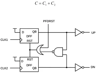
TDC circuit to minimize the area overhead. When a phase difference between CLK0 and CLK1 is detected, the PLL shuts down immediately by disabling PFD1. After that, Loop Filter and VCO function as part of TDC. Fig. 25 shows the modified PFD, which can be disabled using a reset signal.
The TDC structure is modified to simplify the calibration process and enlarge the current capacity. CP2 is designed as a single switch that is controlled using the signal NUP only. Fig. 26—Fig. 28 show the modified circuit and timing behavior. DL1 delays CLK1 to generate the signal, CLK2. CLK2 is always lagging behind CLK0, so UP or NUP contains all of the timing information about CLK0 and CLK1 and signal DN can be neglected.
As shown in Fig. 29, the capacitor of TDC is replaced by Loop Filter. When the loop filter of the tested PLL is used as a capacitor, the charge is pumped into the smaller capacitor C2 first and then redistributed in both capacitors, so the equivalent capacitance is the sum of the capacitances of these two capacitors. The resistor of the loop filter can be neglected since the current flowing through the resistor is zero and the voltage drop across the resistor is zero in the steady state. Loop Filter can be modeled as a capacitor with capacitance C. 2 1 C C C= + (8) DFF DFF RST RST D D QB QB PFDRST UP DN CLK1 CLK2 DFF DFF RST RST D D QB QB PFDRST UP DN CLK1 CLK2
PFD2 CLKA CLKB UP DN CLK1 CLK0 CLK2 DL1 NUP CP2 PFD2 CLKA CLKB UP DN CLK1 CLK0 CLK2 DL1 NUP CP2
Fig. 26 PFD2 circuit design.
CLKA CLKB UP DN CLKA CLKB UP DN CLKA CLKB UP DN CLKA CLKB UP DN
Fig. 27 Timing behavior of PFD2.
CLK0 CLK1 UP DN CLK2 CLK0 CLK1 UP DN CLK2 CLK0 CLK1 UP DN CLK2 CLK0 CLK1 UP DN CLK2
Fig. 28 Timing behavior of circuit with DL1.
PFD VCO CLK1 CLK2 RST C1 CP C2
PFDRST1 PFDRST2 CNTENB CLK0 Vctrl PLL Tracking Phase Detection and Charge Pumping Frequency Variation and Counting PLL Tracking PLL Tracking Phase Detection and Charge Pumping Frequency Variation and Counting PFDRST1 PFDRST2 CNTENB CLK0 Vctrl PLL Tracking Phase Detection and Charge Pumping Frequency Variation and Counting PLL Tracking PLL Tracking Phase Detection and Charge Pumping Frequency Variation and Counting
Fig. 30 Timing diagram of Control Unit.
2.2.2. Control Unit
The BIST process repeats three steps - PLL Tracking, Phase Detection and Counting. Control Unit can be implemented using a finite state machine, as shown in Fig. 30. The PLL Tracking step is the lock-in or pull-in process of the PLL. In step 1, PFD1 is turned on and PFD2 is turned off to allow the PLL to track the phase of the reference clock. In Phase Detection step, PFD1 is turned off and PFD2 is turned on to enable the TDC to detect the phase difference between the reference clock and feedback clock. CP2 pumps some charge to Loop Filter and the voltage of Loop Filter settles down to a particular value. Then, Control Unit proceeds to step 3. In this step, Counter is turned on to count the number of pulses from the DIV output.
The finite state machine uses the negative edge of the reference clock as its clocking signal instead of the positive edge, so PFD1 is turned on for preparation before the positive edges of the reference clock and the feedback clock arrive and it is turned off after the phase detection is completed. The durations of step 1 and step 2 should be longer than the lock-in time of the PLL and the settling time of the loop filter. The duration of step 3 equals Tc in (3).
2.2.3. Calibration
The measurement resolution, kRES, of TDC in (6) must be calibrated. Using the clock
period, T , of VCO as the reference yields an accurate pulse width to calibrate TDC. The o divider is modified to yield a pulse width that equals the clock period of VCO. As shown in Fig. 31, a logic gate and a retiming latch are added to change the duty cycle of the output signal of Divider. After this modification, the pulse width of the Divider output equals the period of the VCO clock.
Fig. 32 shows the calibration circuit of the BIST. The DIV output is connected to CP2 via MUX. In the calibration mode, the control signal MUXSEL changes to a logic high to allow the DIV output signal to pass through MUX. The pulse signal is input to CP2 and changes the voltage of Loop Filter and the frequency of VCO. The pulse width T is the 0 clock period of VCO and the count NCAL of Counter can be obtained. The pulse width is related to the count as
),
( 0
0 k N N
T = RES CAL − (9) where N is the count of Counter if the DIV frequency does not deviate from the original 0 frequency.
The clock period T of VCO varies. It is known as the period jitter. Repeating the 0 calibration process a particular number of times produces a histogram of different NCAL.
D QB D QB D QB D QB Q Q Q Q Q D QB D QB D QB D QB D QB Q Q Q Q Q D QB
The average clock period T0 equals the reference clock period divided by N. The
measurement resolution can be calibrated using the equation,
, 0 0 N N T k CAL RES − = (10)
where NCAL is the average value of NCAL
The purpose of adding DL2 to the calibration circuit is to delay the DIV output signal CLK1 for a clock period of VCO or some longer time to maintain the pulse width of the DIV output after the VCO frequency is changed. Fig. 33 plots the timing diagram of the calibration. The pulse width W1 equals the clock period of VCO before the frequency is changed. W2 is the clock period of VCO after the frequency is changed. DL2 successfully maintains the pulse width of the CLK1 at W1.
0 1 VCO DIV CP1 CLK0 PFDRST1 PFD2 PFDRST2 MUXSEL NUP Counter CNTENB DL1 DL2 CP2 Out CLK2 CLK3 PFD1 CLK1 0 1 VCO DIV CP1 CLK0 PFDRST1 PFD2 PFDRST2 MUXSEL NUP Counter CNTENB DL1 DL2 CP2 Out CLK2 CLK3 PFD1 0 1 VCO DIV CP1 CLK0 PFDRST1 PFD2 PFDRST2 MUXSEL NUP Counter CNTENB DL1 DL2 CP2 Out CLK2 CLK3 PFD1 CLK1
Fig. 32 Calibration circuit.
VCO CLK1 CLK3 Vctrl 1 W W2 VCO CLK1 CLK3 Vctrl VCO CLK1 CLK3 Vctrl 1 W W2
2.3. Experimental Results
Fig. 34 shows the chip photograph. Fig. 35 presents the measurement equipments. The chip is implemented using 0.18μm CMOS technology. The BIST circuit includes the digital part and analog part. The power supplies are separated to prevent the disturbance of the noise from the digital circuit. The Divider output clock signal is measured using an oscilloscope and the BIST output digital signal is measured using a logic analyzer. The noise injected for measurement is produced using a function/arbitrary waveform generator.
As shown in Fig. 36, the noises of various amplitudes and forms are injected into the power line on the PCB through a coupling capacitor to measure the BIST performance in various environments. The power line on PCB can be modeled as an ideal power source in series with a parasitic resistor. The combination of the coupling capacitor and the parasitic resistor constitutes a high-pass filter. A high frequency noise is injected to the tested chip while low-frequency noises are filtered out. The coupling capacitor is designed to be as large as possible to allow more noise to pass through. In this experiment, a 10μF coupling capacitor is used.
The operating frequency of the PLL is 1.25GHz. The reference clock and the feedback clock are operated at 78.125MHz. Fig. 37 shows the PLL feedback clock waveform measured using an oscilloscope and the jitter histogram of 16k hits. 40mV peak-to-peak random noise is injected into the power line. The measured RMS jitter and peak-to-peak jitter are 8.8603ps and 69.3ps, respectively.
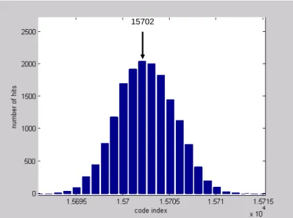
Fig. 38 shows the histogram of the BIST output in the calibration mode in the same environment described above. In the calibration mode, the histogram of the output values of BIST is that of period jitter. According to (10), the average clock period of VCO, which is 800ps when PLL is operated at 1.25GHz, can be used to calibrate the measurement
resolution. The counting time, N , is designed to be 16384 times of the period of the o reference clock. From the histogram of the BIST output, the average value, NCAL , is calculated at 15702. The coefficient, kRES , can be calculated using (10) as 800/(16384-15702)=-1.1730 ps/count. The negative sign of the coefficient means that a negative VCO gain is used.
Fig. 39 shows the histogram of the BIST output in test mode with 40mV peak-to-peak random noise. For comparison, the total number of the data samples measured to produce the histogram equals the number of the hits measured using oscilloscope. Each output value of BIST in test mode represents the phase difference between the reference clock and feedback clock, and the histogram of the BIST output values represents that of timing jitter. Since the measurement resolution, kRES, in (6) was calibrated, the jitter magnitude can be determined by simply multiplying the output values of the BIST output data by the measurement resolution. The peak-to-peak jitter and RMS jitter of the PLL in this case are 1.1737*(15877-15940)=73.899ps and 1.1737*8.937=10.4893ps, respectively.
Fig. 40, Fig. 41, and Fig. 42 show the histograms measured using the oscilloscope, BIST in calibration mode and BIST in test mode, respectively, when the power line is injected with 40mV, 10MHz sinusoidal noise. The RMS jitter and peak-to-peak jitter measured using the oscilloscope are 18.6970ps and 80.4ps, respectively. The RMS jitter and peak-to-peak jitter measured using the BIST are 22.8011ps and 95.8357ps, respectively. Since the noise is sinusoidal, the histograms of period jitter and timing jitter have bowl shapes, as expected.
Table 1 presents more cases. Fig. 43 and Fig. 44 compare the RMS jitter and peak-to-peak jitter measured using the oscilloscope and BIST circuit. The measurement errors in most of the cases are under 20%, except in the case with 1MHz noise. As
mentioned, the TDC utilizes VCO and Loop Filter of the tested PLL as part of the circuit, but the initial value of the VCO control voltage is not constant due to supply noise and PLL tracking ability. This is believed to be the main cause of the measurement error in the experimental results. Table 2 and Table 3 summarize this work. The area overhead is 36.7%. The supply voltage is set to 1.85V because the BIST circuit does not function well when the voltage is under 1.85V. The problem has not been solved. However, the problem may probably arise in the analog circuit of BIST because the digital circuit is insensitive to a power supply voltage.
The measurement time, 3.44s, is too long for test application. To improve the performance, a high speed counter such as a ripple counter could be connected directly to the VCO for frequency measurement. It could shorten the measurement time to be about one tenth or less. The Multi-Phase Phase Detector [61] could also be applied to further shorten the measurement time to be less than one-hundredth of this work.
Table 4 compares the results herein with previous works. This work has a resolution of 1.17ps, which is the finest of all, except the one (1ps) using an accurate analog bias to fine tune the delay line [8]. The measurement error is relatively small (14.6%), but dependent on the noise frequency, so modifying the circuit to have a constant initial VCO control voltage is required. The test time is much longer than the other approaches because this work achieves good resolution at the expense of measurement time.
PLL
BIST digital
BIST analogPLL
BIST digital
BIST analogFig. 34 Chip photograph.
Power line Coupling capacitor Noise Chip Power supply Parasitic resistor Power line Coupling capacitor Noise Chip Power supply Parasitic resistor
Fig. 36 Injecting noise into the power line.
Fig. 37 PLL DIV output clock jitter with 40mV p-p random noise.
15702 15702
15940
15877 15940
15877
Fig. 39 Histogram of BIST output in test mode with 40mV p-p random noise.
15699 15699
Fig. 41 Histogram of BIST output in calibration mode (40mVp-p 10MHz sinusoidal).
15951
15869 15951
15869
Fig. 43 RMS jitter measured using oscilloscope and the BIST circuit.
Table 1 Jitter measured using oscilloscope and the BIST circuit. Type Amp. p-p (mV) Fr (MHz) Osc RMS (ps) Osc p-p (ps) BIST RMS (ps) BIST p-p (ps) RMS error (%) p-p error (%) Random 0 - 5.4502 44.9 6.2464 47.6284 14.60864 6.076615 Random 20 - 6.3349 47.6 7.4476 59.9492 17.5646 25.9437 Random 40 - 8.8603 69.3 10.4831 73.899 18.38538 6.701299 Random 60 - 12.1454 94.2 14.1385 99.682 16.41033 5.819533 Random 80 - 15.724 119.6 17.9926 121.9933 14.42763 2.001087 Random 100 - 19.1059 139.1 21.9112 152.5462 14.6829 9.666571 Random 120 - 22.588 160 25.5602 174.5728 13.15831 9.108 Random 140 - 26.4569 183.3 29.687 195.7189 12.20891 6.775177 Random 160 - 30.0448 216.7 33.597 221.509 11.82301 2.219197 Sin 40 50 10.9452 60 13.2048 72.5872 20.64467 20.97867 Sin 80 50 20.089 87.1 24.0374 104.1341 19.65454 19.55695 Sin 40 10 18.697 80.4 22.8011 95.8357 21.95058 19.19863 Sin 80 10 36.8383 133.3 43.8717 161.5182 19.09263 21.16894 Sin 80 1 5.2596 41.8 7.6686 54.8198 45.80196 31.14785 Sin 160 1 7.0429 46.7 10.9957 66.5088 56.12461 42.41713
Table 2 PLL specifications.
CMOS technology 0.18µm CMOS
VDD 1.85V Power consumption (PLL+BIST analog part) 40mW
Area 300X300µm2
Reference clocks 78.125MHz VCO frequency 1.25GHz
RMS jitter 5.4502ps Peak-to-peak jitter 44.9ps
Table 3 BIST specifications.
VDD 1.85V
Power consumption (Digital part) 0.22mW Area (BIST analog) 190X35µm2 (7.4%) Area (BIST digital) 310X85µm2(29.3%)
Resolution 1.17ps
Error 14.6% Reference clocks 78.125MHz
Table 4 Performance Comparison. Type Res. Scope
(RMS jitter)
BIST (RMS jitter)
Error Meas. time (one-shot) Tech. Sunter, ITC, 1999 [1] Delay line 40ps 88.8ps 72ps 18.9% 4.16ns 0.6µm CMOS Jenkins, CICC, 2007 [8] Delay line 1ps 5.7ps 5.5ps 3.5% 1.85ns 90nm CMOS Aloisio, NSSCR, 2009 [10]
Delay line 11.3ps - - - 12.6ns FPGA
Abaskharoun, CICC, 2001 [16] Vernier 18ps 30.4ps 27.6ps 9.2% 40ns 0.35µm CMOS Levine, CDT, 2005 [27] Sampling Offset 9.8ps 13.5ps 14.5ps 7.4% 40ns 0.18µm CMOS Chan, CICC, 2001 [22] Vernier Ring 67ps 22ps 66ps 200% 154ns 0.18µm CMOS Xia, ISVLSI, 2005 [25] Vernier Ring 18.5ps 42.7ps 62.7ps 46.8% - 0.18µm CMOS Chen, CICC, 1999, [30] Pulse-shrink ing Ring 68ps - - - 10µs 0.35µm CMOS Henzler, ISSCC, 2008 [33] Local Passive 4.7ps - - - 5.56ns 90nm CMOS Chen, ESSCIRC, 2006 [39] Time Amplifier 50ps - - - 6.67us 0.35µm CMOS Taylor, ITC, 2004 [43] TVC with flash ADC 55ps 52ps 80ps 53.8% 10ns 0.25µm BICMO S Ishida, ISSCC, 2005 [47] Hybrid - 95.7ps 83.5ps 12.7% - 0.18µm CMOS Sunter, DTC, 2004, [50] Under-samp ling 1.4ps 43ps 50ps 16.3% 103.7ns FPGA This work TVC with
VCO
1.17ps 5.45ps 6.25ps 14.6% 210µs 0.18µm CMOS
Chapter 3
BIST for Spread-Spectrum Clocks
3.1. BIST Methodology Overview
Fig. 45 shows an SSC generator (SSCG) and the proposed BIST methodology. A triangular waveform is generated according to the modulation profile of a 5000ppm down-spreading and a 30kHz modulation frequency. The Sigma-Delta Modulator (SDM) is used to control the 10-phase 5-stage Voltage-Controlled Oscillator (VCO) such that it oscillates in accordance with the modulation profile.
The BIST module is composed of hardware and software. The hardware comprises a 10-phase Multi-Phase Phase Detector (MPD), as shown in Fig. 46. The MPD uses ten D Flip-Flops (DFFs) to compare the reference clock with the ten clock phases generated by the VCO. The reference clock is used as a triggering signal of the DFFs, and the ten clock phases are the signal being sampled. When the clock edge of the reference clock comes,
PFD LF VCO MUX 1/N Ctrl Multi-Phase Clock MPD HPF DSP Jitter LPF Modulation profile DSP SSCG BIST ΣΔ REF PFD LF VCO MUX 1/N Ctrl Multi-Phase Clock MPD HPF DSP Jitter LPF Modulation profile DSP SSCG BIST ΣΔ REF
the ten clock phases are sampled and the DFFs output 10-bit thermal meter code. The transition bit of the thermal meter code represents the detected phase. The phase-shift detector detects the phase shift by comparing the detected phases at the first triggering time and the next triggering time.
An example is shown in Fig. 47. Phase 5 is sampled by the first reference clock edge, and Phase 7 is sampled by the next reference clock edge. A phase shift of 0.2UI is detected. Notably, if the frequency deviation of the SSC is too large, the phase shift may exceed 1 UI. If so, a faster reference clock is needed. When frequency deviation is 6MHz (5000ppm) and a reference clock period of 50ns, phase shift is 0.3UI, which is smaller than 1UI. The next step in phase detection process is to accumulate each phase shift to recover the absolute phase. Notably, without jitter, the accumulated phase is the integration of the modulation profile (Fig. 17(a)). Because modulation profile is the timing diagram of the SSC frequency, the integration of frequency in time is the absolute phase.
If the SSCG doesn’t have multi-phase clocks, the single phase clock must be operating at higher speed. This clock can be input to a high speed single-phase phase detector, such as a DFF, and the detected serial data is processed by a de-serializer to have the output similar with that of the MPD. Another approach is converting a single-phase clock to a multi-phase clock by a ring type shift registers.
Multi-phase SSC P h as e S h if t De tec to r Ac c u m u la to r SSC Phase Encode r Reference Clock 1 φ 2 φ 3 φ 10 φ Multi-phase SSC P h as e S h if t De tec to r Ac c u m u la to r SSC Phase Encode r Reference Clock 1 φ 2 φ 3 φ 10 φ
The software in the BIST modules comprises a digital signal processing (DSP) program that utilizes the on-chip DSP or microprocessor to extract jitter and the modulation profile after obtaining the accumulated phase using the MPD. Conceptually, the modulation profile can have a frequency as low as 30kHz. Therefore, a Low-Pass Filter (LPF) can extract the modulation profile from the accumulated phase. The high-frequency components of jitter are defined by the SATA standard. Therefore, jitter can be obtained using a High-Pass Filter (HPF). Notably, additional DSP functions are required to acquire the modulation profile and jitter after filtering. Fig. 48 shows the jitter measurement model, where
φ
SSC is the ideal accumulated phase. Two added noise sources are jitter (φ
J) andMPD phase quantization noise (φE). The methodology has two processing paths—the HPF path for jitter measurement and LPF path for modulation profile extraction.
For jitter measurement, the accumulated phase passes through the HPF. After that, only high-frequency components (
φ
JH+EH) remain, where JH is high-frequency jitter andEH is high-frequency quantization noise. The power spectral density (PSD) function of high-frequency components, SφJH+EH, can be obtained by taking the square of the Fast Fourier Transform (FFT). UI 2 . 0 5 7−φ = φ UI 5 . 0 0.7UI UI 3 . 0 7 10−φ = φ UI 0 . 1 Reference Clock Phase Shift Accumulation 7 φ 6 φ 5 φ 4 φ 3 φ φ6φ7φ8 φ9 φ9 φ10φ1 φ2φ3 SSCG Clock
)). ( ( ) (f FFT2 t SJH EH = JH+EH +
φ
φ (11)The jitter variance, or jitter power, is the integration of S JH EH +
φ in the frequency domain.
, ) ( 2 / 2 / 2 ,
∫
− + = + ref ref EH JH f f RMS EH JH Sφ f dfφ
(12)where f is the reference clock frequency and RMS is root mean square value. Because ref
ref
f is the sampling rate of MPD, so the frequency band of the signals within DSP circuit does not exceed the range of half of f , based on DSP theories. ref
Since jitter and quantization noise are independent random variables, jitter variance can be obtained by . 2 , 2 , 2 ,RMS JH EHRMS EHRMS JH
φ
φ
φ
= + − (13)Since quantization noise is typically regarded as white noise, its PSD is . 12 2 ref MPD f S E ⋅ Δ = φ (14)
Since the transfer function of the HPF is known, φEH,RMS is obtained as
. ) 2 ( 2 / 2 / 2 2 ,
∫
− ⋅ = ref ref E f f HPF RMS EH H jπ
f Sφ dfφ
(15)The modulation profile is extracted using the LPF. After the accumulated phase passes
SSC φ J φ φE EH JH+ φ EL JL SSC+ + φ Modulation Profile HPF DSP LPF DSP HPF DSP LPF DSP Jitter PSD,RMS, and Histogram
through the LPF, only the low-frequency component
φ
SSC+JL+EL remains, where JL islow-frequency jitter and EL is low-frequency quantization noise.
φ
SSC+JL+EL approximates SSCφ
, because low-frequency jitter is relatively small. Most of the low-frequency jitter of the VCO is filtered out by the PLL, as PLL acts like a high pass filter for VCO noise. Most high-frequency components of quantization noise are filtered out by the LPF. As mentioned, the accumulated phase shift is the integration of the modulation profile in time. Now, by taking the reverse operation, the derivative ofφ
SSC+JL+EL generates the modulation profile.. ) ( ) ( dt t d t f =
φ
SSC+JL+EL (16)Via (11)~(16), the jitter and modulation profile can be extracted from the accumulated phase obtained by the MPD.
The next step is to validate the extracted result. Without dedicated SSC timing jitter measurement instruments, verifying that such a methodology can effectively measure SSC jitter is difficult. In next section, the work derives an equation that correlates timing jitter in SSC mode and non-SSC mode of the same PLL. In non-SSC mode, jitter can be measured by external instruments. SSC jitter is estimated using measured results from the non-SSC mode and the derived equation. Thus, this work can cross check and validate both the BIST methodology and the jitter estimation method.
3.2. SSC Jitter Estimation
In this section, a jitter estimation method that correlates a non-SSC clock timing jitter and the corresponding SSC jitter is used to validate the BIST methodology. An equation for SDM noise calculation is also presented for the specific SSCG in this work.
The SSCG is made by a fractional-N PLL with a triangular modulation profile. Some prior arts have developed the jitter estimation methods for fractional-N PLLs [62][63]. In
these studies, a PLL is modeled as an ideal filter and a common SDM is used. However, a PLL transfer function has a peak, which increases jitter magnitude. Additionally, the SDM used in this work is specially designed so a common analysis is not applicable. More accurate model and a dedicated analysis are presented as follows.
Fig. 49 shows the noise model of a SSCG circuit with a third-order loop filter. Based on spectral analysis, the output jitter PSD of the SSCG and noise sources are related as follows: , 2 2 2 2 (f) S f) (j H (f) S f) (j H (f) S (f) S (f) S VCO ΣΔ PLLVCO PLL PLL Φ VCO Φ ΣΔ Φ Φ Φ ⋅ + ⋅ = + = ΣΔ π π (17) where PLL Φ
S is the PSD of the PLL output jitter.
PLL Φ S is composed of S (f) PLL Φ ΣΔ and ) (
SΦPLLVCO f , the PSD of the PLL output jitter caused by the noise from the SDM and VCO. Additionally,
ΣΔ
Φ
S and SΦVCO are the PSDs of the SDM and VCO noise, respectively, and
ΣΔ
H and HVCO are the transfer functions from noise sources, φΣΔ and φVCO, to the PLL output, respectively. With this information,
PLL
Φ
S can be derived by (17). The RMS jitter is calculated as . 2 ,RMS SΦPLL(f )df J