國立交通大學
電子工程學系 電子研究所碩士班
碩士論文
鎳鍺化物與 N 型鍺接面摻雜析離對於
蕭基位障的影響:透過第一原理計算
Schottky Barrier Height of the NiGe/n-type Ge Contact
with Dopant Segregation: A First-principles Study
研究生 : 林翰奇
指導教授 : 崔秉鉞 教授
共同指導教授 : 林炯源 教授
鎳鍺化物與 N 型鍺接面摻雜析離對於蕭基位障的影響:
透過第一原理計算
Schottky Barrier Height of the NiGe/n-type Ge Contact
with Dopant Segregation: A First-principles Study
研究生 : 林翰奇 Student : Han-Chi Lin 指導教授 :崔秉鉞 Advisor : Bing-Yue Tsui 共同指導教授 : 林炯源 Co-advisor : Chiung-Yuan Lin
國立交通大學 電子工程學系 電子研究所
碩士論文 A Thesis
Submitted to Department of Electronics Engineering and Institute of Electronics College of Electrical Engineering and Computer Engineering
National Chiao Tung University in Partial Fulfillment of the Requirement
for the Degree of Master of Science in
Electronic Engineering 2013
Hsinchu, Taiwan, Republic of China 中華民國一0二年九月
I
鎳鍺化物與 N 型鍺接面摻雜析離對於蕭基位障的影
響: 使用第一原理計算
研究生 : 林翰奇 指導教授 : 崔秉鉞
共同指導教授 : 林炯源
國立交通大學電子工程學系 電子研究所碩士班
摘要
近年來隨著傳統的矽金氧半場效電晶體技術已經逐漸到達其微縮的極
限。為了能夠持續追求元件性能的提升,鍺因為它的載子擁有優越的本質
遷移率,被認為在不久的將來可以取代矽作為通道的材料而受到廣泛的研
究。然而一般的N型摻雜物例如磷與砷在鍺基板不止固態溶解度比在矽基
板還低而且具有更快的擴散速率,所以很難製作出深度很淺的接面。更糟
的是,接面的費米能階被釘扎在很靠近鍺價帶的頂端,造成相當高的電子
蕭基位障。實驗上發現透過摻雜析離技術可以使得摻雜物在界面析離進而
達到更淺的接面深度與更濃的摻雜濃度。但是,摻雜物對於改變界面特性
所扮演的角色仍然不是很清楚。
在本篇論文中,我們只用單一的鎳鍺化物(112)晶相去簡化真實
的多晶鎳鍺化物並與鍺形成接面結構,然後透過第一原理計算使用 LDA 交
II
換相關能泛函研究N型摻雜物在界面的行為以及使用 HSE06 泛函探討摻雜
物析離在界面是否可以有效降低鎳鍺化物與鍺接面的物理蕭基位障。
對於一般的N型摻雜物例如磷與砷而言,我們的計算結果顯示這兩種
摻雜物都會在界面析離,雖然磷較偏好析離在界面靠近鎳鍺化物的那一側
而砷則是偏好在鍺那一端。這些結果建議我們假若要摻雜磷,在形成鎳鍺
化物先植入磷會是個較好的製程選擇;對於摻雜砷,不管製程是在形成鎳
鍺化物之前或是之後植入砷,砷都會移到鍺那一端並且堆積在界面。
然後,我們指出這兩種摻雜物析離在界面靠近鍺那一端造成鎳鍺化物
與鍺接面的物理蕭基位障降低的量少於 0.1eV,而這麼小的降幅是因為很強
的費米能階釘扎效應所造成。順帶一提,當摻雜磷在界面靠近鎳鍺化物的
那一側不具有任何降低物理蕭基位障的效果。總結以上的結果,我們認為
摻雜析離造成鎳鍺化物與鍺接面特性的改善主要歸功於增加在界面附近的
摻雜濃度,少部分是由於物理蕭基位障降低的貢獻。
最後我們探討當摻雜氮這種特殊的情況,計算的結果指出氮可以析離
在界面,然而也產生大量的界面態散佈在整個鍺的能隙。雖然鍺的等效導
帶邊界透過連續分布的界面態延伸而更接近費米能階,然而界面態在遠離
界面約 17 埃即消失殆盡,所以鎳鍺化物與鍺接面的物理蕭基位障還是幾乎
III
沒有任何改變。
以上這些第一原理的計算結果給予我們更深入的了解對於摻雜物在鎳
鍺化物與鍺接面所扮演的角色,也與實驗所觀察到的結果相互呼應。將來,
更進一步的計算希望可以協助新製程的開發。
IV
Schottky Barrier Height of the NiGe/n-type Ge Contact
with Dopant Segregation: A First-principles Study
Student: Han-Chi Lin Advisor: Bing-Yue Tsui
Co-advisor: Chiung-Yuan Lin
Department of Electronics Engineering
Institute of Electronics
National Chiao Tung University
Abstract
Recently, traditional Si-based MOSFETs are approaching its fundamental scaling limits, and then Ge has been comprehensively explored as a potential channel material to replace Si due to its high intrinsic carrier mobility for further performance enhancement. Nevertheless, the shallow junction depth is hard to form since the conventional n-type dopants such as phosphorous and arsenic have not only lower solid solubility but also faster diffusion rate in Ge substrate than in Si. Moreover, strong Fermi-level pinning near the valence band edge of Ge leads to high electron Schottky barrier height. Dopant segregation technique has been proposed to achieve shallower junction depth and heavier dopant concentration experimentally due to dopant segregated around the interface. However, the role of dopants at the NiGe/Ge interface is not clear.
In this thesis, we build the realistic polycrystalline phases NiGe/Ge contact by including NiGe (112) phase only, and then the first-principles calculations are employed to investigate
V
the behaviors of the n-type dopant around the interface by LDA functional and whether the physical Schottky barrier height of the NiGe/Ge contact is reduced by dopant segregation or not is calculated by HSE06 hybrid functional.
For the conventional n-type dopant such as phosphorous and arsenic, our calculations show that those two elements may be segregated at the interface, but the preferred segregated site of phosphorous and arsenic are on the NiGe and Ge side, respectively. These results suggest that phosphorous would be a better choice for implantation before germanide process, while arsenic can migrate into the Ge layer and pile up at the interface in both implantation before and after germanide processes.
Then, we show that the physical Schottky barrier height of the NiGe/Ge contact modified by dopant segregation using those two elements on the Ge side is reduced by less than 0.1 eV. This small value is due to the strong Fermi-level pinning effect. By the way, there is no effect to modify the physical Schottky barrier height by doping phosphorous on the NiGe side. To sum up, the improvement of the NiGe/n-type Ge junction characteristics by dopant segregation using phosphorous and arsenic are mainly attributed to the increase of dopant concentration around the interface and partially attributed to the reduction of the physical Schottky barrier height.
For the specific case using nitrogen dopant, the calculated results show that it can be segregated around the interface but yield a large number interface states spreading the Ge bandgap. Although the effective conduction band edge is closer to the Femi level due to continuous interface states, the physical Schottky barrier is almost unchanged since the interface states disappear at about 17 Å away from the interface.
VI
NiGe/Ge interface and can explain the experimental observations very well. Further calculations can also help new process development.
VII
致謝
在攻讀研究所碩士班的這兩年生涯中,首先要感謝指導老師 崔秉鉞博士給予我開 啟第一原理計算的鎖匙以及研究的目標,讓我可以用自己感興趣的方法研究我們覺得有 意義的主題。對於自己較不熟悉的製程與材料分析上的問題,老師都很有耐心得一一解 答我內心的疑問,答案往往也是一針見血。接下來感謝共同指導老師 林炯源博士,從 一開始從無到有地教導我理論計算的基礎到中後期當我在研究上遇到計算上的瓶頸時, 往往在一天內就可以與老師討論,並且得到很有用且具有彈性的建議順利解決問題。 對於實驗室的大家,首先要感謝已經畢業的振銘學長與子瑜,你們是我進入碩班學 習的榜樣,而且不管是專業上還是生活上的困惑都可以與你們討論。謝謝元宏學長、罩 哥與嶸健學長,不管問什麼專業上的問題好像都難不倒你們一樣,尤其是有幾次問元宏 學長比較微觀的問題,當學長對於自己的答案不是很確定時,都會很有耐心得找書或是 查資料,最後告訴我一個正確的答案。而對於一起共患難的滷蛋以及喇叭,能在碩班認 識你們,真的沒有什麼遺憾了,謝謝你們,喇叭接下來也要好好加油優!謝謝璽允、泰 勞、國丞、雪君有你們陪我談天說地遇到挫折相互鼓勵,也謝謝昕翰、立偉與小弘。 謝謝威智與庭煦學長教我跑第一原理計算的程式,並且根據他們之前的經驗給予我 相當適當的建議,幫我減少很多沒有必要的錯誤,尤其謝謝庭煦學長,在我需要跑一些 比較久的計算的時候,你總是為我空下 17 的計算資源讓我使用,真的很感謝你。也謝 謝昆霖與聖瀚很迅速地幫忙處理工作站的問題,讓我可以無後顧之憂地跑程式! 最後感謝在我背後一直支持我讀完碩班的家人,謝謝爺爺 林智惠先生與阿嬤 林沈 素琴 女士,你們省吃儉用就只是為了讓我可以好好專心讀書,真的很謝謝你們的栽培。 也謝謝哥哥在我無法陪伴在爺爺奶奶身邊時,照顧他們而且幫我解釋一些他們擔心的事 情,讓他們不會這麼擔心,謝謝你!VIII
Contents
Abstract (Chinese) ... I Abstract (English) ... IV Acknowledgements ... VII Contents ... VIII List of Tables ... XI List of Figures ... XIIChapter 1 Introduction ... 1
1.1 Si-based MOSFETs Scaling Challenges of Source/Drain Design... 1
1.1.1 Overview ... 1
1.1.2 The Impact of the Total On-resistance on MOSFETs Scaling ... 2
1.2 Properties of Metal/Semiconductor Contacts ... 3
1.2.1 Schottky Barrier Height ... 3
1.2.2 Fermi-level Pinning ... 3
1.2.3 Specific Contact Resistance ... 4
1.3 Modified Schottky Barrier (MSB) Height Method ... 5
1.4 Pros and Cons of Germanium ... 6
IX
1.6 Organization ... 10
Chapter 2 Calculation Methods ... 16
2.1 Representational Approaches before Density Functional Theory ... 16
2.1.1 The Born-Oppenheimer approximation... 17
2.1.2 The Hartree-Fock approximation ... 18
2.2 Density Functional Theory (DFT) ... 21
2.2.1 The Hohenberg-Kohn Theorem ... 22
2.2.2 The Kohn-Sham Formulation ... 24
2.3 The Exchange-correlation functional ... 27
2.3.1 The local density approximation (LDA) ... 27
2.3.2 The generalized gradient approximation (GGA) ... 29
2.3.3 Hybrid functionals ... 31
Chapter 3 Results and Discussion ... 34
3.1 Choosing Exchange-correlation Functional ... 34
3.2 Structural Modeling of the NiGe/Ge Contact ... 35
3.2.1 Behaviors of Segregated Dopant around the Interface ... 37
3.2.2 Barrier Height Modified by Dopant Segregation ... 38
X
Chapter 4 Conclusion and Future works ... 61
4.1 Conclusions ... 61
4.2 Future Works ... 63
References... 64
XI
List of Tables
Chapter 1
Table 1-1 Material characteristics of alternative channel materials [10]. ... 11
Chapter 3
Table 3-1 Calculated lattice constant (second row) and also the Ge-bulk bandgap (fourth to eighth rows) at the various lattice constant using different exchange-correlation functionals. The experimental lattice constant and bandgap are 5.658 Å and 0.785 eV [42], respectively. ... 43 Table 3-2 Specific lateral surface vectors chosen for the NiGe(112)/Ge(001) interface strucutre. ... 44 Table 3-3 Specific lateral surface vectors chosen for the NiGe(210)/Ge(001) interface strucutre. ... 44 Table 3-4 Specific lateral surface vectors chosen for the NiGe(111)/Ge(001) interface strucutre. ... 45 Table 3-5 Total energy of the various choices of lateral matching with NiGe(112)T4 and Ge(001) slabs. ... 45 Table 3-6 Total energy of the various choices of lateral matching with NiGe(112)T8 and Ge(001) slabs. ... 46
XII
List of Figures
Chapter 1
Figure 1-1 Number of transistors on the CPU has been increased from 1971 to 2011; the line corresponds to exponential growth with Moore’s law. (source: Wikipedia) ... 12 Figure 1-2 N-type Metal-Oxide-Semiconductor Field-Effect-Transistor (nMOSFET) device simulation showing series and strained Si channel resistances becoming equivalent at approximately the 32 nm logic node [2]. ... 12 Figure 1-3 Schematic representation of source/drain structure and series resistance components [3]. ... 13 Figure 1-4 Relative contribution from each component of the resistance to series resistance for different technology nodes [4]. ... 13 Figure 1-5 Schematic band diagram of band bending according to the Schottky-Mott model of the metal/n-type semiconductor: (a) Before contact and (b) after contact formation [26]. ... 14 Figure 1-6 Schematic band diagram of band bending according to the Bardeen model of the metal/n-type semiconductor: (a) Before contact and (b) after contact formation. The Fermi-level is pinned by the high density of surface states at the semiconductor interface [26]. ... 14 Figure 1-7 Conduction mechanics for metal/semiconductor contacts, (a) thermionic emission (b) thermionic-field emission (c) field emission. ... 15 Figure 1-8 Sub-100 nm transistor technology scaling. (source: Intel Corp.) ... 15
XIII
Chapter 3
Figure 3-1 Conventional cell of the Ge bulk. ... 47 Figure 3-2 Atomic structure of the NiGe bulk. ... 47 Figure 3-3 Calculated band structure of the Ge bulk by HSE06. The red crosses stand for the high-symmetry points as measured by thr photoemission experiments. The enerygy reference is set at the Fermi-level. ... 48 Figure 3-4 Process flow of the self-aligned NiGe n+/p junction. ... 48 Figure 3-5 X-ray diffraction (XRD) sprectrum of the NiGe/Ge structure formed by 350˚C annealing shows polycrystalline NiGe phases. ... 49 Figure 3-6 Lateral cell shape of the NiGe(112), (210), and (111) slabs on the Ge(001) surface. ... 49 Figure 3-7 One of the surface terminations of the NiGe(112) slab, called NiGe(112)T4 slab, contains 4 atoms (2 Ni and 2 Ge atoms) per lateral unit cell. ... 50 Figure 3-8 One of the surface terminations of the NiGe(112) slab, called NiGe(112)T8 slab, contains 8 atoms (4 Ni and 4 Ge atoms) per lateral unit cell. ... 50 Figure 3-9 Various choices of lateral matching of the NiGe(112) and Ge(001) slab. The a and b stand for the origin offset of the NiGe slab at x and y direction, respectively. ... 51 Figure 3-10 Atomic structure of the NiGe/Ge contact. ... 51 Figure 3-11 Total energy of the NiGe/Ge interface structure with one Ge atom being substituted for a phosphorous, where the energy reference is taken to be the
XIV
cases with the most left substitutional sites. ... 52 Figure 3-12 Total energy of the NiGe/Ge interface structure with one Ge atom being substituted for an arsenic, where the energy reference is taken to be the cases with the most left substitutional sites. ... 52 Figure 3-13 Secondary ion mass spetroscopic (SIMS) profiles shows the phosphorous segregation at the NiGe/Ge(001) interface with a NiGe thickness of 60 nm [23]. ... 53 Figure 3-14 Secondary ion mass spetroscopic (SIMS) profiles shows the arsenic segregation at the NiGe/Ge(001) interface with a NiGe thickness of 60 nm [23]. ... 53 Figure 3-15 Bandgap of the Ge(001) slab as a function of the nuber of atomic layers. ... 54 Figure 3-16 Partial density of states (PDOS) of the Ge atom in the pure 16-layers Ge(001) slab. ... 54 Figure 3-17 Partial density of states (PDOS) of the Ge atom labeled as SG9b (see Figure 3-10) in the undoped NiGe/Ge interfacial structure. ... 55 Figure 3-18 Partial density of states (PDOS) of the Ge atom labeled as SG9b (see Figure 3-10) in the NiGe/Ge interface structure when doping phosphorous at the most stable position... 55 Figure 3-19 Partial density of states (PDOS) of the Ge atom labeled as SG9b (see Figure 3-10) in the NiGe/Ge interface structure when doping phosphorous at the metastable site. ... 56 Figure 3-20 Partial density of states (PDOS) of the Ge atom labeled as SG9b (see Figure
XV
3-10) in the NiGe/Ge interface structure when doping arsenic at the most stable position. ... 56 Figure 3-21 Current-voltage characteristics of the NiGe/Ge junction without and with phosphorous segregation [44]. ... 57 Figure 3-22 Current-voltage characteristics of the NiGe/Ge junction without and with arsenic segregation [44]. ... 57 Figure 3-23 Partial density of states (PDOS) of the Ge atom labeled as SG9b (see Figure 3-10) in the NiGe/Ge interface structure when doping nitrogen at the most stable position. ... 58 Figure 3-24 Partial density of states (PDOS) of the Ge atom labeled as SG1b (see Figure 3-10) in the NiGe/Ge interface structure when doping nitrogen at the most stable position. ... 58 Figure 3-25 Partial density of states (PDOS) of the Ge atom labeled as SG5b (see Figure 3-10) in the NiGe/Ge interface structure when doping nitrogen at the most stable position. ... 59 Figure 3-26 Partial density of states (PDOS) of the Ge atom labeled as SG13b (see Figure 3-10) in the NiGe/Ge interface structure when doping nitrogen at the most stable position. ... 59 Figure 3-27 Bandgap of the Ge atom in the NiGe/Ge interface structure when doping nitrogen at the most stable position as a function of the distance far from the interface. The gray lines stand for the interface states spreading the Ge bandgap. ... 60
1
Chapter 1
Introduction
1.1 Si-based MOSFETs Scaling Challenges of Source/Drain Design
1.1.1 Overview
The integrated circuits (ICs) industry has been growing rapidly, benefiting from the dimension scaling of Si-based metal-oxide-semiconductor field-effect-transistors (MOSFETs) for more than half a century. Since then, more and more transistors are able to be integrated into a single chip as shown in Figure 1-1. Moore’s law is named after Gordon E. Moore who projected firstly the number of transistors on ICs doubles approximately every two years in 1965 [1]. The scaling not only decreases production cost per transistor and power consumption but also increases the circuit density and device speed.
A successful device design tends to enhance the on-current at the allowable off-state leakage for the performance requirements during scaling. However, several negative short-channel effects would arise from device scale-down. As the gate length of MOSFETs are reduced, the channel potential influenced by the source/drain increases relative to the gate. Escalating off-state leakage arises from threshold voltage roll-off and drain-induced barrier lowering (DIBL), which describe smaller threshold voltage at shorter gate length and higher drain voltage, may hinder transistor scaling because of significant passive power consumption. In order to reduce the source and drain influence on the channel potential in bulk device, the ultra-shallow junction formation technologies are necessary to minimize these short-channel effects.
2
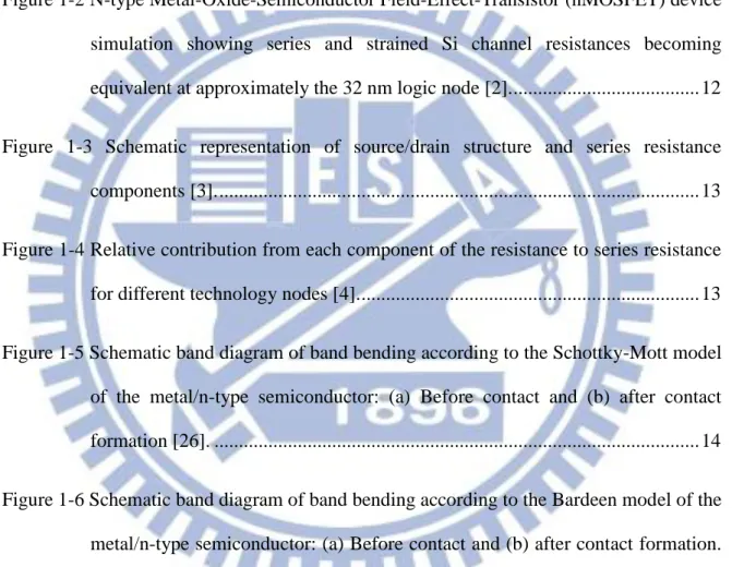
1.1.2 The Impact of the Total On-resistance on MOSFETs Scaling
The total on-resistance of the MOSFETs is the summation of channel resistance and series resistance. The channel resistance diminishes aggressively with the scaling of the gate length and the carrier mobility enhancement by uniaxial stain technology, while the series resistance is difficult to be reduced due to the decrease of contact area and junction depth. Unfortunately, escalating series resistance might limit the device on-current for performance enhancement. Figure 1-2 shows the simulated channel resistance and series resistance of NMOSFET at various technology nodes. It demonstrates the increasing trend of series resistance, converse to the trend of decreasing channel resistance with transistor scaling. It is observed that the series resistance would be comparable to the channel resistance at the 32-nm logic node [2]. Therefore, reduction of series resistance represents one of the fateful challenges for continued aggressive scaling.
The series resistance can be divided into four components: source/drain extension (SDE) to gate overlap resistance (Rov); SDE resistance (Rext); deep source/drain resistance (Rdp); and
silicide-diffusion contact resistance (Rcsd) as shown in Figure 1-3 [3]. To successfully optimize
the source/drain design for lower series resistance, it is important to understand the relative contribution of each component. Among these components, the Rcsd and Rov are the dominant
components and account for more than 80% of the total series resistance at all technology nodes as shown in Figure 1-4 [4]. It is noted that the contribution of Rcsd escalates as the transistor
scaling, while Rov is almost at the same level. As a result, the Rcsd is the most serious component
3
1.2 Properties of Metal/Semiconductor Contacts
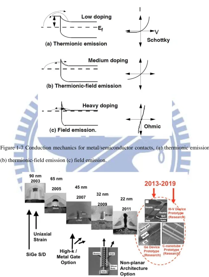
1.2.1 Schottky Barrier Height
For reduction of contact resistance, the characterizations of metal/semiconductor should be prior to understanding. The rectifying properties of the metal/semiconductor contacts discovered by Ferdinand Braun in 1874 are determined by the barrier height of the majority carrier using the simple model proposed independently by Schottky and Mott [5]. The barrier height equals the energy difference between the Fermi level and the edge of the respective majority carrier band, i.e., the conduction-band minimum for n-type semiconductors or the valence-band maximum for p-type semiconductors [6].
In the case that an n-type semiconductor and a metal with higher work function come in electric contact, the two Fermi levels are forced to coincide and electrons pass from the semiconductor into metal. The excess of negative charge on the metal surface and the positive space-charge in the depletion layer near the semiconductor surface form an interface dipole and result in band bending regime as shown in Figure 1-5. The n-type Schottky barrier height (SBH) calculated by the Schottky-Mott model is given by:
,
where is the barrier height, is the metal work function, and is the electron affinity, which describes the energy difference between the bottom of the conduction band and the vacuum level at the semiconductor surface.
1.2.2 Fermi-level Pinning
The above equation shows that the barrier height depends linearly on the metal work function and demonstrates by the experimental results of ionically bonded semiconductors [6].
4
However, some covalently bonded semiconductors such as Si, Ge, and GaAs do not confirm this relationship because the barrier height depends weakly on the metal work function. In 1947, Bardeen proposed the different model to explain the insensitivity of the Schottky barrier height to the metal work function as shown in Figure 1-6 [7]. It is shown that if the high density of localized interface states at the semiconductor interface distribute in the semiconductor energy bandgap, those interface states would absorb most of the majority carriers on the semiconductor side. Consequently, different excess charge density on the metal side will cause only slight variations of the space-charge density. As a result, the barrier height will become almost independent of the metal work function. Such behavior is called Fermi-level pinning (FLP).
1.2.3 Specific Contact Resistance
In order to simply compare values of contact resistance with different contact size (Ac),
an appropriate parameter named specific contact resistance (ρ c), which is independent of
contact size, is introduced and defined as the reciprocal of the derivative of current density (J) to the voltage (V) at zero bias, as shown in the following expression:
, where Rc is the contact resistance and Ac is the contact area.
The current-voltage relations based on thermionic emission (TE), thermionic-field emission (TFE), and field emission (FE) with different doping level in contact region as shown in Figure 1-7 have been derived from a doping dependent tunneling probability using Wentzel-Kramers-Brillouin (WKB) approximation [8].
5
only due to wide depletion width from the metal/semiconductor lightly doped contact region, therefore, primarily relating to the built-in barrier height. The corresponding specific contact resistance is derived as:
, where is the Boltzmann constant and is the absolute temperature.
For contact region with heavy doping concentration, the carrier could directly tunnel through the whole barrier since the depletion layer is sufficiently narrow. In this case, field emission (FE) process dominates the current density, thus specific contact resistance is given by:
,
where is the permittivity of the semiconductor, is the tunneling effective mass, is the reduced Planck constant, and is the active dopant concentration.
In addition, thermionic-field emission (TFE) dominates when the depletion region is reduced enough to allow some tunneling through the barrier for the medium level of doping contact region. To sum up, the theory predicts that reduction of specific contact resistance could be achieved by decreasing the barrier height and/or increasing the active doping concentration Nd near the metal/semiconductor interface.
1.3 Modified Schottky Barrier (MSB) Height Method
Increasing doping concentration for strong band bending near contact interface and/or decreasing the physics Schottky barrier height could reduce the contact resistance. Hence,
6
implant-to-silicide and/or dopant segregation technique are introduced for the above- mentioned reasons. Implant-to-silicide is the technique that silicide formation is prior to dopant implantation, then the implanted dopant could diffuse out from silicide by annealing at low temperature and segregate at the interface due to different diffusion coefficient between silicide and silicon substrate. On the other hand, dopant segregation is the process that dopant implanted before silicide formation. If silicidation is performed on the doped silicon regions, the dopants could be redistributed and segregated at the interface as a result of the different solid solubility of dopant in silicide and silicon substrate. Therefore, high doping concentration as a result of the pile-up of the segregated dopant at the interface could cause strong band bending to reduce the effective Schottky barrier height. The metal/semiconductor Schottky contact with high barrier height could be changed to Ohmic contact.
1.4 Pros and Cons of Germanium
As Si-based transistor reaches sub-100 nm technology nodes, the conventional device scaling cannot continue to maintain the required performance. Thus, the SiGe source/drain was introduced to achieve uniaxial strain in the channel to enhance electron mobility at 90 nm node [9]. However, the strain technology is approaching its limits as a performance booster beyond 22 nm node. Once the traditional performance enhancement slows down, alternative high-carrier-mobility materials such as germanium (Ge) and Ⅲ - Ⅴ compound semiconductors are considered as potential candidates to replace Si in the channel for further performance enhancement as shown in Figure 1-8 [10].
The characteristics of several potential channel materials at 300 K are listed in Table 1-1 [10]. Bulk hole mobility of Ge is the highest among all of the known semiconductor and bulk electron mobility of Ge is approximately two times higher than Si. By just looking at the
7
mobility values, the best combination seems to be Ge for PMOS and Ⅲ-Ⅴ compound semiconductor for NMOS. However, it is easier to fabricate transistors in Ge than Ⅲ-Ⅴ compound semiconductor due to its good compatibility with conventional Si process such as self-aligned low-resistivity metal germanide formation at low thermal budget. Another advantage for Ge is much larger on-current achieved as a result of larger density of states (DOS) in the conduction band than Ⅲ-Ⅴ compound materials. There are severe technical issue of surface passivation in Ⅲ-Ⅴ compound semiconductor. Moreover, the availability of high-k dielectrics compensates for the lack of a stable Ge-oxide in the past. Consequently, the pure Ge channel is a promising solution for high performance logic CMOS scaling.
Nevertheless, Ge has a smaller bandgap than Si substrate as shown in Table 1-1. It would result in higher junction leakage. This also implies that the quality of source/drain junction will play an important role in the device performance. Ultra-shallow p+/n junction can be achieved by a pre-amorphization implant (PAI) before boron ion implantation. The implanted boron almost much less diffuses at 400˚C ~ 600˚C temperature range required for dopant activation in Ge [11]. Numbers of researches about Ge p-MOSFETs have been published and indicated its potential for a replacement for traditional Si-based [12].
However, the n-type dopants such as phosphorous and arsenic have lower activation level by conventional annealing due to their low solid solubility [13]. They also have faster diffusion rate in Ge substrate than in Si [14-18]. It would drastically reduce the Ge n-MOSFETs performance since low contact resistance and shallow junction depth are hard to be achieve. Moreover, strong Fermi-level pinning (FLP) at the valence band edge of Ge due to metal-induced gap states (MIGS) at metal/Ge interface causes Ohmic and Schottky characteristics to metal/p-Ge and metal/n-Ge junctions, respectively. As mentioned above,
8
high electron Schottky barrier height of about 0.5~0.6 eV is very difficult to form low resistance metal/n-Ge contact. Thus, how to accomplish Ohmic contact and ultra-shallow n+/p Ge junction are critical challenges.
1.5 Motivation
As Si-based MOSFETs are approaching its scaling limit, many advanced materials and architectures are proposed for further performance enhancements. Ge is an attractive channel material to enhance the performance of MOSFETs as a result of its high carrier mobility. However, high performance n-channel Ge MOSFETs still suffer from many difficulties to be solve, especially for the issue of high source/drain contact resistance and the formation of ultra-shallow junction due to strong Fermi-level pinning near the Ge valence band edge, poor activation efficiency by conventional annealing, and high diffusion rate of n-type dopant such as phosphorous and arsenic in Ge.
The techniques such as implant to silicide and dopant segregation have been proved to reduce the effective Schottky barrier height of metal silicide/Si contacts due to the increase of the dopant concentration at the silicide/Si interface [19-22]. The effect of those modified Schottky barrier methods on the metal germanide/n-Ge contacts is needed to be examined carefully since the Fermi-level pinning on Ge is stronger than Si system, but very few works explored it in depth. The effective Schottky barrier height of the NiGe/n-Ge contact by dopant segregation lowering from 0.72 eV at 0 K to 0.38 eV using phosphorous and to 0.19 eV using arsenic has been reported in [23]. However, traditional Schottky barrier height extraction from the measured I-V characteristics only considers thermionic emission model and would lead to underestimation of the barrier height since field emission, which is the dominate machine of current transport, is not included in the extraction methods. Therefore, the very low effective
9
Schottky barrier height extracted only including thermionic emission is not necessarily true.
On the other hand, Second Ion Mass Spectrometry (SIMS) is regarded as a reliable technique to obtain accurate dopant depth profiles of the source/drain contact with respect to junction depth, implanted dose and profile shape. However, the dopant profile especially in the regions less than 20 nm below the surface might be affected by conditions such as the transient region that exists until sputtering becomes stable, the sputter rate changing near the interface as a result of the different materials being crossed, and ion beam-induced interlayer mixing since atoms from outer atomic layer can be driven into deeper layer during analysis [24]. According to the International Technology Roadmap for Semiconductors (ITRS), the ultra-shallow junction depth of the source/drain extension is required to be around 10 nm at the 22 nm technology node [25]. Therefore, many analysis conditions should be carefully considered to provide precise dopant depth profiles of the ultra-shallow junction beyond 22 nm logic node.
As mention previously, modeling and understanding the modified Schottky barrier height through dopant segregation for the ultra-shallow junction are challenged by accurate dopant profiling using SIMS analysis and precise barrier height extraction. The ab-initio density functional theory (DFT) calculation is appropriate for addressing these challenges from first-principles. These calculations from first-principles provide the physical properties of a given system just from the knowledge of the element and position of the atoms. Judging from the difficulty in lowering high electron Schottky barrier height for NiGe/n-Ge contact and dopant segregation as an appropriate formation technique for ultra-shallow junction, a first-principles calculation can be employed to reveal how stable atomic structures with different segregated doping elements such as phosphorous and arsenic are, and understand
10
whether the segregated doping atoms affect the physical Schottky barrier height or not.
1.6 Organization
In this thesis, the first chapter is the introduction consisting of the Si-based MOSFETs scaling challenges focusing on source/drain improvement mainly, the merits and drawbacks of Ge which is regarded as a potential material to replace Si, the problems for underestimation of barrier height using traditional extraction methods in the low barrier system, and finally proposing a first-principles calculations to overcome these problems and to understand the influence of dopant segregation on the NiGe/n-type Ge contact.
Chapter 2 shows some representational approximations for many-body problems before density functional theory, the frameworks of the density functional theory including the Hohenberg-Kohn theorem and Kohn-Sham formulation, and the introduction of the exchange-correlation energy functional used in the our calculations.
Simulation result is shown and discussed in Chapter 3. First, we examine the result of lattice constant and band structure for Ge bulk to find the suitable exchange-correlation functional. Then, the atomic structure of the NiGe/Ge contact consisting with the experimental simple is constructed. Finally, the behaviors of the conventional n-type dopant around the interface, the effect of the Schottky barrier height modified by dopant segregation, and the influence of the nitrogen dopant segregated at the interface are studied by the first-principles calculations. The last chapter is the conclusions and future works of this thesis.
11
Table 1-1 Material characteristics of alternative channel materials [10].
Si Ge GaAs InSb Bandgap, Eg (eV) 1.12 0.66 1.42 0.17 Hole mobility, μ h (cm2V-1s-1) 450 1900 400 1250 Electron mobility, μ e (cm2V-1s-1) 1500 3900 8500 80000
Effective density of states in valence band, NV (cm-3)
Effective density of states in conduction band, NC (cm-3)
12
Figure 1-1 Number of transistors on the CPU has been increased from 1971 to 2011; the line corresponds to exponential growth with Moore’s law. (source: Wikipedia)
Figure 1-2 N-type Metal-Oxide-Semiconductor Field-Effect-Transistor (n-MOSFET) device simulation showing series and strained Si channel resistances becoming equivalent at approximately the 32 nm logic node [2].
13
Figure 1-3 Schematic representation of source/drain structure and series resistance components [3].
Figure 1-4 Relative contribution from each component of the resistance to series resistance for different technology nodes [4].
14
Figure 1-5 Schematic band diagram of band bending according to the Schottky-Mott model of the metal/n-type semiconductor: (a) Before contact and (b) after contact formation [26].
Figure 1-6 Schematic band diagram of band bending according to the Bardeen model of the metal/n-type semiconductor: (a) before contact and (b) after contact formation. The Fermi-level is pinned by the high density of surface states at the semiconductor interface [26].
15
Figure 1-7 Conduction mechanics for metal/semiconductor contacts, (a) thermionic emission (b) thermionic-field emission (c) field emission.
16
Chapter 2
Calculation Methods
2.1 Representational Approaches before Density Functional Theory
For the many-body system consisted of N electrons (of coordinates r, mass m, and charge -e) and corresponding nuclei (of coordinates R, mass MI, and charge +ZIe), electrons
in material are subjected both to electron-electron interactions and to external potentials in the real world. The starting point for the theoretical description of many-body system is the nonrelativistic, time-independent Hamiltonian of the coupled electron-nucleus system
, (2.1)
where is the kinetic energy of the nuclei, is the kinetic energy of the electrons, is the electron-nucleus attraction, is the nucleus-nucleus repulsion, and is the electron-electron repulsion, respectively.
In principle, all the properties of such system can be described by the many-body wavefunction , which is the solution of the many-body stationary Schrödinger equation
. (2.2) Once the wavefunction is solved, any observable can be determined by the expectation value of the corresponding operator
17
Careful use of symmetry might help us reduce the size of the Hamiltonian, and the escalating power of modern computers growing exponentially with time allow us to consider larger system, but it is still difficult to solve exact numerical diagonalization for the problem of N electrons interacting in some external potential since the size of the Hilbert space of our N-electron problem grows much faster than exponentially with N. Therefore, proper approximations and simplifications are needed to extract useful information from such complex systems.
2.1.1 The Born-Oppenheimer approximation
The adiabatic approximation, first proposed by Born and Oppenheimer is based on the fact that the typical velocity of an electron in materials is much faster than the velocity of the nucleus, since the nuclear mass is about one thousand times heavier than electronic mass in realistic situations [27]. In other words, the time scale of the nuclear motion is several orders of magnitude larger than that of the electronic motion. Therefore, it can be assumed that at any moment the electrons will be in their instantaneous ground state determined by the interaction with nuclear distribution at a particular instant, and then the forces acting on the nuclei are determined by the instantaneous electronic distribution and the nuclear positions of the system. Based on such an assumption, the nuclear kinetic energy is considered to be negligible, and the nuclear positions are taken as fixed external parameters.
As a result, the Hamiltonian for the coupled electron-nucleus system can be reduced to the Hamiltonian for the N interacting electrons in an external potential
, (2.4)
18
where the nuclear part of the Hamiltonian is represented by a fixed external potential
.
Although the Born-Oppenheimer approximation allows us to separate the degrees of freedom between electron and nucleus and to solve the nuclear part classically, the solution of the Schrodinger equation for N interacting electrons system is a formidable task since there are still the two-body mutual Coulomb interaction between these electrons. Hence, a variety of approaches have been developed to overcome this difficulty.
2.1.2 The Hartree-Fock approximation
The independent-particle approaches assume the electrons are uncorrelated except that they must obey the exclusion principle. Accordingly, the Hamiltonian of N interacting electrons (2.4) can be decoupled into N effective single-electron Hamiltonian where there is no explicit two-body term included, but we incorporated into effective potentials certain amount of the Coulomb repulsion.
Hartree in the first place proposed that the total wavefunction of N interacting electrons can be expressed as a product of N single-electron wavefunction known as the Hartree product [28-30]
, (2.5) where denotes the spin-orbital state of one electron,
19
Nevertheless, this simple approximation does not handle the nature of identical particles among electrons since the Hartree product fails to satisfy the Pauli principle, which demands that the N-fermions wavefunction is antisymmetric; that is, the sign of the wavefunction changes when two of its arguments are exchanged
. (2.6) To overcome this major shortcoming of the Hartree product, his students Fock and Slater, introduced the approach to ensure that the N-electron wavefunction obeys the Pauli principle is to construct a Slater determinant of orthonormal single-electron wavefunction [27]
. (2.7)
It obviously satisfies the Pauli principle of fermions because we exchange the coordinates of the space r and spin s with any two electrons, we will get a minus sign.
In order to obtain approximate solutions of the many-body stationary Schrödinger equation (2.2), the expectation value of the Hamiltonian for the N interacting electrons system (2.4) is calculated with respect to the Slater determinant wavefunction (2.7)
. (2.8)
The first term groups together all the one-electron terms, while the second and third terms refer to the direct and exchange interactions among electrons, respectively. We have followed
20
the usual practice of including the i = j self-interaction, which is spurious but such terms cancel each other in the sum of direct and exchange terms.
Equation (2.8) allows us to use the variational principle to obtain better approximate wavefunction by varying orthonormal single-electron wavefunctions until we minimize the ground state energy (2.8) within the given form (2.7), we can get the Hartree-Fock equation
. (2.9) Equation (2.9) can be rewritten in a form analogous to many-body stationary Schrödinger equation (2.2) except that the effective one-electron Hamiltonian is an operator that depends upon the states
(2.10) with ,
, and ,
where is the Hartree Coulomb potential and is known as the exchange potential, so the electron-electron interaction can be reduced into effective potentials that can best mimic the real interaction. Therefore, the total energy in Hartree-Fock approximation is given by
21
where is the eigenvalue of equation (2.10).
However, the electrons get often too close to each other in the Hartree-Fock scheme since the electrostatic interaction is treated through a mean-field manner. The effective Hartree-Fock potential includes the exchange effect, but does not incorporate the instantaneous repulsion between two electrons, called correlation energy. As a consequence, the long range of the Hartree-Fock exchange interaction is overestimated and much less tractable in a large system because it neglects the collective electron correlation to screen this term and to reduce the net interaction among any two electrons. This approximation therefore would yield the wrong sign and values for the work functions of simple metals. However, the DFT calculations considering the correlation energy not only show metals to be stable, but give very good quantitative agreement with experiments.
On the other hand, considering the system including N interacting electrons in some external potential and the Slater determinant wavefunction expanded with a total of Nk basis
sets, the size of the Hamiltonian matrix to be diagonalized is given by
. (2.11)
This large number makes it difficultly to solve in big system size.
2.2 Density Functional Theory (DFT)
Although we can solve the stationary Schrödinger equation for N interacting electrons in an external potential approximately, it is still a difficult problem to include electron-electron interactions in the large system size.
22
mid-1960s [31, 32], has provided the alternative independent-particle approach that incorporate effects of interaction and correlation among particles in realistic calculations. The main spirit of density functional theory is to allow for the systematic formulation of many-body problem in terms of its electron density instead of the many-body wavefunction as the basic variable. It will lead to enormous simplification since the basic variable of the system depends on only three rather than 3N degrees of freedom, no matter how large system is in three dimensions.
Accordingly, density functional theory is presently the most successful approach to calculate the electronic structure of many-body system, and it is increasingly important in the quantum chemistry, condensed matter physics, and even nanoscale device physics.
2.2.1 The Hohenberg-Kohn Theorem
What is truly remarkable is that all physical properties of the system can in principle be determined with the knowledge only of the ground-state density. This is precisely the statement of the Hohenberg-Kohn theorem[31]. The intuitive version of Hohenberg-Kohn theorem states that given any density n(r) as the ground-state density for some N-electron system, the Hamiltonian of that system is then uniquely determined, and so then are all the eigenstates and the expectation value of any operator.
The proof of this theorem can be accomplished of the system with non-degenerate ground states, and the Hamiltonian for the N interacting electrons in an external potential is described by (2.4). Let us assume that two external potentials and differing by more than a trivial constant can give rise to the same ground-state density n(r). Obviously, distinct Hamiltonian and due to different and will lead to distinct ground-state wavefunction and , respectively.
23
According to the variational principle, we have
, (2.12) where is the ground-state energy of . Then we can rewrite (2.12) by the relation between , , and
, (2.13) so that
. (2.14) An analogous argument, obtained by interchanging primed and unprimed quantities yields
. (2.15) Add the above two equations, and using our assumption that then leads to the following contradiction
,
As a result, there cannot be two different external potentials that come with the same ground-state density. In other words, it follows that two identical ground-state densities must stem from identical external potentials, and with that our proof of the Hohenberg-Kohn theorem is complete.
There is also an important variational principle associated with the Hohenberg-Kohn theorem. Since the ground-state energy is uniquely determined by ground-state density
24
, the variational principle establish that
. (2.16) Therefore, the ground-state density can be determined by varying the density to minimize the energy .
2.2.2 The Kohn-Sham Formulation
While Hohenberg-Kohn theorem rigorously establishes that we may only use the electron density as a variable to find the ground-state energy of an interacting N-electron problem, it does not provide us with any useful computational scheme. This is provided by the Kohn-Sham formalism [32]. The idea here is to use a non-interacting auxiliary system and to look for an external potential such that the non-interacting system has the same ground-state density as the real interacting system.
Let us start by considering a non-interacting N-electron system in an external potential . The Hamiltonian of this system is given by
. (2.17) Then we apply the Hohenberg-Kohn theorem to this system. Accordingly, there exists a unique energy functional
, (2.18) where is the kinetic energy functional of a system of N non-interacting electrons.
25
, (2.19) where we have occupied the N single-particle states , which satisfy the single-electron Schrödinger equation
(2.20) and have the N lowest eigenvalue .
But we are really interested in a system of N interacting electrons in an external potential
, we would determine the form that must take in order for the non-interacting system
to have the same ground-state density as the interacting system in the external potential . The strategy we use is to solve for the density using the auxiliary non-interacting system, and then insert this density into an approximate expression for the total energy of the interacting system.
The first step in this process is to rewrite the energy functional of the interacting system, which was given in (2.18), as
. (2.21)
26
energy functional
. (2.22)
We have thus swept all our ignorance about electron interactions beyond the Hartree term under the rug that we call . What we gain in writing in this way is that we can eventually focus on developing reasonable approximations for .
According to the Hohenberg-Kohn theorem, the density n that minimizes the functional is the ground-state density. Thus by taking the variation of (2.21) with respect to the density we obtain , (2.23)
where we have formally defined the exchange-correlation potential as
.
We now use the auxiliary non-interacting system and its Schrödinger equation, from which we can similarly show that
. (2.24)
By comparing this result with (2.23) we see that this effective potential must satisfy
. (2.25)
We are now in a position to implement the self-consistent Kohn-Sham scheme. We first choose an initial trial form of the function and substitute into (2.15) to find a trial form of . We then solve (2.20) for the single-particle wavefunction , and use (2.19) to find
27
out of the next iteration. The equations are then solved again, and this process is repeated until self-consistency is obtained, i.e., until the input and output density in one iteration are sufficiently close to one another.
2.3The Exchange-correlation functional
In the Kohn-Sham formulism for DFT, the total energy written as (2.21) may be found that the exchange-correlation energy functional plays the important role of the self-consistent calculation since all components of (2.21) are known exactly with the notable exception of this term. Before we can actually implement the Kohn-Sham formalism, we have to introduce some workable approximation for the exchange-correlation energy .
Conventionally, the exchange-correlation energy is separated into exchange and correlation parts
. (2.26)
Next, we are going to introduce some approximations for the exchange-correlation energy using in our calculations.
2.3.1 The local density approximation (LDA)
The first such approximation to be suggested was the Local Density Approximation (LDA) [32]. The idea behind the LDA is a uniform electron gas. In the LDA, we assume that the density of inhomogeneous system varies very slowly, so that the exchange-correlation energy is locally that of a homogeneous system at the local density. Therefore, the difficulty is avoided with the assumption that depends only on the local density , and that
28
, (2.27)
where is the exchange-correlation energy per particle of a homogeneous system of density n.
Although no general form is known to exactly determine , the low-density and
high-density limits can be calculated analytically. Usually, the density is expressed in terms of the dimensionless parameter , which is the radius of the sphere that can be assigned to each electron in average, measured in units of the Bohr radius . This is
. (2.28) The exchange energy per particle is straightforward to calculate by Bloch and Dirac in the late 1920’s [33], and the result is
. (2.29) No such explicit expression is known for the correlation energy per particle . However, a popular approximation for the correlation energy is based on highly accurate numerical quantum Monte-Carlo simulations of the homogeneous electron gas for certain values of by Ceperley and Alder [34]. These are then parameterized. Perdew and Zunger use a Pade approximation in for low-density case [35]:
(2.30)
with , , .
29
(2.31) with (all parameters given in units of )
, , , .
Practice shows that LDA yields adequate ground-state properties even for strongly inhomogeneous systems since the errors from exchange and correlation parts cancel partially. The LDA not only yield the accurate work functions of the simple metals, but also gives bond lengths of molecules and solids typically with an astonishing accuracy of ~2%. However, the moderate accuracy that LDA delivers is certainly insufficient for most applications in chemistry.
2.3.2 The generalized gradient approximation (GGA)
An obvious way to go beyond the LDA is the gradient expansion approximation (GEA) which extends the exchange-correlation functional with terms containing gradients of the electron density.
However, it does not lead to consistent improvement over the LDA since the second-order GEA is found to violate the sum rule and the non-positivity constraint on the exchange hole, both of which are important physical conditions [36]. The question then arises of whether one can construct a gradient expansion that avoids these shortcomings, so that the resulting exchange-correlation hole satisfies the most important sum rules.
The resulting gradient corrections with exchange-correlation hole constraints restored are referred to as Generalized Gradient Approximations (GGAs). The exchange-correlation energy in the GGA is written as
30
. (2.32)
Perdew and Wang have developed a GGA functional based on real-space cutoff of the spurious long-range components of the second-order gradient expansion for the exchange-correlation hole [37], and then improved by the PBE (Perdew-Burke-Enzerhof) form including an accurate description of the linear response of the uniform electron gas, correct behavior under uniform scaling, and a smoother potential [38].
The PBE functional for exchange energy is given by
, (2.33)
where is the Slater exchange energy density in the uniform electron gas approximation, is the local Fermi wave vector, and is the enhancement factor depending on a dimensionless density gradient s defined as .
For the linear response of uniform electron gas, LDA is an excellent approximation while GEA is not. In order to recover the LDA linear response, the enhancement factor of the exchange functional takes the form
, (2.34)
where is set to the maximum value allowed by the local Lieb-Oxford bound on the exchange-correlation energy and is chosen to recover the linear response of the uniform gas such that the effective gradient coefficient for exchange cancels that for correlation.
31
correlation plus an additive term both of which depend upon the gradients and the spin polarization.
, (2.35)
where is the local Seitz radius as shown by (2.28), is the relative spin polarization, and
is a dimensionless density gradient. Here
is a spin-scaling factor, and is the Thomas-Fermi
wave vector.
Then, the gradient contribution H is constructed from the slowly varying limit, the rapidly varying, and uniform density scaling condition.
, (2.36) where .
The great strength of the GGA lies in the dramatic improvement it gives over the LDA in calculating such properties as bond dissociation energies, which the LDA may overestimate by as much as 100%, while the GGA gives errors typically of the order of ten percent or less. With modern GGA exchange-correlation potentials, atomic and molecular quantities can now be calculated with chemical accuracy.
2.3.3 Hybrid functionals
32
semiconductor materials since the bandgap is considerably underestimated with the aforementioned exchange-correlation energy functional such as LDA and GGA. Recently, this problem can be solved by a new class of DFT exchange-correlation functional which is named hybrid functional.
Hybrid functionals are a class of approximations to the exchange-correlation energy functional in DFT that incorporate a portion of exact exchange from Hartree-Fock approximation. However, the Hartree-Fock exchange in hybrid DFT calculations is much less tractable in large systems arising from the slow decay of the exchange interaction with distance.
Screened Coulomb hybrid functional proposed by Heyd et al. can accelerate the decay of the Hartree-Fock exchange interaction by substituting the full 1/r Coulomb potential with a screened potential which decomposes of the exchange interaction into the short range (SR) and long range (LR) components [39].
, (2.37)
where the mixing coefficient a = 1/4 is determined by perturbation theory [40] and is the screening parameter governing the extent of short range interactions.
Numerical tests based on the particular value of screening parameter indicate that the Hartree-Fock and PBE long range exchange contributions to this functional are rather small, and that these terms tend to cancel each other. As a result, we obtain the HSE screened Coulomb potential hybrid density functional of the form
33
The optimal value of the above screening parameter in the recent implementation is , designated as HSE06, instead of the earlier suggested value
since HSE06 functional yields better thermochemical results than the original implementation and preserves the good accuracy for bandgaps and lattice constants in solids. Due to the inclusion of the screened Coulomb interaction, the computational time needed for HSE is within a factor of two to four of LDA or GGA calculations.
34
Chapter 3 Results and Discussion
The experimental lattice constant of the Ge bulk is a=5.658 Å in a diamond type lattice as shown in Figure 3-1, which consists of two interpenetrating face-centered cubic Bravais lattices, displaced along the body diagonal of the cubic cell by one quarter the length of the diagonal.
NiGe crystallizes in a MnP type lattice with space group Pnma (#62 in the International X-Ray Table). There are four symmetry-equivalent Ni and four symmetry-equivalent Ge atoms per primitive orthorhombic cell depicted in Figure 3-2. The experimental lattice constants of the NiGe bulk are a=5.381 Å , b=3.428 Å , and c=5.811 Å in the primitive orthorhombic structure.
3.1 Choosing Exchange-correlation Functional
In order to determine the best exchange-correlation functional to be used in this work, we first obtain the Ge bulk with various exchange-correlation functionals and then examine their calculated band structures using those calculated lattice constants. We show in Table 3-1 that the LDA functional [41] yields the best lattice constant for the Ge bulk, and using this best lattice constant a=5.645 Å , we figure out that only HSE06 hybrid functional gives rise to a Ge bandgap that agrees excellently with the experimental value 0.785 eV at zero temperature [42]. The Ge band structure calculated by HSE06 hybrid functional is shown in Figure 3-3, compared with the photoemission experiments at the high-symmetry points [43]. As one expects, the HSE06 hybrid functional dispersions are very close to the experimental observations. By also using LDA, the NiGe lattice constants are calculated to be a=5.245 Å , b=3.425 Å , and c=5.715 Å , which are slightly less than the experimental values.
35
Based on the above bulk studies, we will use LDA to relax the atomic structures and then HSE06 to calculate the electronic structures of the NiGe/Ge interface structures.
3.2 Structural Modeling of the NiGe/Ge Contact
Before studying the effects of dopant segregation around the NiGe/Ge interface theoretically, we must construct the atomic structure consistent with our experimental sample (courtesy of Che-Ju Shih)[44]. The sample is grown by sputtering 10-nm-thick Ni on the lightly-doped n-type Ge region and annealing at 350˚C for 5 minutes by a backend vacuum annealing furnace to form germanide. The detailed process flow is shown in Figure 3-4.
The XRD diffraction spectrum of the NiGe/Ge structure in Figure 3-5 shows that the NiGe film is polycrystalline and the dominating crystalline phases are (112), (210), and (111) orientations. Therefore, we consider the preferred alignment of NiGe(112), NiGe(210), and NiGe(111) lattice planes with Ge(001) plane in the substrate since the grain sizes of crystalline phases are about 10 nm [45] which is equivalent to the thickness of the NiGe film in our sample.
It is difficult to build the NiGe slab including three different phases, so we simplify the realistic NiGe film by considering NiGe(112), (210), and (111) phases separately. Then, we construct three kinds of NiGe slabs by cleaving the NiGe bulk along (112), (210), and (111) plane, respectively.
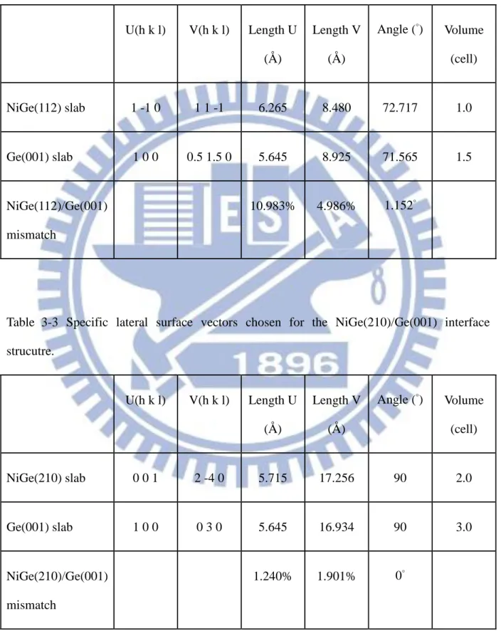
In constructing the NiGe/Ge interface structure, we must match the lattice constants of the two materials along the interface by choosing a suitable in-plane cell size that provides enough calculation accuracy by consuming a reasonable amount of computing resource. The two lateral surface vectors U and V on the above interface plane are shown in Table 3-2, 3-3,
36
and 3-4, for different NiGe surface orientations. The above mentioned cell shapes is mapped on the Ge(001) surface, as illustrated in Figure 3-6. Given that the Ni-Ge metallic bond is weaker than the covalent Ge-Ge, the NiGe slabs are relaxed to match the fixed lateral cell size of Ge(001) slabs. Following the above procedures and considerations, we can successfully construct the NiGe(112)/Ge(001), NiGe(210)/Ge(001), and NiGe(111)/Ge(001) interface structures.
Nevertheless, the cell size of the NiGe(210)/Ge(001) and NiGe(111)/Ge(001) interface structures are too large beyond our computability to calculate the electronic structures using HSE06 functional. Hence, the realistic polycrystalline NiGe film is represented for the subsequent calculations by merely considering NiGe(112) phase, which is the highest diffraction peak in the XRD analysis of NiGe film.
There are two different surface terminations of the NiGe(112) slab, as shown in Figure 3-7 and 3-8, respectively. One of the termination types, hereby called NiGe(112)T4 slab, contains 4 atoms (2 Ni and 2 Ge atoms) per lateral unit cell, while the other type, NiGe(112)T8, has 8 atoms (4 Ni and 4 Ge atoms).
To compare the stability of not only the two termination types but also by sliding NiGe and Ge slabs along the interface, we put the NiGe and Ge slabs together with various choices of lateral matching for both terminations, as shown in Figure 3-9. The total energies of all the configurations we tried are separately listed in Table 3-5 and Table 3-6.
The results in Table 3-5 show that the NiGe(112)/Ge(001) interface structure becomes the most stable when the NiGe slab is terminated at the above-mentioned T4 with the Ni of NiGe being matched to the Ge of Ge(001). This particular configuration of the NiGe/Ge interface structure will be used all though the rest of this thesis.
![Table 1-1 Material characteristics of alternative channel materials [10]. ...........................](https://thumb-ap.123doks.com/thumbv2/9libinfo/8748620.205413/13.892.142.821.351.943/table-material-characteristics-alternative-channel-materials.webp)

![Table 1-1 Material characteristics of alternative channel materials [10].](https://thumb-ap.123doks.com/thumbv2/9libinfo/8748620.205413/28.892.120.809.192.929/table-material-characteristics-alternative-channel-materials.webp)
![Figure 1-3 Schematic representation of source/drain structure and series resistance components [3]](https://thumb-ap.123doks.com/thumbv2/9libinfo/8748620.205413/30.892.126.801.148.997/figure-schematic-representation-source-structure-series-resistance-components.webp)
![Figure 1-5 Schematic band diagram of band bending according to the Schottky-Mott model of the metal/n-type semiconductor: (a) Before contact and (b) after contact formation [26]](https://thumb-ap.123doks.com/thumbv2/9libinfo/8748620.205413/31.892.131.803.152.958/figure-schematic-diagram-according-schottky-semiconductor-contact-formation.webp)
![TraditionalMLCalgorithmsmainlytacklethebatchMLCproblem,wheretheinputdataarepresentedinabatch[24,28].Nevertheless,inmanyMLCapplicationssuchase-mailcategorization[22],multi-labelexamplesarriveasastream.Onlineanalysisistherefore dimensionreducermotivatedbyma](data:image/gif;base64,R0lGODlhAQABAIAAAP///wAAACH5BAEAAAAALAAAAAABAAEAAAICRAEAOw==)