國 立 交 通 大 學
機 械 工 程 學 系
博 士 論 文
高介電閘極層,間隙層構成,與矽鍺磊晶之製程
研發以強化 CMOS 效能
Process development on high-k gate stack,
spacer formation and SiGe growth for CMOS
performance enhancement
研 究 生
: 鄭 博 倫
指導教授 : 徐 文 祥 博士
高介電閘極層,間隙層構成,與矽鍺磊晶之製程
研發以強化 CMOS 效能
Process development on high-k gate stack, spacer formation
and SiGe growth for CMOS performance enhancement
研 究 生︰鄭博倫 Student︰Po-Lun Cheng
指導教授︰徐文祥 Advisor︰Wensyang Hsu
國 立 交 通 大 學
機 械 工 程 學 系
博 士 論 文
A Dissertation
Submitted to Department of Mechanical Engineering
College of Engineering
National Chiao Tung University
in Partial Fulfillment of the Requirements
for the Degree of
Doctor of Philosophy
in
Mechanical Engineering
Dec 2008
Hsin-Chu, Taiwan
中華民國九十七年十二月
高介電閘極層,間隙層構成,與矽鍺磊晶之
製程研發以強化 CMOS 效能
學 生 ︰ 鄭 博 倫 指 導 教 授 ︰ 徐 文 祥
國立交通大學機械工程學系 博士班
摘 要
本篇論文提出半導體前段重要的三項製程技術之改善方案,包括高介電閘 極結構製程,間隙層製程,以及矽鍺薄膜的沉積,前兩項製程技術可用來改善 N 型及 P 型金屬氧化層半導體的效益,第三項技術主要是可改善 P 型金屬氧化層半 導體的效益。 在高介電閘極結構形成部分,在此提出一個結合高介電材料及金屬電極的 整合性製程,以降低漏電流及電性氧化層厚度。此外,根據這個流程,可達到雙 功函數金屬閘極的功能。 間隙層的製程改善部分,因為乙矽烷對溫度的低敏感度,在此提出用乙矽 烷取代習用的矽烷來作為形成間隙層的原料,結果顯示可以改善薄膜沈積的均勻 度達 68% 及改善電流均勻度約 9% ,並可同時提昇生產量及降低熱預算。 在沉積矽鍺薄膜的處理技術上,主要是在矽鍺薄膜沈積前,使用循環式的 臭氧/氫氟酸清洗流程、低溫的氯化氫烘烤以及矽薄膜的沈積等前處理方法,用 以沈積出低缺陷的矽鍺薄膜。實驗結果顯示,以此新製程所沉積的矽鍺薄膜可以 提供約 2.4 倍的電洞遷移速率。也因為矽鍺薄膜提供了區域性壓應力而強化了 電洞遷移速率,以及利用硼的摻雜技術來有效降低接觸電阻,所以可以進一步提 升 P 型金屬氧化層半導體的電洞速率達 32%。Process development on high-k gate stack,
spacer formation and SiGe growth for CMOS
performance enhancement
Student : Po-Lun Cheng Advisor : Wensyang Hsu
Department of Mechanical Engineering,
National Chiao Tung University
Abstract
In this work, gate stack formation for high-k materials, spacer process improvement and stress enhancement process before SiGe growth are proposed. The first two processes can improve the performance of pMOSFET and nMOSPET, and the third process can improve the pMOSFET performance.
In gate stack formation, one feasible process flow integrating high-k and metal gate to decrease Jg (gate leakage) and EOT (electrical oxide thickness) without further
impacting mobility is proposed, where dual work function metal gate can be formed by the proposed flow.
For spacer process improvement, instead of using conventional silane-based nitride, disilane-based nitride is proposed to use on spacer here, since the disilane precursor is non-sensitive to temperature. The experimental results show the improvements on thickness uniformity by 68% anduniformity onIdsat variationby 9%.
The throughput enhancement and thermal budget reduction are also achieved.
In SiGe growth, an improved pre-treatment process is proposed by performing
cyclical O3/DHF clean, low temperature HCl bake and Si seed growth prior to SiGe
growth. Then the in-situ boron-doping SiGe is deposited with dislocation free. It is shown that hole mobility is enhanced around 2.4 times. Furthermore, combined effects from enhanced mobility provided by compressive local stress and in-situ boron doping to decrease contact resistance contribute the Ion gain enhancement around 32%
Acknowledgments
I deeply appreciate my advisor, Dr. Wensyang Hsu, for his patient guidance on my research during the past years. Dr. Wensyang Hsu teaches me the correct research method which be useful for my future research.
The project supported from UMC is acknowledged. Thanks my company’s managers Dr. Chan Lon Yang and Dr. Chin Cheng Chien for their great support, and thanks Chin I Liao, Pin Chien Chu and Ted Guo of UMC for their process assistance. Also, the staffs at device group of UMC are greatly appreciated for providing electrical results and analysis.
I want to express my heartfelt thanks to my parents for their love and support during my education. Thanks my wife, Shin Wen Chou, for her encouragement in my research life. And thanks my son, Jun Yo Cheng, he made my life more colorful. Finally, I would like to thank all people have ever helped me.
Contents
Abstract ( in Chinese )
i
Abstract ( in English )
ii
Acknowledgments
iii
Contents
iv
List for Tables
vii
List for Figures
viii
Chapter
1
INTRODUCTION
1
1.1
Motivation
1
1.2
Previous
Research
3
1.2.1 Gate Approach
3
1.2.2 Spacer Materials
5
1.2.3 Stress Engineering
6
1.3
Current
Approach
7
1.3.1 High-K and Metal Gate
7
1.3.2 Disilane-based Spacer
8
1.3.3 SiGe Epitaxial Growth on pMOSFET
9
Chapter 2 PRINCIPLES
11
2.1 Electrical Thickness
11
2.2 Spacer Process
13
2.3 Stress Enhancement
14
Chapter 3 PROCESSES of FABRICATION
18
3.1.1 High-K and Metal Gate
18
3.1.2 Spacer Process
19
3.1.3 SiGe Process
20
3.2 Process Flow
23
3.2.1 Front-End Process
23
3.2.2 High-K and Metal Gate
23
3.2.3 Spacer Formation
26
3.2.4 SiGe Growth
26
Chapter 4 RESULTS
30
4.1 Spacer Process
30
4.1.1 Physical Results
30
4.1.1.1 Thickness Uniformity
30
4.1.1.2 Dry and Wet Etch Rate
31
4.1.1.3 Surface Roughness
31
4.1.1.4 Pattern Loading Effect
32
4.1.1.5 Discussion
33
4.1.2 Electrical Results
35
4.2 SiGe Process
36
4.2.1
Physical
Results
36
4.2.1.1
Pre-clean
Challenge of Structured Wafers
36
4.2.1.2 Low Temperature Chemical Bake
37
4.2.1.3 Effect of Pre-epi DHF Clean Time
38
4.2.1.4 Cyclical Wet Clean in DIW-O
3/SC1/DHF
40
4.2.1.5 Si Seed Growth
41
4.2.1.6
Discussion
45
Chapter 5 CONCLUSION
55
5.1 Summary
55
5.1.1 High-K Process
55
5.1.2 Spacer Process
55
5.1.3 SiGe Process
56
5.2 Future Works
57
Reference
59
List for Tables
Table 1. Temperature versus activation energy for disilane and silane-based
List for Figures
Figure 1. Front-end processes: Gate stack, Recessed SiGe growth and Spacer
formation 2 Figure 2. Gate film stack for: (a). traditional SiO2 with poly gate; (b). High-K with
metal gate 11
Figure 3. Gate depletion effect in the inversion region 13
Figure 4. Lattice structures of strained SiGe and relaxed SiGe 15
Figure 5. Stress relation for Ge concentration and recess depth 16
Figure 6. Resistance saturation curve 16
Figure 7. Critical thickness curve for different Ge concentration 17
Figure 8. ALD process sequence 19
Figure 9. Revolution scheme with Si seed layer and TEM view of pMOSFET with
SiGe 21
Figure 10. Methods for SiGe pre-treatment 22
Figure 11. Integration issue: (a). poly bmp; (b). selective loss 23
Figure 12. Front-end process flow 24
Figure 13. Novel process flow to integrate high-K & metal gate 27
Figure 15. Flow of SiGe process 29 Figure 16. Based on the same thickness, the range comparison of disilane and silane
nitride on blanket wafer 31
Figure 17. Dry etch rate and wet etch rate 32
Figure 18. Roughness comparison 32
Figure 19. Temperature versus growth rate for disilane and silane-based nitride 34
Figure 20. Idsat variation 36
Figure 21. SIMS profiles of C, O and Ge in SiGe epitaxial films grown (a) after H2
bake alone and (b) after HCl bake and H2 bake 39
Figure 22. (a) Shorter time for HCl bake and (b) longer time for HCl bake 39
Figure 23. Top view SEM images of selective SiGe epi film after (a) shorter and (b)
longer DHF clean time 40
Figure 24. Top SEM images of selective SiGe epi deposited after (a) one cycle of
DIW-O3/SC1 clean and (2) multi-cycles of DIW-O3/SC1. Total HF time
was the same 41
Figure 25. Cross-sectional TEM images of selectively grown SiGe epi in recessed Si
after (a) one cycle and (b) multi-cycles of O3-DI/SC1/DHF clean 41
Figure 26. XTEM comparison of selectively grown SiGe film (a) with and (b) without
Figure 27. XTEM comparison of selectively grown SiGe film (a) without and (b) with
Si seed 43
Figure 28. SiGe roughness (a) with and (b) without Si seed 43
Figure 29. SIMS profile (a) SiGe:B film with Si seed, (b) boron profile comparison
between SiGe:B film with and without Si seed 45
Figure 30. Selective epitaxy process 46
Figure 31. Vth vs. Lpoly. SCE is improved by Si seed 49
Figure 32. pFet Ion-Ioff characteristics. A 32% Ion current gain is achieved
@Ioff=100nA/um 50
Figure 33. pFet I-V characteristics: (a). Ion versus Vt, (b). Ioff versus Vt 51
Figure 34. pFet current characteristics: Ioff versus Idlin 51
Figure 35. Mobility improvement by SiGe film 52
Figure 36. Comparison of non-salicide resistance 53
Figure 37. Comparison of area junction area capacitance 53
Figure 38. Comparison of overlap capacitance 54
Figure 39. Comparison of junction sidewall gate capacitance 54
Chapter 1 INTRODUCTION
1.1 Motivation
Shrinking the conventional MOSFET (metal-oxide-semiconductor field-effect transistor) beyond the 45nm technology node requires innovations to overcome barriers of basic physics. Hence lots of methods for improvement of CMOS performance are proposed already. The methods include (1). Gate stack develop to increase dielectric constant by using nitrided oxide, high-k materials, or metal gate. (2). Device uniformity improvement by spacer material selection. (3). Stress engineering can improve nMOSFET by tensile stress film and pMOSFET by compressive stress film. (4). USJ (ultra shallow junction) optimization. In this work, gate stack, spacer formation and stress enhancement are discussed. Gate stack
approach implemented high-k and metal gate to decrease Jg (gate leakage) and EOT
(electrical oxide thickness) without impacting mobility further. Spacer material selection relates to device uniformity and thermal budget reduction. A recessed source and drain SiGe application is performed to increase Idsat (saturate drain current) with
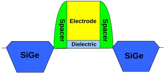
lower contact resistance and enhance mobility by stress enhancement. These three front-end processes are applied to improve device performance, and simple transistor with these three processes is showed in Figure 1.
SiGe
SiGe
Dielectric ElectrodeSpacer
Spacer
SiGe
SiGe
Dielectric ElectrodeSpacer
Spacer
Figure 1. Front-end processes: Gate stack, Recessed SiGe growth and Spacer formation
For gate approach, nitrided oxide will not meet advanced device request in the near future due to the limitation of dielectric constant. The high-k materials, which mean the materials with high dielectric constant, will be the mainstream to thin down electrical thickness continuously. Besides, metal gate instead of traditional polysilicon gate is also the trend to improve device performance by implementing the different work function in nMOSFET and pMOSFET respectively. The high-k materials, like Al O (aluminum oxide), HfO (hafnium oxide) and HfSiO (hafnium silicate), are used widely. And the metal gate materials contain TiN (
2 3
titanium nitride) and TaN (tantalum nitride). However, no matter which materials we choose for dielectric and electrode layer, the process integration issue should be overcome due to cross-contamination concern and post thermal budget considerations. Here we propose a novel process flow to solve these issues.
Once the device generation scales down to the 65nm node or beyond, thermal budget is a concern for high performance devices, but from a manufacturing viewpoint, low throughput cannot be tolerated. Unfortunately, low thermal budget and low throughput is often a trade-off for the CVD process. In addition to thermal budget and throughput consideration, temperature sensitivity is also considered since it is
related to process stability and uniformity. In particular, silicon nitride film is applied widely on different layers of the CMOS process, such as pad nitride, hardmask, and spacer. Once silicon nitride is used in spacer layer, the thickness non-uniformity maintenance will be an important task to obtain good device performance of characteristics such as Ion and overlap capacitance. Here we propose disilane-based
nitride compared with silane-based nitride to obtain good within-wafer uniformity control using a single-wafer tool. It has the characteristics of low thermal budget, insensitivity to temperature, and throughput is comparable with a furnace tool.
For stress engineering, locally strained Si technology using embedded SiGe has demonstrated to improve pMOSFET device performance through hole mobility enhancement. Widely used, embedded SiGe is achieved by selectively growing epitaxial SiGe film in recessed Si pMOSFET source and drain areas. Good device performance gain relying on high quality SiGe film growth, which includes growth surfaces free of damage and chemical contaminants. Non-ideal surface conditions lead to film nucleation difficulties and prevent smooth film growth in mild cases and film growth in severe cases. Once non-ideal film is formed, the dislocation or stacked defect will result in electrical performance degradation, like high leakage, low hole current, and SCE (short channel effect). Here there are two development approaches about the SiGe layer. One is pre-treatment technology prior to epitaxial SiGe growth since the epitaxial growth is sensitive to surface condition, and the other will be focused on SiGe film characteristics.
1.2 Previous Research
1.2.1 Gate Approach
sequentially formed on a substrate, and then the poly-Si layer is patterned into a gate using lithography and etching techniques. Thereafter, ion implantation is conducted to form a source/drain region in the substrate beside the gate.
The conventional film stack for gate structure is SiO2 (silicon dioxide) with
polysilicon deposited above. Dielectric constant of SiO2 is around 3.9, which can not
meet CMOS successful criteria beyond 90nm technology node [1]. The new materials instead of SiO2 is developed, like Si3N4 (silicon nitride) with dielectric constant
around 7. Even silicon nitride contains ~2X dielectric constant than SiO2, the interface
with Si beneath or polysilicon above is poor. Therefore the compromise method is discussed, like nitrided oxide by nitrogen doping in oxide to increase dielectric constant [1-2]. But for increasing higher dielectric constant, high-K materials (HfO2,
HfSiOx, Al2O3 etc.) are developed.
The conventional material of MOS gates is doped poly-Si. However, poly-Si is not an ideal gate material in advanced processes for having higher resistance. Therefore, metal is currently used to form the gates in many advanced MOS processes to solve the above problem. Unfortunately, a metal gate has a disadvantage that defects are easily produced at the interface between the metal gate and the gate dielectric layer during the etching process of the metal gate. In addition, when devices become smaller, exactly defining a metal gate through metal etching is more difficult.
On the other hand, the integration of metal-gate CMOS process including PMOS and NMOS processes suffers from many problems, such as etching, thermal or contamination issue. Especially, it is hard for NMOS and PMOS devices to maintain their optimal wok functions. Therefore, the performance of the CMOS device cannot be well adjusted [3].
However the new materials (high-K and metal gate) are challenging the promised CMOS process flow because the contamination concern and thermal budget control will make the existed process flow change [4].
1.2.2 Spacer Materials
During the fabrication of the MOSFET, after forming the gate electrode, the offset spacer and/or the spacer, made of silicon oxide or silicon nitride, will be formed on the two sidewalls of the gate electrode in the subsequent processes. Afterwards, ion implantation will be performed to form the LDD structure or the source and drain regions at the two sides of the gate electrode, through the offset spacer or the spacer. For example, a composite silicon oxide/silicon nitride spacer may be formed on the sidewalls of the gate by forming an offset oxide layer and a silicon nitride layer covering the substrate and the gate electrode in sequence and then performing etching to remove a portion of the silicon nitride layer until the offset oxide layer is exposed. During the ion implantation process, the uniformity of the oxide or nitride layer of the offset spacer or the spacer has great impact on the dopant profile or junction profile of the formed LDD structure or even the source/drain region.
However, once the size of the device and the line-width shrink, the margin of thickness variation in each layer also become smaller. Especially if the offset spacer or spacer is made from a non-uniform silicon nitride layer, not only the junction depth of the subsequent doped regions may be diverse, the effective channel length of the gate electrode may also be changed, which significantly affects the reliability and uniformity of the semiconductor devices on the wafer.
Usually, a single-wafer process is applied to reduce the thermal budget instead of using a furnace. This has the advantages of low thermal budget [5] and wider tunable space. However, a furnace can produce a more uniform film than a
single-wafer tool because of good thermal distribution and boat rotating design. Single-wafer tools often show worse within-wafer uniformity than a furnace because the chamber design of a single-wafer tool restricts uniformity improvement. For example, the coil distribution in a heater will lead to poor uniformity of heat flow, and lead to poor thickness uniformity. Besides, the poor uniform coil distribution will get some areas hot and some cold, which are called “cold spots.”
Currently, it is common to employ SiH4 and NH3 as the reactant gases for
forming the silicon nitride layer by the single wafer tools. However, the obtained silicon nitride layer has inferior and unsatisfactory within wafer uniformity, wafer-to-wafer uniformity and lot-to-lot uniformity. Alternatively, furnace can be used to form the silicon nitride layer for the wafers in batch. However, higher thermal budget is required and the production cost is therefore higher.
Many efforts have been made to obtain better within-wafer uniformity with single-wafer tools such as swap heater, tuning the outer/inner power ratio of the heater, and optimizing gas flow path. Since silane is sensitive to temperature variation, it is hard to solve this issue. Hence, a precursor non-sensitive to temperature is beneficial for well control for within-wafer uniformity.
1.2.3 Stress Engineering
Locally strained Si technology using embedded SiGe has demonstrated improved pMOSFET device performance through hole mobility enhancement [6-8]. Widely used, embedded SiGe is achieved by selectively growing epitaxial SiGe film in recessed Si source and drain in the pMOSFET area. Prior to the selective deposition step, device wafers go through usual gate formation, spacer formation, multiple implants (e.g. LDD, halo, and HDD), anneal, etc. Typical process steps and the impact of process sequence for recessed source and drain SiGe application are
described elsewhere [7].
Non-ideal surface conditions lead to film nucleation difficulties and prevent smooth film growth in mild cases and film growth in severe cases. Surface chemical contaminants are typically removed by wet clean and high temperature bake prior to epi deposition. For example, diluted HF (DHF) is used to remove native oxide and passivate the surface from further contamination. However, the DHF clean also removes protective layers (e.g. oxide hardmask) over pMOSFET gates and nMOSFET areas required for selective deposition, and the clean time is limited to the chemical budget of the wafer structure. Pre-epi high temperature bake (>850°C) is commonly used [9-10] to effectively remove interface contaminants (C and O) between epi film layer and Si substrate, however, the bake temperature cannot exceed the thermal budget of the device wafer. Besides, Si migration is a concern for high temperature bake. Such chemical and thermal budgets impose a small pre-clean window and challenges for both wet and dry cleaning of surfaces with accumulated damage and chemical residues.
When SiGe layers are grown epitaxially on Si substrate, the stress is relaxed by plastic deformation, i.e., misfit dislocations are formed when the strain in the layers exceeds the critical thickness or germanium concentration. Many researches pay attention on this field to grow the good quality SiGe film and prevent stress relaxation due to the dislocations [11].
1.3 Current Approach
1.3.1 High-K and Metal Gate
sacrificial layer with two gate openings is formed on a substrate. Next, a gate dielectric layer is formed on the substrate exposed by the first sacrificial layer. Thereafter, a second sacrificial layer is filled in the first and second gate openings. The second sacrificial layer in the first gate opening is removed, and then a first conductive layer is filled in the first gate opening as the gate of a first MOS transistor of a first conductivity type. Then, the second sacrificial layer in the second gate opening is removed. A second conductive layer is filled in the second gate opening as the gate of a second MOS transistor of a second conductivity type, and the first sacrificial layer is removed.
Since the above process of forming gates utilizes a damascene method, rather than a conventional direct-etching method, the quality of the interface between a metal gate and the gate dielectric layer can be improved, and the metal gate can be defined more exactly. Moreover, since the first conductive layer and the second conductive layer can be different, the work functions of PMOS and NMOS can be tuned respectively.
1.3.2 Disilane-based Spacer
Low thermal budget, insensitivity to temperature, and comparable throughput are necessary criteria of spacer process for next generation devices [12-14]. To meet the criteria above, we proposed the precursor – disilane instead of silane to react with NH3 to form nitride film in the single-wafer tool. Since disilane is not sensitive to
temperature, it is easier to control the within-wafer uniformity using nitride film with disilane. Moreover, the mechanism showed disilane has lower activation energy for breaking the Si-Si bond. It also makes better within-wafer uniformity easier to achieve.
Normally, the process with higher temperature has higher throughput, and tends to diffusion-limited reaction, which means less sensitivity to temperature. But it
contains the drawback of higher thermal budget. However, disilane nitride not only controlled in diffusion-limited reaction with lower temperature, but also kept the throughput comparable with silane precursor. And the physical and electrical data of disilane-based nitride is better than silane-based nitride, which will be shown in Chapter 4.
Here, we also propose a method for forming a carbon-containing silicon nitride layer with superior uniformity for spacer application, by low pressure chemical vapor
deposition (LPCVD) using disilane (Si2H6) and ammonia (NH3) and at least one
carbon-source precursor as reactant gases, preferably by single wafer tools but also compatible with furnace processes.
1.3.3 SiGe Epitaxial Growth on pMOSFET
In this study, wafers were processed through a CMOS flow using oxide film to protect nMOSFET areas during selective SiGe epitaxial growth. Multiple implants’ reactive ion etch used in recessed source/drain formation, and PR strip prior to selective epi deposition result in physical damage and chemical residues on the film growth surface. Growth surfaces free of damage and chemical contaminants are required to obtain high quality SiGe epi films.
For delivering the high quality SiGe epi film, we present several cleaning approaches that obtain better interfacial quality and improve SiGe epi film morphology further. One effective method is cyclical wet clean through ozonated DI
water (DIW- O3), SC1, and DHF, and is discussed. The effect of pre-epi DHF clean
time is also explored. Low temperature chemical bake using HCl (g) in H2 carrier gas
is also presented as an effective method to reduce interfacial contaminants and improve epi film morphology.
and limitation of process window, use of a silicon seed layer is employed to nucleate uniform SiGe film with good quality and to minimize the micro-loading effect. Device performance without degradation is also discussed in this paper.
Chapter 2 PRINCIPLES
2.1 Electrical Thickness
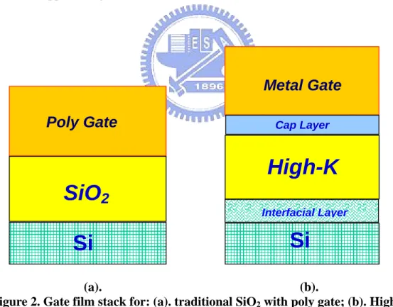
Figure 2 shows the film stack difference between traditional SiO2 with poly gate
and high-K with metal gate. For obtaining better performance, the cap layer (between high-K and metal gate) and interfacial layer beneath high-K are necessary to be considered seriously, but no this kind of issue for traditional SiO2 with poly gate. The
cap layer prevents interfacial reaction and dipole formation, which will degrade electrical performance. And the interfacial layer beneath high-K can prevents interfacial trapped charge and interfacial reaction.
Si
Cap LayerMetal Gate
High-K
Interfacial LayerSi
Poly Gate
SiO
2
(a). (b).Figure 2. Gate film stack for: (a). traditional SiO2 with poly gate; (b). High-K
with metal gate
Based on Eq. (2.1-1) and (2.1-2), Idsat is proportional to C (capacitance). And
Id = (W/L)ℳ C( Vg – Vt – Vd/2 ) Vd (2.1-1)
I d. sat = (W/L)ℳ C(Vg – Vt )2/2 (2.1-2)
C = (k €0 A) / t (2.1-3)
(Id : drain current; I d. sat : saturation drain current;
W : width; L : length;
ℳ : effective mobility; C: capacitance;
Vg : gate voltage; Vt : threshold voltage; Vd : drain voltage;
k : dielectric constant; €0 : permittivity; A : area; t : physical thickness)
We know that dielectric constant of silicon dioxide k oxide = 3.9. For example, if
one kind of high-k dielectric constant k high-k =16 and to achieve the equivalent
capacitance density compared with oxide physical thickness~10A, we can deposit this kind of high-k film~41A. The Eq. (2.1-4) is showed as below:
k oxide / t ox = k high-k / t high-k Æ 3.9/10=16/41 (2.1-4)
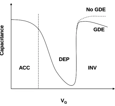
Hence, the advantages of high-k are (1). Keep the same capacitance density even thicker thickness is used; (2). Thicker layer can suppress tunneling current. And the advantages of metal gate are (1). No GDE (gate depletion effect will degrade Id.sat) as
ACC
DEP
INV
Figure 3. Gate depletion effect in the inversion region
2.2 Spacer Process
Normally, the CVD process is a competition reaction between a surface-limited reaction and diffusion-limited reaction. What kind of reaction dominates will affect the ability of process and uniformity control. The formula of surface reaction and
diffusion reaction is shown in Eq. (2.2-1) and (2.2-2), respectively. (K0:
temperature-independent pre-exponential constant; Ea: activation energy; k: Boltzmann constant; T: temperature; Cs: surface concentration; Cg: transfer concentration; D: diffusion constant; d: distance)
Surface reaction: Cs*K0*Exp (-Ea/kT) (2.2-1)
Diffusion reaction: D*(Cg-Cs)/d (2.2-2)
According to Arrhenius theory, for reaction equilibrium, the flux of reactor diffuse to bare wafer surface will be the same. So the formula must be established:
VG Capa c it an ce No GDE GDE ACC DEP INV G Capa c it an ce No GDE GDE V
(Kr: reaction rate constant)
D (Cg-Cs)/d = KrCs (2.2-3)
Cs=Cg/(1+α) (2.2-4)
α=Krd/D (2.2-5)
Higher Ea (activation energy) will result in a small Kr value, and the process
situation becomes Cg=Cs (a traditional surface-limited reaction), which means all the
reactants will accumulate at the surface and thickness will vary rapidly with temperature variation. Otherwise, a precursor with lower Ea will lead the process close to diffusion reaction, which presents the key information: it is non-sensitive to temperature. Generally, a CVD process prefers to dominate by diffusion-limited reaction due to non-sensitivity to temperature. Hence, choosing the precursor with low activation energy is the trend for the CVD process.
Besides, according to the method for forming the carbon-containing silicon nitride layer proposed in this paper, the carbon-containing silicon nitride layer can offer better superior uniformity and high carbon content, when compared with the conventional silicon nitride layer. Furthermore, the carbon in the resultant silicon nitride layer can help trap free hydrogen in the device and prevent boron diffusion exacerbated by free hydrogen [15]. Therefore, due to less free hydrogen and better uniformity, the electrical characteristics of the device are improved.
2.3 Stress Enhancement
Recessed SiGe can provides the compressive stress under gate stack, and improve hole mobility further by changing band gap [16]. The reason of compressive
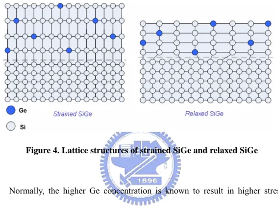
stress provided by SiGe on channel is that Ge have around 4% larger lattice constant than Si. Once strained SiGe is formed by silicon and germanium, the extruded lattice structure will provide the compressive stress. On the other hand, the relaxed SiGe has no stress benefit. These two kinds of lattice structure are shown in Figure 4.
Figure 4. Lattice structures of strained SiGe and relaxed SiGe
Normally, the higher Ge concentration is known to result in higher stress in embedded SiGe, shown in Figure 5. But it is difficult to maintain the stress for a high Ge concentration in recessed SiGe due to the stress relaxation and defect propagation in a highly strained SiGe layer [17]. Moreover, the recess depth is also proportional to stress enhanced by SiGe in Figure 5, but the limitation is necessary to find for different device condition.
Stress Saturation
300 700 900 1100 1300 300 700 900 1100 1300Normalized recess depth
Nor m al iz ed str e ss 2.6 2.2 1.8 1.4 1 0.6 2.6 2.2 1.8 1.4 1 0.6 Increase Ge% 2.2 2 1.8 1.6 1.4 1.2 1 0.8 0.6 0.4 0.6 0.8 1 1.2 1.4 1.6 1.8 2 2.2 0.4
Figure 5. Stress relation for Ge concentration and recess depth
Since the boron is incorporated in SiGe by in-situ process, more boron incorporated is positive for resistance reduction. Besides, more boron incorporated will enhance Ion current. But unfortunately, more boron incorporated will induce more
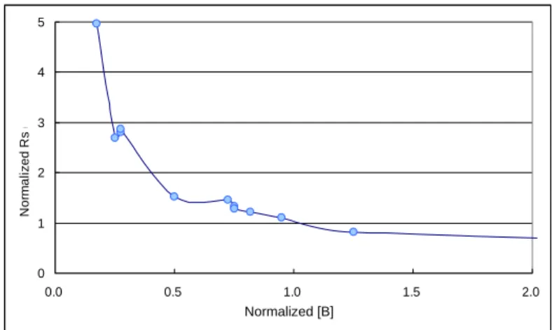
stacked defect in SiGe film, and make boron out diffusion seriously, which will lead to SCE (short channel effect) and degrade electrical performance due to high leakage current. Hence, we need to improve process to maintain the suitable boron concentration to keep the lowest resistance as shown in Figure 6.
0 1 2 3 4 5 0.0 0.5 1.0 1.5 Normalized B] (cm-3) N o rm a li z ed R s ( ohm /s qr 2.0 ) Normalized [B]
As we discussed before, more Ge concentration will obtain more stress, and enhan
Figure
ce Ion current in pMOSFET further. D. C. Houghton mentioned that once the
SiGe thickness is thicker than the critical thickness for the specific process condition, shown in Figure 7 [11], the electrical performance will be degraded due to stress relaxation. Therefore, we can not increase Ge concentration without limitation. The thickness and Ge concentration for different product and layout are necessary to be optimized and prevent stress relaxation.
7. Critical thickness curve for different Ge concentration SiGe TK
Chapter 3 PROCESSES of FABRICATION
3.1 Experimental Design & Considerations
3.1.1 High-K & Metal Gate
The gate dielectric layer comprises HfO2, A12O3, HfSiO, or HfSiON. Besides,
the conductive gate of the PMOS transistor comprises Ru, RuO2, W, TiN or Ru Ta
alloy, and the gate of the NMOS transistor comprises Ta, TaN, TaSiN, TiN or Ru Ta alloy.
The method wherein forming the gate dielectric layer and conductive material comprises an atomic layer deposition process or a metal-organic chemical vapor deposition process.
Whatever we choose which materials we mention above, all these materials are incompatible with current productive CMOS factory since they will contaminate front-end processing tools. Therefore a protocol to prevent the cross-contamination is necessary for high-K and metal materials implement.
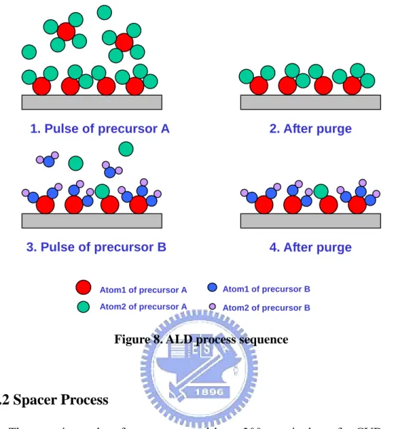
ALD (atomic layer deposition) is a popular method to form ultra thin film with good uniformity. It follows these 4 steps to form very thin layer in Figure 8. Metal precursor (ex. precursor A) pulse and chemisorption in step1, and use N2 to purge the
weak bonding in step 2. In step3, another precursor (ex. precursor B) pulse and react
with the existed precursor (ex. precursor A) to bond each atom together. Then N2
purge the weak bonding again. Hence, the step 1 to step 4 is cyclic and the cyclic number will decide the final thickness.
1. Pulse of precursor A 2. After purge
3. Pulse of precursor B 4. After purge
Atom1 of precursor A Atom2 of precursor A
Atom1 of precursor B Atom2 of precursor B
Figure 8. ALD process sequence
3.1.2 Spacer Process
The experimental wafers are prepared by a 300mm single-wafer CVD reactor operating at reduced pressure. During processing, the wafers were put on a heater, which provided process temperature. The process gas was delivered from a shower-head above the heater. For nitride film deposition, we use silane (SiH4) and
disilane (Si2H6) as the silicon source to compare performance. And NH3 is used as the
nitrogen source. The growth temperature is below 750ºC at reduced pressure.
Disilane and silane are different precursors for nitride film deposition. The uniformity of disilane-based nitride is better than silane-based nitride. To explain this mechanism, we prepared wafers for deposition by separating the different deposition temperatures from 600ºC to 740ºC. We also split another deposition rate for the disilane-based SiN process to check if the activation energy is affected by the different
process condition.
The film morphology and thickness are identified by spectrum ellipsometer and cross-section transmission electron microscopy (XTEM). Atomic force microscopy (AFM) is used to observe the surface roughness. Micro-loading is determined by TEM, and etch rate is calculated by ellipsometer measurement results.
As described before, we can incorporate carbon into nitride layer to improve electrical performance further. The carbon-containing silicon nitride layer can be formed by using disilane (Si2H6), NH3 and at least one carbon-source precursor as the
reactant gases, preferably by LPCVD. For example, the carbon-source precursor can
be selected from the group consisting of TEASAT (triethylarsenate, C6H15AsO4),
Trans-LC (C2H2C12), TCS (trichlorosilane, SiHC13), TMA1 (trimethyl aluminum,
Al(CH3)3),C2H4, C3H6, TEB (triethylborate, B(OC2H5)3), TEPO (triethylphosphate,
PO(C2HSO)3), TDMAT (tetrakis-dimethylamino titanium, Ti[N(CH3)2]4) and the
combinations thereof [18]. Preferably, the obtained silicon nitride layer contains more than 9%, up to about 30% of carbon.
3.1.3 SiGe Process
For obtaining better device performance, the good SiGe growth is very important. If not, the dislocation or bulk defect will make the performance gain degradation or high leakage due to stress relaxation. Prior to discuss good SiGe growth, we need to mention about the surface treatment because good surface condition is the basic factor for good SiGe growth.
The experimental wafers were prepared by a 300mm single-wafer CVD reactor operating at reduced pressure. The process tool contains vacuum load locks to prevent the wafers from being exposed to air prior to processing.
The Ge and boron doping sources are GeH4 and B2H6 respectively, and H2 is
used as the carrier gas. The wafers are treated by diluted DHF clean followed by a low
temperature H2 bake prior to SiGe Epi film growth. The growth temperature is
between 600ºC ~ 750ºC at reduced pressure (5 torr ~ 20 torr) for both Si seed and SiGe. A thin Si seed is deposited in the source/drain region prior to in-situ boron-doped SiGe film growth. The Si seed layer thickness is around 10A~30A, and SiGe thickness is around 800A ~ 1200A with around 15~30% Ge concentration. Figure 9 shows the fabrication flow with evolution scheme (with Si seed layer) and TEM view of pMOSFET with SiGe.
Figure 9. Revolution scheme with Si seed layer and TEM view of pMOSFET with SiGe
The film morphology and thickness are identified by spectrum ellipsometer and cross-section transmission electron microscopy (XTEM). The Ge content, boron
concentration and doping profile in SiGe film are measured using secondary-ion mass spectroscopy (SIMS). Atomic force microscopy (AFM) is used to observe the surface roughness.
For obtaining good SiGe quality, the pre-treatment procedure should be taken carefully to produce the good surface prior to SiGe growth. We listed the four normal contaminates to be removed prior to SiGe growth in Figure 10. Surface contaminates
due to remaining from pre-processes can be removed by wet clean, O2 plasma or H2
baking. For native oxide, wet clean or H2 baking can cover that. However, It is hard to
recover for contaminates beneath Si surface, but we can use re-oxidation by O3 then
remove it by wet clean, like DHF, or removing by HCl etching. Regarding the damage and roughness, we propose the vacuum treat to recover it. All details about these treatments will be discussed later.
Damage & Roughness Surface
Contaminates
Native Oxide Beneath Si
Contaminates
a. High temp. anneal b. Vacuum treat c. O3 oxidize Æ DHF remove a. SPM (metal, polymer,organic) b. SC1 (particle) c. SC2 (metal)
d. O2 flush (polymer, organic) e. H2 bake (polymer, organic, O)
a. DHF b. Vacuum treat c. H2 bake a. O3 oxidize Æ DHF remove b. HCl etch
Figure 10. Methods for SiGe pre-treatment
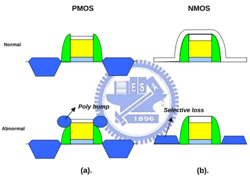
Of course, there are lots of methods to treat surface as well. But once considering to process integration, some limitations will be appeared. For example, a long pre-epi DHF clean may not be realistic for many device structures due to undesirable etching of protective oxide over nMOSFET areas and over pMOSFET
poly. For pMOSEFET, over-etching of oxide film results in poly bump (poly-SiGe) on poly shown in Figure 11-(a), which will made the device bridge. For nMOSFET, over-etching of oxide film results in undesirable SiGe growth on nMOSFET areas, which is called selective loss as shown in Figure 11-(b), during selective SiGe growth process. The maximum allowable DHF clean time or chemical budget of a device structure is set by the etch rates and thicknesses of the protective film layers used in the device structure.
Normal Abnormal PMOS NMOS Poly bump Selective loss (a). (b).
Figure 11. Integration issue: (a). poly bmp; (b). selective loss
3.2 Process Flow
3.2.1 Front-End Process
In this work, these three processes: gate deposition, spacer formation and in-situ boron doped SiGe growth, are discussed. They are belong to front-end processes, and the simple process flow including these three processes is showed in Figure 12.
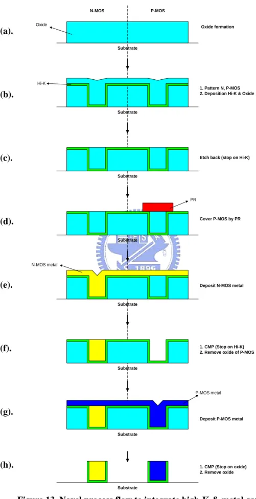
In the following description, the first conductivity type is N-type, and the second conductivity type is P-type.
Referring to Figure 13-(a) and (b), a sacrificial layer (oxide film) is formed on a substrate, with gate openings therein exposing portions of the substrate. It is noted that the thickness of the sacrificial layer is the sum of those of the gate and the gate dielectric layer formed later. Then, a substantially conformal gate dielectric layer (Hi-K, for example) is formed over the substrate. Thereafter, a blanket sacrificial layer is formed over the substrate, covering the gate dielectric layer and filling the gate openings at least. Gate deposition Spacer formation S/D Engineering Recess in S/D region of pFET
In-situ boron doped SiGe Epi growth
Implant Implant Gate deposition Spacer formation S/D Engineering Recess in S/D region of pFET
In-situ boron doped SiGe Epi growth Gate deposition
Spacer formation
S/D Engineering
Recess in S/D region of pFET
In-situ boron doped SiGe Epi growth
Referring to Figure 13-(c), the blanket sacrificial layer outside the gate openings is removed to form a sacrificial layer. The removing method is, for example, chemical mechanical polishing or etching-back. Then, in Figure 13-(d), a mask layer (photo resist layer) is formed to cover the sacrificial layer in the gate opening and then removing the sacrificial layer not covered by the mask layer.
Referring to Figure 13-(e), after the mask layer is removed, a conductive layer as the gate material of NMOS is formed on the substrate, filling the gate opening at least. Referring to Figure 13-(f), the conductive layer outside the gate openings is removed by chemical mechanical polishing or etching-back to form an NMOS gate. Then, another mask layer is formed to cover the NMOS gate in the gate opening and then removing the sacrificial layer not covered by the mask layer.
Referring to Figure 13-(g), after the mask layer is removed, a conductive layer as the gate material of PMOS is formed on the substrate, filling the gate opening at least. Then, in Figure 13-(h), the conductive layer outside the gate openings is removed to form a PMOS gate. Then, the sacrificial layer is removed after the gate dielectric layer thereon is removed, leaving a portion of the gate dielectric layer. The removing method is, for example, a dry or wet etching method. After the gates are formed, the sources/drains of NMOS and PMOS can be formed as usual to complete the CMOS process.
Since the present invention utilizes the damascene technology to form the gates of different work functions, the quality of the interface between a metal gate and the gate dielectric layer can be improved, and the metal gate can be defined more exactly. In addition, since the materials of the NMOS gate and the PMOS gate can be different, the work functions of the NMOS gate and the PMOS gate can be tuned respectively,
so that the performance of the CMOS device can be improved [19].
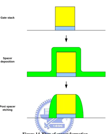
3.2.3 Spacer Formation
Before spacer formation, gate stack is defined first. Then the offset spacer and/or
about the embedded SiGe growth. Therefore, recessed Si in source
the spacer materials, made of silicon oxide or silicon nitride, will be deposited on the two sidewalls of the gate electrode in the subsequent processes. Afterwards, usually dry etch will be performed to form the spacer shape, which remaining thickness is used to define the LDD or the source and drain implant regions at the two sides of the gate electrode. The process sequence is shown in Figure 14.
3.2.4 SiGe Growth
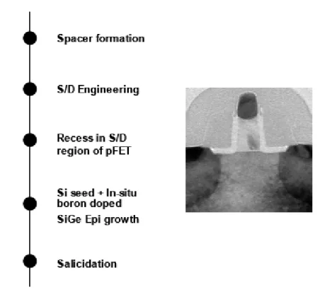
Here we discussand drain area is necessary prior to selectively grow epitaxial SiGe film. As we mentioned before, SiGe growth is sensitive to surface condition. Hence, improved pre-treatments (both treat surface and reduce HM loss in PMOS & cap loss in NMOS) will relate to SiGe film quality. Afterwars, for SiGe growth, we need to consider the SiGe critical thickness and growth conditions to prevent dislocation propagation due to post thermal steps or non-optimized growth conditions. The process sequence is shown in Figure 15.
Figure 13. Novel process flow to integrate high-K & metal gate
Substrate
N-MOS P-MOS
Oxide formation
1. Pattern N, P-MOS 2. Deposition Hi-K & Oxide
Etch back (stop on Hi-K)
Oxide
Hi-K
Cover P-MOS by PR
Deposit N-MOS metal
1. CMP (Stop on Hi-K) 2. Remove oxide of P-MOS
PR Substrate Substrate Substrate Substrate Substrate Substrate Substrate N-MOS metal P-MOS metal
Deposit P-MOS metal
1. CMP (Stop on oxide) 2. Remove oxide (a). (b). (c). (d). (e). (f). (g). (h).
Gate stack
Post spacer etching Spacer deposition
SiGe growth Pre-SiGe
clean Post recess
etching
Chapter 4 RESULTS
4.1 Spacer Process
4.1.1 Physical Results
4.1.1.1 Thickness Uniformity
First, we compare the thickness uniformity between disilane-based and silane-based nitride, including as-deposited and post-etching. Figure 16 shows the 49-point thickness map of nitride film. In Figure 16-(a), the silane-based nitride shows worse uniformity than disilane nitride shown in Figure 16-(b), and Figure 16-(a) shows a special area, which can be called a “cold spots” of the heater. But disilane does not show the cold spot area since it is not sensitive to temperature. Hence, the uniformity of a blanket wafer can be improved by using disilane nitride instead of silane in the range of 1.6 nm to 0.5 nm. The thickness uniformity of the device wafer also shows that disilane-based nitride can be improved about 68% on measurement pads. Since disilane is non-sensitive to temperature, the within-wafer uniformity is independent of tool effects such as heater type and gas flow path. Otherwise, post etch uniformity is more important than as-deposited uniformity since the device is related to post etch profile and uniformity directly. Hence, the dry etch rate and wet etch rate are present in the two following sections.
(a). Silane-based SIN (b). Disilane-based SIN
Figure 16. Based on the same thickness, the range comparison of disilane and silane nitride on blanket wafer
4.1.1.2 Dry and Wet Etch Rate
The dry etch rates of disilane nitride and silane nitride are 12.2nm/min and 15nm/min, respectively. For SPM, the wet etch rates of disilane nitride and silane nitride are 0.88nm/min and 1.5nm/min, respectively. The etch rate is shown in Figure 17. The lower etch rate for dry and wet etch of disilane nitride is beneficial to controlling the uniformity, and to increase the etching process window at the same time, especially once this kind of film is applied on the spacer layer. Furthermore, the map measured by SCD (spectrum CD) also showed the within-wafer range of disilane nitride was improved 32%.
4.1.1.3 Surface Roughness
Generally, lower activation energy means higher growth rate, which might lead to a rougher surface. For the accepted temperature, the growth rate is 10.7nm/min and 8.6nm/min for disilane-based and silane-based nitride, respectively. But the AFM results show disilane-based nitride can obtain comparable roughness to silane-based nitride. Figure 18 shows the roughness results.
15 1.5 0.88 12.2 0 2 4 6 8 10 12 14 16 18
Silane Nitride Disilane Nitride Film
Dry etch rate Wet etch rate
Figure 17. Dry etch rate and wet etch rate
0.15 0.177 0.12 0 0.05 0.1 0.15 0.2 0.25
Silane Nitride Disilane Nitride (recipe1) Disilane Nitride (recipe 2) RM S ( n m )
Figure 18. Roughness comparison
4.1.1.4 Pattern Loading Effect
Here micro-loading was defined as (maximum thickness - minimum thickness) / (minimum thickness) in the same die. Normally, a dense area results in minimum thickness, and an iso area results in maximum thickness. Naturally, decreasing deposition rate can improve micro-loading. In this work, we find that even decreasing deposition rate will not suffer the activation energy, which means within-wafer uniformity won’t suffer. Consequently, we can improve micro-loading effect and
uniformity at the same time. The micro-loading of disilane nitride is improved about 8% compared to silane nitride if the gas flow is fine tuned by disilane. On the contrary, if we decrease the deposition rate of silane nitride to improve micro-loading, throughput suffers seriously.
On the other hand, morphology is a concern because lower activation energy means higher growth rate, which might lead to a rougher surface [20]. But surface roughness was verified by AFM methodology. The results show that disilane-based nitride can obtain comparable roughness to silane-based nitride even though it has a higher growth rate.
The physical data show within-wafer uniformity with disilane nitride can be improved 68% over silane-based nitride. Furthermore, micro-loading was improved 8% by disilane gas.
4.1.1.5 Discussion
Figure 19 and Table 1 show that a disilane-based SiN process has low activation energy, which makes the reaction close to a diffusion-limited reaction. On the contrary, silane-based SIN showed a sharp slope in the same temperature period, which means it has larger activation energy. Disilane-based SiN has smaller activation energy than silane-based SiN in these temperature periods, meaning that disilane-based SiN comes closer to diffusion-limited reaction than silane-based SiN.
Figure 19. Temperature versus growth rate for disilane and silane-based nitride
Nitride Recipe Heater Temperature
(Degree C) Activation Energy (eV) > 650 0.2592 < 650 0.6685 > 650 0.2896 < 650 0.6969 > 690 1.5024 < 690 1.9984
Disilane Nitride (recipe1)
Disilane Nitride (recipe2)
Silane Nitride
Table 1. Temperature versus activation energy for disilane and silane-based nitride
Whether the higher growth rate (disilane 1) or lower growth rate (disilane 2) is used, it always keeps the similar activation energy and slope. It reveals that growth rate does not affect the activation energy for the same precursor, and it is very important for process tuning because the micro-loading phenomena can be improved by decreasing the deposition rate.
dominated by diffusion-limited reaction. We can conclude it has a slower slope compared with silane nitride in Figure 19. The growth rate and thermal budget are acceptable for the 65nm node or beyond.
Naturally, the non-sensitivity to temperature will prevent cold spots on the heater. This means disilane-based nitride is heater independent.
Of course, we can improve the silane-based nitride uniformity if we increase the deposition temperature to approach a diffusion-limited reaction, but it will suffer the thermal budget for the same uniformity target. Decreasing the thermal budget is the future trend of advanced manufacturing. Consequently, it is necessary to search a low activation energy precursor. In our experiment, disilane recipe 1 and recipe 2 have different growth rates, but present the same curve in Figure 19 and similar activation energy in Table 1. The results are beneficial for micro-loading tuning since we can decrease micro-loading effect by tuning its growth rate.
In the results section, we understand that micro-loading can be improved 8% once we modify the gas flow to lower down growth rate. Even so, the characteristic of non-sensitivity to temperature still exists. Normally, lower growth rate decrease pattern sensitivity due to increased gas phase diffusion length [21], which also explains the reason why the micro-loading is minimized.
Disilane is a better precursor for nitride film deposition than silane because it can be controlled on the specific area shown in the top-right corner in Figure 19. Disilane has the characteristics of low thermal budget, comparable throughput, and is non-sensitive to temperature.
4.1.2 Electrical Results
the precision of the implant and channel length control. So, once the disilane-based nitride was implemented on the spacer, the electrical performance improved. For
electrical performance, overlap capacity variation improved 3%, and Idsat improved
9% (shown in Figure 20, which is beneficial for mass production because it allows fabs to deliver high quality and a stable production line. And yield is comparable with these two films.
0.85 0.9 0.95 1 1.05 1. 1 1.15 1. 2 .01 .1 1 5 10 20 30 50 70 80 90 95 99 99. 9 99.99
PFET Idsat Uniformity Compariosn
FilmA Idsat FilmB Idsat Normalize Idsat Pe rc e n t
Item Film A (Silane SIN) Film B (Disilane SIN)
Variation : 3*Sigma/Median 26.5% 17.4% Uniformity : (Range/2)/Median 14.3% 10.9% 0.85 0.9 0.95 1 1.05 1. 1 1.15 1. 2 .01 .1 1 5 10 20 30 50 70 80 90 95 99 99. 9 99.99
PFET Idsat Uniformity Compariosn
FilmA Idsat FilmB Idsat Normalize Idsat Pe rc e n t
Item Film A (Silane SIN) Film B (Disilane SIN)
Variation :
3*Sigma/Median 26.5% 17.4% Uniformity :
(Range/2)/Median 14.3% 10.9%
Figure 20. Idsat variation
4.2 SiGe Process
4.2.1 Physical Results
4.2.1.1 Pre-clean Challenges of Structured Wafers
Pre-epi surface preparation of structured wafers processed through multiple implants and source/drain recess etch is challenging. Complete elimination of residual
implant damage and process-related chemical residues is difficult to achieve without aggressive wet clean or high temperature bake. As a test, one blanket wafer and one structured wafer were subject to diluted HF (DHF) clean followed by a low temperature H2 bake prior to SiGe epi film deposition. Due to process history and accumulated chemical residues (e.g. in recess etch), the structured wafer was first cleaned in ozonated DI water followed by SC1 before the DHF dip. SIMS measurements indicated that while integrated C and O levels at the Si-SiGe interface was maintained at 7×1011 cm-2 and 3×1012 cm-2, respectively, on the blanket wafer, both C and O doses on the recessed wafer exceeded 1013 cm-2.
4.2.1.2 Low Temperature Chemical Bake
g structured wafers, a new low tempe
and O as well as Ge in epitax
ere processed by Due to additional difficulties with cleanin
rature bake process beside the commonly used pre-epi H2 bake was developed.
Prior to SiGe deposition, device wafers were dipped in DHF and were introduced to the epi reactor in a flow of HCl, a reactant gas, and H2 carrier gas. The HCl based
chemical bake step was found to remove top Si surface containing damage and contaminants. As a result, employment of the HCl based chemical bake lowered the interfacial C and O on the recessed S/D growth surfaces.
Figure 21 shows SIMS profiles of interface C
ially grown SiGe films (a) after H2 bake alone and (b) after HCl bake followed
by the H2 bake. The first to note is lowering of C and O peak concentrations by an
order of magnitude at the Si-SiGe interface. Uniform Ge profile was observed in the SiGe grown after the HCl chemical bake while Ge pileup at the interface was observed at the Si-SiGe growth interface without the chemical bake.
the sa
ommonly performed to remove native
due to unde
me epi condition, but with different HCl treatment time. Figure 22 shows HCl can recover surface condition once time and flow are tuned well. Figure 22-(a) shows shorter HCl bake time does not produce good epi near poly sidewall, but Figure 22-(b) shows HCl bake can work, once HCl bake time conditions are fine tuned.
4.2.1.3 Effect of Pre-epi DHF Clean Time Pre-epi clean in DHF prior to epi deposition is c
oxide and contaminants on the growth surface. The DHF clean also serves surface as a hydrogen passivation layer to prevent further contamination. Therefore, optimization of pre-epi HF dip time is critical in achieving an interface with minimal contaminants. In addition to residual contaminant reduction, our study reports that longer DHF clean further prepares the growth surface to improve epi film morphology. Two structured wafers were prepared in DHF for different clean time followed by low temperature HCl based chemical bake and SiGe epitaxial film deposition. SIMS results indicate residual C and O at the Si-SiGe interface were already reduced to below 1018 cm-3 and 1019 cm-3, respectively, after DHF clean. Besides, additional DHF clean did improve SiGe epi film quality. Figure 23 compares the top view SEM images of the two samples prepared by different DHF clean time. SiGe film grown after shorter DHF clean time showed dimpling and uneven morphology while the film grown after double DHF clean time showed much smoother film morphology.
A long pre-epi DHF clean may not be realistic for many device structures
sirable etching of protective oxide over nMOSFET areas. Over-etching of oxide film results in undesirable SiGe growth on nMOSFET areas during selective SiGe growth process. The maximum allowable DHF clean time or chemical budget of a device structure is set by the etch rates and thicknesses of the protective film layers used in the device structure.
Figure 21. SIMS profiles of C, O and Ge in SiGe epitaxial films grown (a) after H2 bake alone and (b) after HCl bake and H2 bake
Figure 23. Top view SEM images of selective SiGe epi film after (a) shorter and (b) longer DHF clean time
4.2.1.4 Cyclical Wet Clean in DIW-O3 /SC1/DHF
An alternative pre-epi surface preparation to a long DHF clean is multiple
cyclical cleaning through a DIW-O3/SC1/DHF sequence. The combination of
DIW-O3 and SC1 removes organic residues and particles while oxidizing the Si
surface. By repeating cycles of surface oxidation in DIW-O3/SC1 and oxide strip in
DHF, effective surface preparation was achieved for epitaxial film growth. Figure 24 compares the morphology of selectively deposited SiGe after (a) one cycle and (b)
multi-cycles of O3-DI/SC1/DHF wet clean with the same total DHF time. Significant
improvement of surface morphology is shown in Figure 24-(b) obtained after multi-cycles of cleaning while Figure 24-(a) obtained after one cycle of cleaning showed dimpling along on the gate/spacer side.
Multiple cycles of DIW-O3/SC1/DHF clean also resulted in more consistent film
growth rates over different recessed areas of various sizes. Figure 25 shows cross-sectional TEM images of SiGe grown in two opening sizes on the surfaces prepared by (a) one cycle and (b) multi-cycles of clean. The wafer cleaned with one cycle showed substantially thinner (30% less) SiGe in the smaller opening compared to the larger opening within the imaged area while the wafer cleaned with
multi-cycles showed no difference in thickness.
Figure 24. Top SEM images of selective SiGe epi deposited after (a) one cycle of DIW-O3/SC1 clean and (2) multi-cycles of DIW-O3/SC1. Total HF time was the
same
Figure 25. Cross-sectional TEM images of selectively grown SiGe epi in recessed Si after (a) one cycle and (b) multi-cycles of O3-DI/SC1/DHF clean
4.2.1.5 Si Seed Growth
For the most difficult surfaces to grow SiGe epitaxial film, a thin Si seed layer was employed to ease the nucleation of epitaxial film growth. Smooth and uniform growth of SiGe was observed on the seeding layer while pitting and voids resulted in SiGe epi grown without a seeding layer. The use of Si seed was also observed to improve growth rate variation in different pattern densities across the wafer.
in recessed source and drain areas. It can improve the epi film morphology to prevent dislocations and improve micro-loading. Moreover, the epi surface roughness was improved. Prior to SiGe deposition, device wafers were cleaned in diluted HF (DHF). Wafers were introduced to the reaction chamber for low-temperature bake followed by selective deposition of Si seed and SiGe film in recessed pMOSFET source and drain areas. A control wafer was processed with similar pre-epi wet clean, bake, and deposition without the seed layer. Wafers with severe surface damage did not yield SiGe film growth of good morphology without the seed layer. However, wafers with surface damage showed a difference in SiGe film morphology between wafers with and without the Si seed, as shown in Figure 26 and Figure 27. Improved surface morphology is observed in the clear faceting (Figure 26) and lack of dislocations around the lateral recessed interface (Figure 27) in the case with the Si seed. Also, the surface roughness recovered well in the different density area of the wafer with Si seed, further improving micro-loading with a similar incubation time. Micro-loading between the isolated area and dense area was improved 92% once the Si seed layer was applied. Micro-loading was defined as (maximum thickness-minimum thickness) / minimum thickness in the same die.
Roughness analysis by AFM shows that we can obtain better roughness in epi film with Si seed. The Rms value is 0.188nm for epi film with Si seed, and 0.481nm for epi film without Si seed. The AFM images are in Figure 28. It also indicates the Si seed process can recover initial surface roughness and further improve the epi roughness.
Figure 26. XTEM comparison of selectively grown SiGe film (a) with and (b) without Si seed
Figure 27. XTEM comparison of selectively grown SiGe film (a) without and (b) with Si seed
Furthermore, Si seed not only eases the micro-loading effect, but also has no SiGe quality degradation. Since the Si seed is an undoped Si layer, the depletion region is of concern, but the SIMS profile, shown in Figure 29-(a), reveals the boron dopant diffused to this thin layer by the following process. Besides, the boron profile comparison between SiGe:B film with and without Si seed by SIMS showed the junction depth can be controlled well and improve around 30~50A once Si seed is implemented, which is shown in Figure 29-(b).
(b).
(b).
Figure 29. SIMS profile (a) SiGe:B film with Si seed, (b) boron profile comparison between SiGe:B film with and without Si seed
4.2.1.6 Discussion
Normally, SiGe film can be deposited on Si and dielectric surfaces. It is called epitaxial SiGe film when SiGe is deposited on Si surface. In addition, when SiGe is deposited on dielectric film, such as oxide film, poly SiGe film is formed. The selective SiGe growth means only epitaxial SiGe is deposited on the Si surface but no poly SiGe film is deposited on the oxide surface. Hence, we need a kind of etching source to remove poly SiGe on oxide film to achieve selective epitaxial SiGe growth. HCl is a choice to achieve this purpose. Basically, HCl gas can both etch epitaxial SiGe on Si and poly SiGe on oxide. Although both kinds of SiGe film can be etched by HCl, the etch rate is quite different. The etch rate of poly SiGe is about four times faster, compared with epitaxial SiGe under the same HCl condition, which means selectivity can be achieved. The mechanism diagram is shown in Figure 30.
Si source+B2H6+GeH4+HCl
Dielectric Epi Dielectric Epi Si
Si
Figure 30. Selective epitaxy process
The HCl gas not only causes the selective SiGe epitaxial growth, but also helps to passivate a Si-Cl layer. Regardless of the Si seed layer proposed in this paper or in-situ boron-doped SiGe film growth, the HCl gas is necessary to obtain selective growth and the adsorption of Cl-based species makes Si nucleation on oxide more difficult, which makes the SiGe growth rate on oxide lower than on the Si surface.
In this work, the surface is passivated with Cl atoms prior to in-situ boron-doped SiGe film growth since the Si seed layer is deposited with HCl gas for selective growth. However, the addition of HCl reduces the growth rate and leads to the growth mechanism changing from mass-transport-like to surface-reaction-like [22]. Since the reaction is switched to surface-reaction-like, the micro-loading is minimized too.
Comparing the growth rate of epitaxial SiGe on a surface with and without Si seed layer, the growth rate of epitaxial SiGe is reduced once the Si seed layer is implemented due to the larger surface coverage of Cl-based species, which saturate the adsorption sites, thus disturbing the adsorption of Si atoms [23]. That’s why the growth rate of epitaxial SiGe with Si seed layer is lower than the rate without the Si seed layer. Our data shows the growth rate of the film with Si seed is 25% slower than without Si seed. But if a high temperature bake is inserted between Si seed and SiGe growth, the growth rate of the films with and without Si seed is equal since the Cl